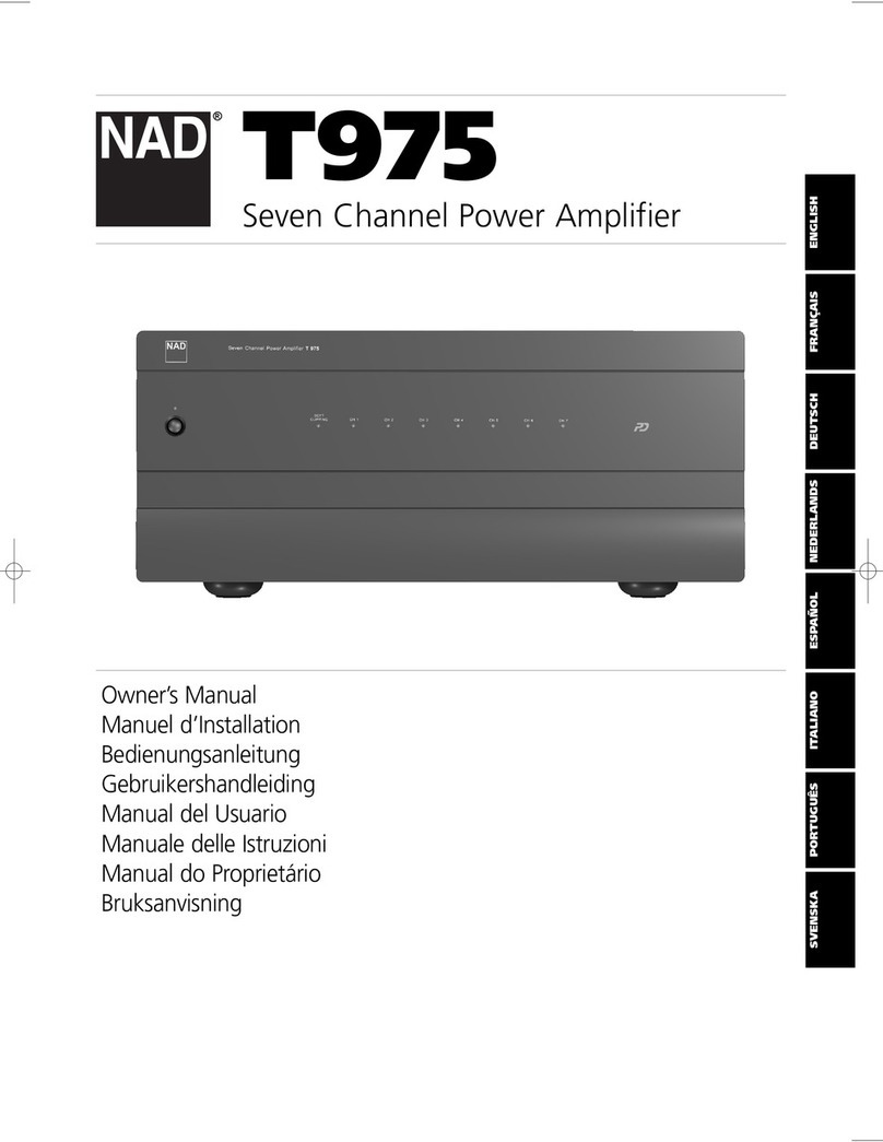
Ecler PAM4100 User manual

SERVICE MANUAL
SIGNAL
PROTECT
THERMALTHERMAL
BRIDGED
PROTECT
6
100
1
2
4
3
5
9
8
SIGNAL
CLIP
7
1
2
0
3
45
9
10
8CLIP
6
7
ON
OFF
SWITCHING POWER MOSFET AMPLIFIER
CHANNEL I CHANNEL II
THERMAL
PROTECT
SIGNAL
PROTECT
BRIDGED
10
0
1
2
9
8
SIGNAL
CLIP
1
2
010
9
8CLIP
THERMAL
6
4
3
5
7 3
5
46
7
ON
OFF
SWITCHING POWER MOSFET AMPLIFIER
CHANNEL I CHANNEL II

SERVICE MANUAL PAM6100 / 4100
INDEX
PAM6100
-BLOCK DIAGRAM
-FUNCTIONING DESCRIPTION
SCHEMATICS
Inputs circuit
Power Amplifier circuit
Soft-Start Power Supply circuit
Potentiometers and leds circuit
Capacitors circuit
Speak on circuit
-COMPONENTS LOCATION SCHEMA
AND PARTS LIST
Inputs circuit
Power Amplifier circuit
Soft-Start Power Supply circuit
Potentiometers and leds circuit
Capacitors circuit
Speak on circuit
-TESTING AND QUALITY CONTROL
-TECHNICAL CHARACTERISTICS
-WIRING DIAGRAM
-MECHANICAL DIAGRAM
-PACKING DIAGRAM
PAM4100
-COMPONENTS LOCATION SCHEMA
AND PARTS LIST
Power Amplifier circuit
-MECHANICAL DIAGRAM

SHUTDOWN
SHUTDOWN
INPUT CIRCUIT
S.P.
OFF
CH 2
S.P.
20Hz
HIGH PASS FILTER
OFF
40Hz
30Hz 20Hz
30Hz
40Hz
VCA
-Vref
VOLUME
AC DETECT
BRIG
MODULES
OPTIONAL
BRIG
PROTECT
OUTPUT
CONTROL
ANTICLIP
AND TIMER
PROTECTION RELAY
OUTPUT
CLIP
HIGH PASS FILTER
CH 1
THERMAL PROCESSOR
THERMAL PROCESSOR
THERMAL PROTECT
FAN CONTROL
THERMAL
OPTIONAL
STEREO
MODULES
PROBE
TRANSFORMER
PROBE
MODULE
THERMAL
-Vref
VCA
THERMAL
ADJ 0dB
CONTROL
VOLUME
FAN
CROWBAR
POWER MODUL CIRCUIT
OUT 2
POWER MODUL CIRCUIT
LEVEL
CONVERTER
DRIVER MOSFET N
OVERLOAD
LOW SIDE
-Vcc
LEVEL
CONVERTER
FEEDBACK
DRIVER MOSFET N
MIRROR
WILSON
CURRENT
ZOBEL
DC PROTECT
HIGH SIDE
OVERLOAD
OUT 1
++Vcc
+Vcc
+15V

author: Queralt date: 010418 project:
EP04-99
product:
PAM4/6100
approved:
num: 52.0010 version: 01.00
title:
FUNCTIONING DESCRIPTION
ECLER
EPO4-99 Power Module. Functioning description.
Due to the high power level required on the output load, the amplifier final stage's
structure differs from the design used untill now. This is due to the breakdown voltage
limit on P-channel MosFET's, wich is 200V. This final stage is formed by several
shunted MosFET's, where those of the positive branch are common-drain configured,
and the negative branch are mounted in common-source configuration.
The system's controlling device is a NE5534-type operational amplifier, wich is
internally compensated in order to obtain gain levels equal or higher than three. The
amplifier's feedback is given by a resistor and a capacitor associated to the operational
amplifier's non inverting input.
Transistors BF587 and BF588 are common-base configured, forming a current supply
structure. This specific transistor type is used because of the higher Vce voltage level
required by this design. They perform simultaneously two functions: they polarize the
MosFET's gate-source junctions, keeping them on the conducting edge, and they
tranfer the OpAmp's output voltage variations referred to signal ground.
The signal variations normally reflected by Q107 and referred to the positive power
supply, are now needed to be floating variations, and referred to the outputs. This
function is done by Q109-110 (BF588), wich are mounted formig a Wilson-type mirror
current supply. This mirror current supply transfers all of the current variations detected
while descending through Q109's collector, to similar variations on Q110's collector
also downward current. Resistors R167 and R174 are used to balance the current
mirror, in order to avoid the use of transistors with forcibly the same beta value. C138
and C141 suppress their resistance when high frequency signal is processed. Diodes
D126 and D127 avoid the transistors to get saturated, and R171 eliminates the loads
on BF588's bases (Baker Circuit).
The system requires about 12Vdc additional voltage upon the usual Vcc level, this
allows a correct saturation and a symetric clipping at the higher MosFET's.
The correct polarization current value is adjusted by a 4K7 potentiometer connected to
the BF transistor's emitter. This adds an additional current to the current source output
on th BF transistor's loading resistors.
In order to maintain the appropiate stand-by current level against varying temperature
conditions, BD437-type transistors are used. As they have a particular temperature-
depending base-emitter voltage curve, this voltage is used to keep a correct voltage
reference for the current supply. As the temperature rises, the reference voltage level
decreases, the gate-source voltage also decreases and, finally, the bias current also
decreases.
52-0010-0100 EP04-99 Anglès.xls 1 of 3

Transistors Q111 and Q112, and their corresponding twins at the lower branch, form
acurrent-buffering circuit wich allows afast charge and discharge of the power
MosFET's gates.
The Zobel circuit, aresistance-capacitance-inductance formed network associated to
the amplifier's ouput, tries to keep the amplifier's output load impedance constant no
matter wich load value is conected to the output, or wich frequency is processed, in
order to avoid phase shifts on the feedback signal.
To avoid the presence of DC voltage on the output, adiac-triac based system is used,
wich shorts the output to signal ground in case the DC level reaches the diac's
triggering value. To avoid this to happen when processing correct signal (sine
waveform, music...), the diac obtains its reference level from afiltering network formed
by a 100K resistor and a 1mF capacitor.
The protections circuitry overhauls the MosFET's power consumption. Basically, this
circuitry consists of two important sections: MosFET's Id current monitoring, and
MosFET's Vds value detection.
When the MosFET's Id level rises above acertain level, transistor Q119 (controlling
transistor) conducts and decreases the BF transistor's loading resistance, thus reducing
also their gate-source voltage and, finally, lowering the Id current value. This system is
helped by adelayed performance, due to the associated circuitry to Q145 and C174.
This capacitor starts to charge when acurrent level above the allowed value is
detected, and the protection starts. The greater is the capacitor's charge level, the
higher is also the voltage applied to Q119 controlling transistor's base, increasing its
conduction and, consequently, reducing the gate-source voltage and thus the Id current
value. This system uses afeedback network. The delay used is necessary to avoid
clipping the processed signal's dynamic range, wich should result in the typical clipping
noise. In the negative branch, the protection circuitry is associated to control transistor
Q120.
In case the overcurrent is not ocassional, and persists, after aperiod of time between
4and 10 seconds (determined by R142 and C124), the system switches back to
Stand-
by mode, due to asystem-reset. This is done by an optocoupler (IC113) associated to
the negative branch protection circuitry. When protections get activated, IC113
gradually charges C124 untill a40106-type Schmidt trigger gate switches over .If the
problem persists, this cycle is repeated.
STANDBY CIRCUITRY.
This circuit maintains the Output shutdown relay closed for about 10 seconds, and
thus annulates any current through the MosFET's during this period, just untill the
whole system's power supply voltage reaches its stable level. By this system, we avoid
to hear through the loudspeakers any possible annoying noise proceeding from the
system's start-up.
52-0010-0100 EP04-99 Anglès.xls 2 of 3

This delay time is achieved by using aRC cell, where R135=287K and
C119=47mF/50V. As this cell charges, its voltage increases untill reaching the
40106-
type Schmidt trigger (IC108) switching value; at this point, the relay opens and the
amplifier starts to function normally.
The discharge or reset of capacitor C119=47mF can be done by cutting off the power
supply, or by triggering the Thermal or other protections. During ashort period of time,
BC817-type transistor Q102 acts like aswitch, shunting two 750 ohm resistors to
C119.
Moreover, the amplifier includes some other additional features, like:
· Volume control by a VCA system.
· An ANTICLIP system.
· A Temperature control system.
The ANTICLIP system. When the amplifier reaches clipping levels, the operational
amplifier looses control on the system's performance and at its output some ±Vcc
voltage peaking pulses may appear, proceeding from its power supply. This peaking
pulses are used to be rectified and sent to an optocoupler (IC111), wich varies the
system's VCA control voltage as afunction of those pulse's amplitude, creating a
negative feedback wich should pull back the system into stable functioning area.
The Temperature control system has three main functions:
·Controlling the cooling fan speed, as it is afunction of the measured temperature. The
fan's operation voltage range is »7 to 4 Volt.
· Suspending the amplifier's functioning when the temperature exceeds »92ºC
·Reducing the amount of power output, depending on the module's temperature (as it
rises above 85ºC) and on the main power supply's transformer (above 120ºC).
The temperature control system consists on two LM35D-type IC's, wich act like a
thermal probe; one is placed on the amplifier's heat sink, and the other is placed into
the main power supply transformer's core. Moreover, three amplifiers, acomparator
for the thermal probe and a 7805-type IC to feed the cooling fan are used.
The first amplifier (1/4 IC114) acts on the cooling fan speed control. The second
amplifier (1/4 IC114) modifies the VCA gain control, in order to reduce the system's
gain if the temperature rises above 85ºC. The third amplifier (1/4 IC114) modifies the
VCA gain control, in order to reduce the system's gain if the temperature rises above
120ºC. The comparator (1/4 IC114) is responsible for the output shutdown relay
performance, in order to close it as the temperature reaches 92ºC, and thus cutting of
the amplifier's MosFETs bias current. As this happens, the signal output of the whole
unit is cutted off.
52-0010-0100 EP04-99 Anglès.xls 3 of 3


This manual suits for next models
1
Table of contents
Other Ecler Amplifier manuals

Ecler
Ecler NPA2500T User manual

Ecler
Ecler eGPA2-150 User manual

Ecler
Ecler SAM612T User manual

Ecler
Ecler HSA2-400ES User manual

Ecler
Ecler MPA4-80R User manual
Ecler
Ecler NZA4-70 User manual
Ecler
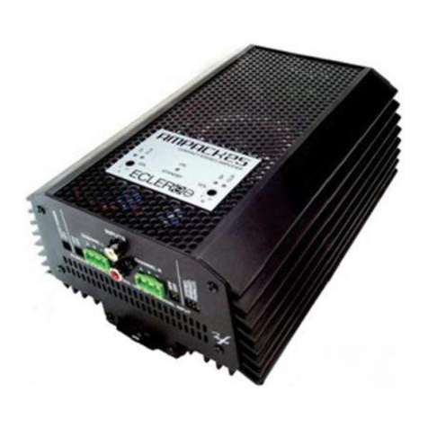
Ecler AMPACK Series User manual
Ecler
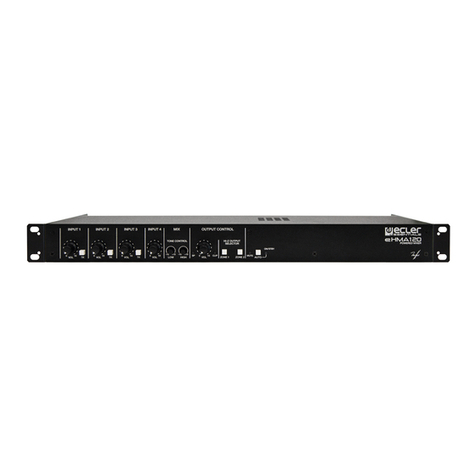
Ecler eHMA SERIES User manual

Ecler
Ecler DPA2500T User manual

Ecler
Ecler DT4800 User manual

