ECS P6SEP-Me User manual

Important Information
Copyright
This publication, including all photographs, illustrations and software, is protected
under international copyright laws, with all rights reserved. Neither this manual, nor
any of the material contained herein, may be reproduced without the express written
consent of the manufacturer.
Disclaimer
The information in this document is subject to change without notice. The
manufacturer makes no representations or warranties with respect to the contents
hereof and specifically disclaims any implied warranties of merchantability or fitness
for any particular purpose. Further, the manufacturer reserves the right to revise this
publication and to make changes from time to time in the content hereof without
obligation of the manufacturer to notify any person of such revision or changes.
Trademark Recognition
Microsoft, MS-DOS and Windows are registered trademarks of Microsoft Corp.
MMX, Pentium, Pentium-II, Celeron are a registered trademarks of Intel Corporation.
VGA, OS/2, PS/2 are registered trademarks of International Business Machines.
AMD, K5, K6 are registered trademarks of Advanced Micro Devices Inc.
Cyrix, M1 are registered trademarks of Cyrix Corporation.
Other product names used in this manual are the properties of their respective owners
and are acknowledged.
Version 3.0

Safety Compliance
Federal Communications Commission (FCC)
This equipment has been tested and found to comply with the limits for a Class B
digital device, pursuant to Part 15 of the FCC Rules. These limits are designed to
provide reasonable protection against harmful interference in a residential installation.
This equipment generates, uses, and can radiate radio frequency energy and, if not
installed and used in accordance with the instructions, may cause harmful interference
to radio communications. However there is no guarantee that interference will not
occur in a particular installation. If this equipment does cause harmful interference to
radio or television reception, which can be determined by turning the equipment off
and on, the user is encouraged to try to correct the interference by one or more of the
following measures:
♦Reorient or relocate the receiving antenna.
♦Increase the separation between the equipment and the receiver.
♦Connect the equipment onto an outlet on a circuit different from that to which
the receiver is connected.
♦Consult the dealer or an experienced radio/TV technician for help.
Shielded interconnect cables and shielded AC power cable must be employed with this
equipment to insure compliance with the pertinent RF emission limits governing this
device. Changes or modifications not expressly approved by the system’s
manufacturer could void the user’s authority to operate the equipment.
Declaration of Conformity
This device complies with part 15 of the FCC rules. Operation is subject to the
following conditions:
♦This device may not cause harmful interference, and
♦This device must accept any interference received, including interference that
may cause undesired operation.
Canadian Department of Communications
This class B digital apparatus meets all requirements of the Canadian Interference-
causing Equipment Regulations.
Cet appareil numérique de la classe B respecte toutes les exigences du Réglement sur
le matériel brouilieur du Canada.

43
Appendix 1: Quick Jumper Setting Reference
JP1: Clear CMOS memory jumper
Use this 3-pin jumper top clear all the current data stored in the CMOS memory.
Function Jumper Cap
Normal operation Short pins 1-2
Clear CMOS Short pins 2-3
JP2: Keyboard power on jumper
Use this 3-pin jumper to enable keyboard power on with hot keys or password.
Function Jumper Cap
Enable keyboard power on Short pins 2-3
Disable keyboard power on Short pins 1-2
JP6: Audio enable/disable jumper
Use this jumper to enable or disable the audio system integrated on the mainboard.
Function Jumper Cap
Enable audio Short Pins 1-2
Disable audio Short pins 2-3
JP3: Flash BIOS enable/disable jumper
Use this jumper to allow a new BIOS to be flashed to the mainboard BIOS chip.
Function Jumper Cap
Enable Flash BIOS Short Pins 1-2
Disable Flash BIOS Short pins 2-3
JP7: SPDIF output signal level jumper
Use this 2-pin jumper to set an SPDIF output signal of 0.5V or 5V
Function Jumper Cap
5 volts Short pins 1-2
0.5 volts Open pins 1-2
JP8: Modem enable/disable jumper
Use this 3-pin jumper to enable or disable the built-in fax/modem.
Function Jumper Cap
Enable onboard modem Short pins 1-2
Disable onboard modem Short pins 2-3
1 2 3
1 2 3
1 2 3
JP1
JP2
1 2
JP7
JP3
JP6
1
2
3
1 2 3
JP8

44
PANEL1: Panel connectors for switches and indicators
Use the panel connector to implement the switches and indicators on your system case.
Function Pins
Speaker 1, 3, 5, +7
Power Indicator +2, +4, 6
Keylock +8, 10
Green Indicator +13, 14
Hard Disk Indicator +15, 16
Reset Switch 17, 18
Suspend Switch 19, 20
Power Switch 21, 22
21
22 21
Speaker
Power LED
KeyLock
HDD LED
Reset SW
Suspend SW
Power SW
Green LED
PANEL1

T
Ta
ab
bl
le
e
o
of
f
C
Co
on
nt
te
en
nt
ts
s
Chapter 1: Introduction
Welcome.... ......... ......... ......... ........ ......... ......... .........1
About the Manual . ......... ......... ........ ......... ......... .........1
Checklist..... ......... ......... ......... ........ ......... ......... .........2
Features..... ......... ......... ......... ........ ......... ......... .........2
Chapter 2: Installation
Before You Begin . ......... ......... ........ ......... ......... .........5
Mainboard Guide.. ......... ......... ........ ......... ......... .........6
Preparing the Mainboard ......... ........ ......... ......... .........8
Install the Mainboard in the System Case .... ......... .........15
Chapter 3: Setup
About the Setup Utility .... ......... ........ ......... ......... .........19
Standard CMOS Setup Option.. ........ ......... ......... .........21
BIOS Feature Setup Option...... ........ ......... ......... .........22
Chipset Features Option. ......... ........ ......... ......... .........25
Power Management Setup Option ..... ......... ......... .........28
PNP/PCI Configuration Option.. ........ ......... ......... .........32
Load BIOS Defaults Option....... ........ ......... ......... .........33
Load Optimum Settings Option. ........ ......... ......... .........33
Integrated Peripherals Option ... ........ ......... ......... .........34
Password Settings ......... ......... ........ ......... ......... .........36
IDE HDD Auto Detection Option ........ ......... ......... .........36
Save and Exit Setup Option...... ........ ......... ......... .........37
Exit Without Saving Option ....... ........ ......... ......... .........37
Chapter 4: Software
About the Software......... ......... ........ ......... ......... .........38
Folder for this Mainboard ......... ........ ......... ......... .........38
Running the Support CD-ROM.. ........ ......... ......... .........40
Utility Folder Installation Notes.. ........ ......... ......... .........40
CMI8X38 Folder Installation Notes .... ......... ......... .........41
SiS_IDE Folder Installation Notes...... ......... ......... .........42
SiS620_VGA Folder Installation Notes......... ......... .........42
Mainboard Installation Notes..... ........ ......... ......... .........42
Appendix
1. Quick Jumper Setting Reference.... ......... ......... .........43


1
C
Ch
ha
ap
pt
te
er
r
1
1:
:
I
In
nt
tr
ro
od
du
uc
ct
ti
io
on
n
Welcome
Congratulations on your purchase of the P6SEP-Me mainboard. The P6SEP-Me
mainboard is a micro-ATX board measuring 243.8 mm by 200 mm and using a 4-layer
printed circuit board. This board features a PGA370 ZIF (Zero Insertion Force)
processor socket. This socket can be installed with the latest generation of Intel
Celeron processors that are packaged in a Plastic Pin Grid Array (PPGA), just like the
original Pentium processors. The mainboard supports a system bus speeds of 100 MHz
so you can use high-performance PC-100 memory. The mainboard has integrated
2D/3D graphics, and integrated 3D audio, so a usable system can be created with the
addition of just memory modules and a Celeron processor.
This chapter contains the following information:
lAbout the Manual explains how the information in this manual is
organized
lChecklist comprises a list of the standard and optional components that are
shipped with this mainboard,
lFeatures highlights the functions and components that make this one of
the best value mainboards on the market
About the Manual
The manual consists of the following chapters:
Introduction
Use the Introduction Chapter to learn about the features of the mainboard, and the
checklist of items that are shipped with the package.
Installation
Use the Installation Chapter to learn how to install the mainboard and get your system
up and running.
Setup
Use the Setup Chapter to configure the mainboard for optimum performance.

2
Software
Use the Software Chapter to learn how to use the software drivers and support
programs that are provided with this mainboard.
Checklist
Compare the contents of your mainboard package with the standard checklist below. If
any item is missing or appears damaged, please contact the vendor of your mainboard
package.
Standard Items
ü
1 x P6SEP-Me Mainboard
ü
1 x Cable/Bracket Pack
Diskette drive ribbon cable
IDE drive ribbon cable
ü
This User’s Manual
ü
Software Support CD-ROM Disc
Optional Items
1 x V 9.0 Fax/Modem Card
Features
This is a powerful platform that combines the low-cost/high-performance features of
the new generation of Celeron processors with a 100 MHz system bus so that you can
utilize high-performance PC-100 memory modules.
Low-cost/high-performance Processing
Intel’s new generation of Celeron processors are shipped in the familiar PPGA square
plastic package that are common to all Pentium and Pentium-compatible processors.
The mainboard has a PGA370 ZIF socket for the installation of the Celeron. (Note that
the socket has a different pinout than Pentium/Pentium compatibles and cannot be
used by Socket-7 processors.) The Celeron processor features Pentium-II performance
with internal clock speeds of 300, 333, 366, 400, 433, 466 and 500 MHz, 32K of level-
1 cache memory, and 128K of level-2 cache memory. This mainboard allows entry-
level and business-class users to move up to Pentium-II performance at minimum cost.
Configuration for different processor speeds is automatically set by firmware and
motherboard switch or jumper settings are not required.

3
High-performance Memory
The board has three DIMM sockets for the installation of 168-pin, 3.3V non-buffered
DIMM memory modules. The DIMM memory modules must be installed with
SDRAM memory chips. The board supports a memory bus of 100 MHz, so you must
install high-performance PC-100 memory modules. Each installed memory module
can be populated with 16 MB up to 512 MB of memory, so a total of 1.5 GB of
memory can be installed. The integrated video system uses a shared memory
architecture so that you must reserve some of the installed memory as video memory
using the system BIOS. You must install at least one memory module, and the first
memory module is installed in DIMM1.
Highly Integrated Design
This mainboard features a high level of integrated functions provided by the onboard
chipsets. The SiS 620 Pentium-II PCI/AGP/3D VGA chipset provides all the north
bridge support –Pentium-II CPU and memory addressing, integrated DRAM
controller, PCI-IDE controller, AGP 3D graphics sub-system, and PCI-bus interface.
The SiS 5595 provides the south bridge support –ACPI-compliant power management,
real-time clock, and USB interface. The Winbond W83877TF is a single chip I/O
solution, and the CMI8738 provides the onboard 3D audio feature. This highly
integrated mainboard ensures stability and allows a fully functional system to be
created by adding just a processor and memory.
Built-in AGP 3D-Graphics
This mainboard features a built-in 3D-graphics controller integrated in the SIS 620
chipset. The graphics controller uses a shared memory architecture that allows it use
either 2 MB, 4 MB, or 8 MB of the system’s main memory. The graphics controller
has hardware accelerators for both 3D and 2D graphics and an MPEG decoder for
DVD video playback. The graphics system will support extended high-resolution
displays up to 1600 x 1200. At an XGA resolution of 1024 x 768, the graphics system
supports a color depth of 16 million colors.
Built-in PCI 3D Sound
The CMI8738 is a single chip solution for PCI-bus 3D audio. The chip provides Sound
Blaster 16-bit-compatible audio, plus support for Microsoft’s DirectSound 3D
specification and Aureal A3D interface. The sound ports include jacks for speakers,
microphone and stereo in, and a game/MIDI port. The audio system supports full
duplex operation and drivers are available for WIN 95/98 and WIN NT 4.0. The audio
system can output sound to 4 loudspeakers and also supports SPDIF 24-bit digital
sound input and output.
Optional Built-in Communications
The mainboard has an integrated fax/modem connector. As an option, you can
purchase a fax/modem extension bracket which connects the line and telephone RJ11

4
socket s to the board. The fax/modem supports the V.90 protocol that allows
transmissions at up to 56Kbps and is fully compatible with earlier transmission and
error correction standards. It supports automatic fall back and caller ID.
Solid Expansion Options
Because this is a highly integrated board with built-in audio and a full set of I/O ports,
it does not require a full set of expansion slots. The board provides three usable slots.
The board has three 32-bit PCI slots and one 8/16-bit ISA slot. The ISA slot is shared
with one of the PCI slots meaning that you can use either the ISA slot or the PCI slot,
but not both at the same time.
Integrated I/O
Using the Winbond W83877TF I/O chip and the SiS 620 chipset, the board has a
comprehensive set of integrated I/O ports. The I/O port array features PS/2 keyboard
and mouse ports, a parallel port, two USB ports, one serial port, a monitor port, a
game/MIDI port, and three audio jacks. Optionally, you can use the built-in mainboard
headers to add in an infrared port or a second serial port. The mainboard has two PCI-
IDE channels and a floppy disk drive interface.
Keyboard Power On Feature
Using the system BIOS setup program, you can configure the system to turn on using
a keyboard-typed password. A green keyboard is not required.
Programmable Firmware
The mainboard includes Award BIOS which allows BIOS setting of CPU parameters.
The fully programmable firmware enhances the system features and allows users to set
power management, CPU and memory timing, LAN and modem wake-up alarms, and
so on. The firmware can also be used to set parameters for different Celeron processor
clock speeds so that you don’t need to change mainboard jumpers and switches.

5
C
Ch
ha
ap
pt
te
er
r
2
2:
:
I
In
ns
st
ta
al
ll
la
at
ti
io
on
n
Before You Begin
Before you begin to install your P6SEP-Me mainboard, take some precautions to ensure
that you avoid the possibility of damage to the product from static electricity.
Ensure too that you are installing the mainboard into a suitable case.
Static Electricity
In adverse conditions, static electricity can accumulate and discharge through the
integrated circuits and silicon chips on this product. These circuits and chips are
sensitive and can be permanently damaged by static discharge.
♦If possible wear a grounding wrist strap clipped to a safely grounded device
during the installation.
♦If you don’t have a wrist strap, discharge any static by touching the metal case of
a safely grounded device before beginning the installation.
♦Leave all components inside their static-proof bags until they are required for the
installation procedure.
♦Handle all circuit boards and electronic components carefully. Hold boards by
the edges only. Do not flex or stress circuit boards.
Choosing a Case
The P6SEP-Me mainboard complies with the specifications for a micro-ATX board. The
micro-ATX format features small size, fewer expansion slots and smaller power
consumption, so that the system case is less expensive. You can also install this kind of
board into a full-size ATX case.
Some features on the mainboard are implemented by cabling connectors on the
mainboard to indicators and switches on the system case. Ensure that your case supports
all the features required. The P6SEP-Me mainboard can support one or two floppy
diskette drives and four enhanced IDE drives. Ensure that your case has sufficient power
and space for all the drives that you intend to install.
The mainboard has a set of I/O ports on the rear edge. Ensure that your case has an I/O
template that supports the I/O ports and expansion slots.

6
Mainboard Guide
Use the following illustration and key to identify the components on your mainboard.
Key to Mainboard Components
Component Description
ISA1 1 x 8/16-bit ISA expansion slots
PCI 1,2,3 3 x 32-bit PCI expansion slots
SOCKET PGA 370 Processor socket for Celeron processor
DIMMs 1, 2, 3 Slots for 168-pin memory module
FDD1 Connector for floppy disk drives
IDE1, IDE2 Primary and secondary IDE channels
ATX1 Connector for ATX power supply
SIR1 Connector for optional infrared port
PANEL1 Panel connector for switches and indicators
FAN1 Power connector for CPU cooling fan
FAN2 Power connector for case cooling fan
WOM1 Connector for modem wake up
WOL1 Connector for LAN wake up
SPDIF SPDIF In/out connector (professional 24-bit digital audio
interface)
1
1
1
1
SOKET
PGA 370
DIMM2
DIMM1
DIMM3
ATX1
FDD1
IDE2
IDE1
FAN2
FAN1
JP1
JP6
J3
JP7
PCI1
PCI2
PCI3
ISA1
JP3
SIR1
COM2
PANEL1
WOM1
WOL1
J2
JP2
JP8

7
COM2 Connector for optional second serial port
J2 Auxiliary audio connector for optional CD-ROM drive
J3 Audio connector for optional CD-ROM drive
JP1 Clear CMOS memory jumper
JP2 Keyboard power on jumper
JP3 Flash BIOS enable/disable jumper
JP6 Audio enable/disable jumper
JP7 Connector for fax/modem adapter card
JP8 Enable/disable onboard modem jumper
Side View of the Input/Output Ports
PS2KBM1
USB1
COM1
VGA1
JS1
LPT1
JS1
Key to I/O Ports
Component Description
PS/2 port for pointing device (upper port)PS2KBM1 PS/2 port for keyboard (lower port)
LPT1 External parallel port
JS1 (Upper) External game/MIDI port
JS1 (Lower) Audio jacks for (from left to right) line out, line in, microphone
VGA1 External monitor port
COM1 External serial port 1/3
USB1 Two stacked Universal Serial Bus ports
8
Preparing the Mainboard
Prepare the main board by installing the Celeron Pentium-II processor and then
installing either 1, 2 or 3 memory modules. This board supports the new generation
Celeron processor that is packaged in a Plastic Pin Grid Array (PPGA) designed to fit
the PGA370 ZIF socket on the mainboard. You can use a Celeron that runs at either 300,
333, 366, 400 or 500 MHz. Next, install one or more memory modules. Finally, review
all the important jumper settings to ensure that the board is configured correctly.
Install the Processor
This mainboard is installed with a PGA370 ZIF processor socket. This socket will only
support the PPGA Celeron processor. Do not try to insert a socket-7 processor such as a
Pentium or Pentium-compatible processor. The Celeron processors all run over a 66
MHz system bus and have internal clock speeds ranging from 300 to 433 MHz.
Configuration of the processor is made automatically using the mainboard BIOS (see the
Setup chapter).
Follow the steps below to install the Celeron processor in the PGA370 socket.
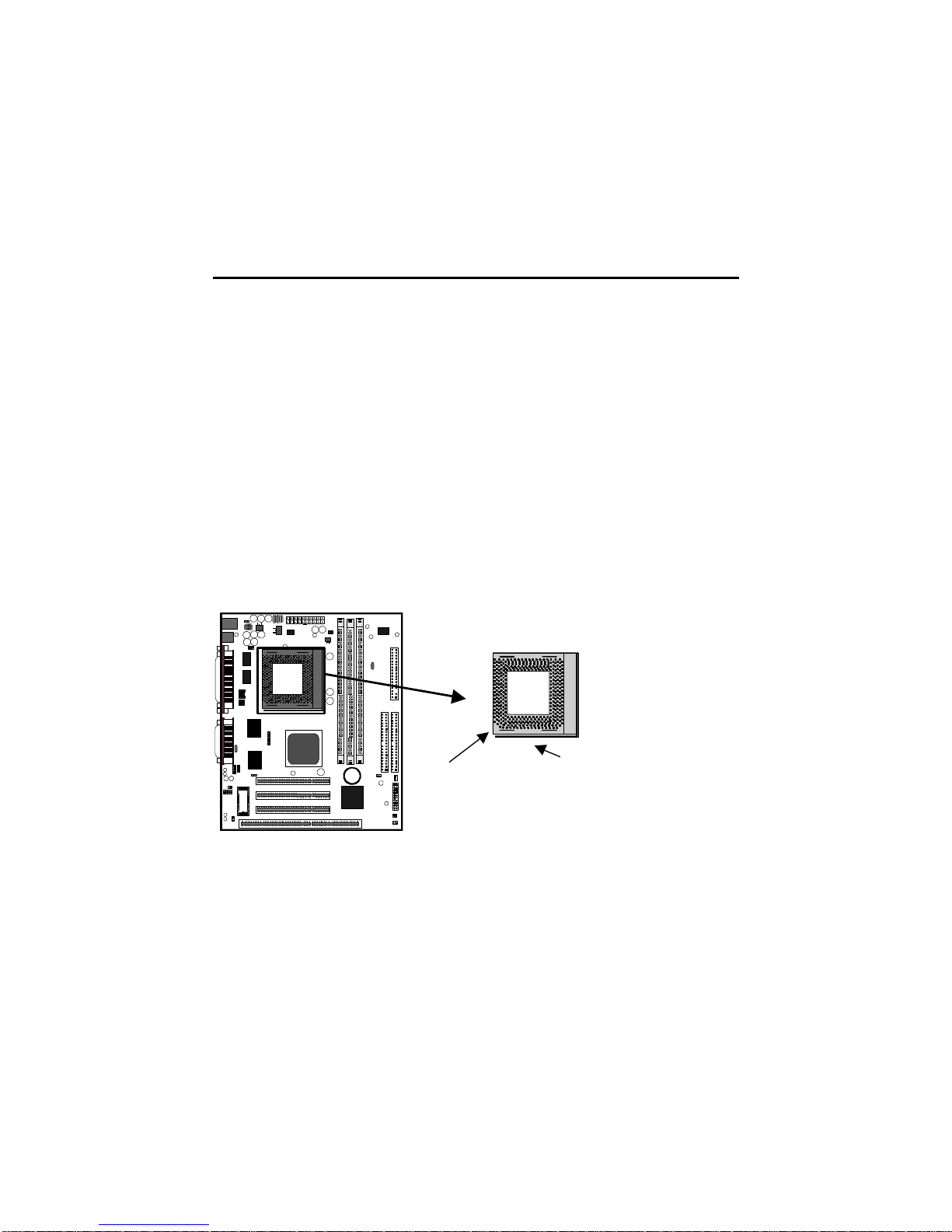
1. Locate the zero insertion force (ZIF) PGA370 socket for the processor.
1
1
1
1
2. On the socket and on the processor, identify the pin 1 corner. You can identify the
pin 1 corner by noting that in the rectangular matrix of holes on the socket, one hole
is absent on two corners. The front corner with the absent hole is the pin-1 corner.
On the processor, the pin-1 corner is beveled (see the illustration below).
3. Push the socket locking lever away from the socket to unhook it. Swing the lever
into the upright position.
4. Insert the processor into the socket taking care that you have matched the pin 1
corners. No force is required, and the processor should seat smoothly into the
socket.
Pin-1 corner
Typical Socket-PGA370
Locking Lever
9
5. Swing the locking lever down and hook it under the latch on the side of the socket
to lock it in place.
6. Locate the power connector for the processor cooling fan FAN1. If your processer
has a cooling fan installed, connect the cable from the cooling fan to FAN1.
1
1
1
1
FAN1
Socket
PGA370
Processor
Locking Lever
Pin-1 Corner
Pin-1 Corner
3 2 1

10
Install the Memory Modules
For this mainboard, you must use 168-pin 3.3V non-buffered Dual In-line Memory
Modules (DIMMs). The memory chips must be SDRAM (Synchronous Dynamic
Random Access Memory). The memory bus can run from 66 MHz through to 100 MHz
so you can either use inexpensive 66 MHz memory, or higher performance PC-100
memory. You can use memory modules that have a capacity of 16 MB up to 512 MB.
Total installed memory can be up to 1.5 GB.
You must install at least one memory module and the first memory module should be
installed in slot DIMM1, the second in slot DIMM2 and the third in slot DIMM3. You
can use memory modules which have memory chips on just one side (single-sided) or
memory chips on both sides (double-sided).
1. Locate the DIMM slots on the mainboard.
2. The DIMM slots are keyed with notches and the DIMMs are keyed with cut-outs so
that they can only be installed correctly. Check that the cut-outs on the DIMM
module edge connector match the notches in the DIMM slot.
3. Push the latches on each side of the DIMM slot down.
4. Install the DIMM module into the slot and press it carefully but firmly down so that
it seats correctly. The latches at either side of the slot will be levered upwards and
latch on to the edges of the DIMM when it is installed correctly.
DIMM (Dual In-line Memory Module)
DIMM Slot
Latch
Latch
1
1
1
1
DIMM Slots

11
Check all the Jumper Settings
Check all the mainboard jumpers to ensure that the board is configured correctly.
A Note on Jumpers
A jumper consists of two or more pins mounted on the mainboard. Some jumpers
might be arranged in a series with each pair of pins numbered differently.
Jumpers are used to change the electronic circuits on the mainboard. When a
jumper cap is placed on two jumper pins, the pins are SHORT. If the jumper
cap is removed (or placed on just a single pin) the pins are OPEN.
JP1: Clear CMOS Memory Jumper
This jumper lets you erase the system setup settings that are stored in CMOS memory.
You might need to erase this data if incorrect settings are preventing your system from
operating. To clear the CMOS memory, turn off the system, disconnect the power cable
from the mainboard, and short the appropriate pins for a few seconds.
Function Jumper Cap
Normal operation Short pins 1-2
Clear CMOS Short pins 2-3
1
1
1
1
1 2 3
JP1

12
JP2: Keyboard Power On Jumper
This jumper lets you use a typed-in password as a power switch to turn your system on.
If you enable this property, you need to define the password or the hot keys using the
setup utility. See Chapter 3 for more information.
Function Jumper Cap
Enable keyboard
power on Short pins 2-3
Disable keyboard
power on Short pins 1-2
JP6: Audio System Enable/disable Jumper
This jumper lets you enable or disable the audio system that is integrated on the
mainboard. You must disable the audio system if you install an alternative sound card
using one of the expansion slots.
Function Jumper Cap
Enable audio Short Pins 1-2
Disable audio Short pins 2-3
1
1
1
1
JP2
JP6
1 2 3
1 2 3

13
JP3: Flash BIOS Enable/Disable Jumper
The BIOS on this mainboard is stored on an Erasable Programmable Read Only Memory
(EPROM) chip. This means that you can erase the current BIOS and install an updated
BIOS whenever new upgrades are released. See Chapter 4 for information on using the
Flash BIOS utility. Before erasing the old BIOS and flashing a new BIOS, you must set
JP3 to Enable. After the new BIOS is installed, set JP3 to Disable so that the BIOS
cannot be erased by accident.
Function Jumper Cap
Enable Flash BIOS Short Pins 1-2
Disable Flash BIOS Short pins 2-3
JP7: Fax/modem Extension Bracket
The fax/modem extension bracket is supplied with this mainboard.
1. Locate the JP7 fax/modem connector on the mainboard.
2. Remove the expansion slot blanking plate from the system chassis that is adjacent to
the fax/modem connector.
3. Install the fax/modem extension bracket on to the MDM1 connector as shown below.
The RJ11 Line and Telephone sockets on the bracket are positioned in the expansion
slot with the removed blanking plate.
1 2 3
1
1
1
1
JP3
Line and Tel
RJ11 sockets Fax/modem
extension bracket
JP7
fax/modem
connector

14
JP8: Modem enable/disable jumper
Use this 3-pin jumper to enable or disable the built-in fax/modem.
Function Jumper Cap
Enable onboard modem Short pins 1-2
Disable onboard modem Short pins 2-3
1 2 3
JP8
1
1
1
1
Table of contents
Other ECS Motherboard manuals


 user manual")


