EG&G ORTEC 426 Service manual

mi
n
Model
426
Linear
Gate
Operating
and
Service
Manual
Model
426
Linear
Gate
Operating
and
Service
Manual
This
manual
applies
to
instruments
marked
"Rev
23"
on
rear
panel
Printed
in
U.S.A.
EG&G
ORTEC
Part
Number
733200
2740
1
.OC
0787

standard
Warranty
for
EG&G
ORTEC
Nuclear
Electronic
Instruments
EG&G
ORTEC
warrants
that
the
items
will
be
delivered
free
from
defects
in
material
or
workmanship.
EG&G
ORTEC
makes
no
other
warranties,
express
or
implied,
and
specifically
NO
WARRANTY
OF
MERCHANTABILITY
OR
FITNESS
FOR
A
PARTICULAR
PURPOSE.
EG&G
ORTEC's
exclusive
liability
is
limited
to
repairing
or
replacing
at
EG&G
ORTEC's
option,
items
found
by
EG&G
ORTEC
to
be
defective
in
workmanship
or
materials
within
two
yearsfrom
the
date
of
delivery.
EG&G
ORTEC's
liability
on
any
claim
of
any
kind,
including
negligence,
loss
or
damages
arising
out
of,
connected
with,
or
from
the
performance
or
breach
thereof,
or
from
the
manufacture,
sale,
delivery,
resale,
repair,
oruseof
any
item
or
services
covered
by
this
agree
ment
or
purchase
order,
shall
in
no
case
exceed
the
price
allocable
to
the
item
or
service
furnished
or
any
part
thereof
that
gives
rise
to
the
claim.
In
the
event
EG&G
ORTEC
fails
to
manufacture
or
deliver
items
called
for
in
this
agreement
or
pur
chase
order,
EG&G
ORTEC's
exclusive
liability
and
buyer's
exclusive
remedy
shall
be
release
of
the
buyer
from
the
obliga
tion
to
pay
the
purchase
price.
In
no
event
shall
EG&G
ORTEC
be
liable
for
special
or
consequential
damages.
Quality
Control
Before
being
approved
for
shipment,
each
EG&G
ORTEC
nuclear
electronic
instrument
must
pass
a
stringent
set
of
quality
control
tests
designed
to
expose
any
flaws
in
materials
or
workmanship.
Permanent
records
of
these
tests
are
maintained
for
use
in
warrany
repair
and
as
a
source
of
statistical
information
for
design
improvements.
Repair
Service
If
it
becomes
necessary
to
return
this
instrument
for
repair,
it
is
essential
that
Customer
Services
be
contacted
in
advance
of
its
return
so
that
a
Return
AuthorizSlfon
Number
can
be
assigned
to
the
unit.
Also,
EG&G
ORTEC
must
be
informed,
either
in
writing,
by
telephone
((615)
482-4411
]
or
by
telex
(55-7450)
of
the
nature
of
the
fault
of
the
instrument
being
re
turned
and
of
the
model,
serial,
and
revision
("Rev"
on
rear
panel)
numbers.
Failure
to
do
so
may
cause
unnecessary
delays
in
getting
the
unit
repaired.
The
EG&G
ORTEC
standard
procedure
requires
that
instruments
returned
for
repair
pass
the
same
quality
control
tests
that
are
used
for
new-production
instruments.
Instruments
that
are
returned
should
be
packed
so
that
they
will
withstand
normal
transit
handling
and
must
be
shipped
PREPAID
via
Air
Parcel
Post
or
United
Parcel
Service
to
the
nearest
EG&G
ORTEC
repair
center.
(In
the
case
where
the
instrument
did
not
function
upon
pur
chase,
EG&G
ORTEC
will
pay
shipment
costs
both
ways.)
The
address
label
and
the
package
should
include
the
Return
Authorization
Number
assigned.
Instruments
being
returned
that
are
damaged
in
transit
due
to
inadequate
packing
will
be
repaired
at
the
sender's
expense,
and
it
will
be
the
sender's
responsibility
to
make
claim
with
the
shipper.
Instruments
not
in
warranty
will
be
repaired
at
the
standard
charge
unless
they
have
been
grossly
misused
or
mishandled,
in
which
case
the
user
will
be
notified
prior
to
the
repair
being
done.
A
quotation
will
be
sent
with
the
notification.
Damage
in
Transit
Shipments
should
be
examined
immediately
upon
receipt
for
evidence
of
external
or
concealed
damage.
The
carrier
making
delivery
should
be
notified
immediately
of
any
such
damage,
since
the
carrier
is
normally
liable
for
damage
in
shipment.
Packing
materials,
waybills,
and
other
such
documentation
should
be
preserved
in
order
to
establish
claims.
After
such
notification
to
the
carrier,
please
notify
EG&G
ORTEC
of
the
circumstances
so
that
assistance
can
be
provided
in
making
damage
claims
and
in
providing
replacement
equipment
if
necessary.

Ill
CONTENTS
Page
WARRANTY
'i
PHOTOGRAPHS
iv
1.
DESCRIPTION
1
2.
SPECIFICATIONS
1
2.1
Performance
1
2.2
Controls
1
2.3
Inputs
1
2.4
Output
2
2.5
Electrical
and
Mechanical
2
2.6
Related
Equipment
2
3.
INSTALLATION
2
3.1
Connection
to
Power
2
3.2
Input
Signal
Connection
to
Linear
Gate
2
3.3
Logic
Input
to
the
Enable
Input
2
3.4
Logic
Inputs
to
the
DC
Inhibit
Input
3
3.5
Linear
Output
Signal
Connections
and
Terminating
Impedance
Considerations
3
4.
OPERATIONS
3
4.1
Front
Panel
Controls
3
4.2
Initial
Testing
and
Observation
of
Pulse
Waveforms
4
4.3
Connector
Data
4
4.4
Typical
Operating
Considerations
4
5.
CIRCUIT
DESCRIPTION
5
5.1
Linear
Gate
—
Etched
Board
426-0201
5
6.
MAINTENANCE
6
6.1
Testing
the
Performance
of
the
Linear
Gate
6
6.2
Adjustment
of
Linear
Gating
Duration
6.3
Adjustment
of
Linear
Gate
Pedestal
6.4
Tabulated
Test
Point
Voltages
6.5
Suggestions
for
Troubleshooting
6.6
Factory
Repair
Block
Diagram
and
Schematic
426-0200-B2
426-0000-S2
ILLUSTRATIONS
4
Fig.
4.2
Output
of
Linear
Gate
^
Fig.
4.1
Gating
Action
of
Linear
Gate.
IV
-
'■?'
'^'■1
""r---
-.
V
g^-M
i
"
-r
%,
.
iiSsiss#
O
426
O
UNEAR
GATE
GATE
WIDTH
'H'f:,;
.
^
,»»^e
--
<v,-^
W9iBxMSIs§MliSSM
'
'
'■
-
•
1
s«®Slafai
:->El^;
DC
INHIIilT
INPUT
.'»
^
'
-
'..
.
-1
-
'
'J..
•
■
■;
"-U^"
'
Ut
sJ^sSsftpfsPiH
iili^M
'•.
'
i
111
j
lii
'■
^5
r:W;^-3
/■:
j
'
i
:'
.

ORTEC
426
LINEAR
GATE
1.
DESCRIPTION
The
ORTEC
426
is
a
modular
Linear
Gate
that
provides
a
variable
gate
duration
whose
width
is
control
led
by
a
single-
turn
front-panel-mounted
potentiometer.
The
nominal
gate
duration
range
is
from
0.3
to
4
fisec.
Operation
of
the
Linear
Gate
is
controlled
by
the
application
of
a
positive
Enable
pulse.
The
Linear
Gate
is
useful
in
appl
ications
that
require
inhibiting
a
linear
signal
according
to
chosen
coincidence
or
timing
requirements,
e.g.,
reducing
the
counting
rate
in
sub
sequent
l
inear
analysis
equipment.
The
426
is
designed
to
meet
the
recommended
interchange-
abil
ity
standards
of
USAEC
Report
TID-20893
(Rev.)
.
An
ORTEC
401/402
Series
Bin
and
Power
Supply
provides
all
necessary
power
through
the
rear
module
power
connector.
All
signal
levels
and
impedances
are
compatible
with
other
modules
in
the
ORTEC
400
Series.
The
basic
function
of
the
426
is
to
accept
al
l
pulse
shapes
existing
in
the
ORTEC
400
Series
l
inear
function
modules.
If
the
input
signal
is
bipolar,
the
negative
portion
wi
l l
not
be
passed
through
the
Linear
Gate.
The
input
impedance
is
greater
than
5000^2,
and
the
input
is
normal
ly
sent
from
the
factory
ac-coupled.
The
input
can
be
operated
dc-coupled
if
desired
(refer
to
Section
4.4).
A
dc-restoration
network
at
the
input
reduces
basel
ine
shift
at
high
counting
rates.
The
restoration
network
works
on
both
unipolar
and
bipolar
in
put
pulse
shapes.
The
Linear
Gate
proper
consists
of
a
series-
paral
lel
saturated
transistor
switch.
This
switch
network
incorporates
an
adjustment
that
allows
the
Linear
Gate
to
operate
with
no
pedestal.
The
series-parallel
transistor
switch
is
activated
by
a
transistor-pair
current
switch.
This
latter
switch
is
activated
by
,the
gate
control
pulse
which
is
generated
with
the
appl
ication
of
an
externally
generated
Enable
pulse.
The
output
of
the
Linear
Gate
circuit
is
fed
into
a
cascode
emitter-fol
lower
cable
driver.
The
ORTEC
426
has
two
operating
modes:
normally
blocks
all
input
signals
not
accompanied
by
an
Enable
pulse
and
normal
ly
passes
all
signals
unless
accompanied
by
an
Inhibit
signal.
The
Inhibit
signal
can
be
fed
into
the
front
panel
Enable
connector
for
Pulse
Inhibit
operation
or
into
the
DC
Inhibit
Input
connector
for
dc
or
continuous
inhibit
opera
tion.
2.
SPECIFICATIONS
2.1.
PERFORMANCE
Gain
Unity.
Integral
Nonlinearity
<0.15%
from
0.2
to
10
V.
Pulse
Feedthrough
<10
mV
with
a
lO-V
input
pulse.
Temperature
Stability
<0.015%/°C,
0
to
50°C.
Counting
Rate
The
gain
shift
of
a
4-V
reference
pulse
is
<0.25%
with
the
application
of
an
additional
count
rate
of
65,000
counts/sec
of
6.0-V
random
pulses.
furnished
through
the
Enable
input
connector,
which
is
on
the
front
panel,
or
the
DC
Inhibit
Input
connector
on
the
rear
panel:
Norm
Input
pulse
wi
ll
be
gated
through
to
the
output
during
a
gate
width
interval
fol
lowing
the
leading
edge
of
each
Enable
input
pulse.
Pulse
Inhibit
Input
pulses
wil
l
be
inhibited
from
passing
through
the
output
during
a
gate
width
interval
following
each
Bnable
input
pulse.
DC
Inhibit
Input
pulses
wi
l l
be
inhibited
from
passing
through
the
output
during
intervals
of
pulses
or
dc
levels
through
the
DC
Inhibit
Input
connector
on
the
rear
panel.
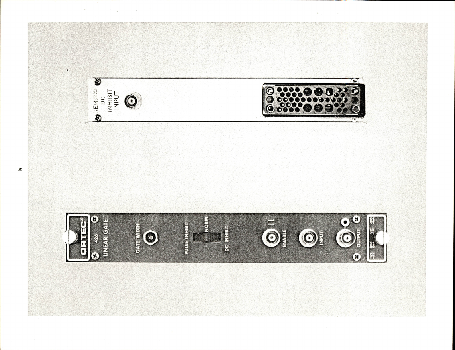
2.2.
CONTROLS
Gate
Width
Continuously
variable
from
0.3
to
4
fjsec.
Output
Pedestal
Adjustable
to
<1
mV.
Pulse
Inhibit/Norm/DC
Inhibit
3-position
mode
switch
that
permits
selection
of
the
function
of
any
pulse
or
dc
level
2.3.
INPUTS
Input
Unipolar
or
bipolar
with
positive
portion
leading.
Rated
range
0.2
to
10
V,
12
V
maximum.
Input
impedance
>5000T2.
BNC
connector
on
front
panel
.
Enable
(or
Inhibit)
Any
positive
input
>2
V,
maximum
in
put
20
V.
Enable
impedance
1000^2,
dc-coupled;
Inhibit
impedance
65012,
dc-coupled.
Front
panel
BNC
connector
for
each.
DC
Inhibit
Rear
panel
BNC
connector;
inhibits
input
pulses
from
passing
through
the
output
during
intervals
of
pulses
or
dc
levels;
impedance
65012,
dc-coupled.
Weight
(Shipping)
4.0
lb
(1.82
kg).
Weight
(Net)
2.1
lb
(0.96
kg).
Dimensions
Single-width
module
(1.35
by
8.714
in.)
per
TID-20893
(Rev.).
2.4.
OUTPUT
Rated
output
range
0.2
to
10
V
positive;
12
V
maximum.
Output
impedance
~212,
short-circuit
protected.
BNC
con
nector.
2.5.
ELECTRICAL
AND
MECHANICAL
Power
Requirements
-1-24
V,
30
mA;
-H2
V,
16
mA;
.
-24
V,
49
mA;
-12
V,
4.9
mA.
2.6.
RELATED
EQUIPMENT
The
input
to
the
linear
gate
of
the
426
can
be
from
any
of
the
linear
circuitry
in
theORTEC
NIM-standard
modules.
In
typical
applications
the
output
of
the
linear
gate
feeds
a
multichannel
analyzer
directly.
The
output
is
also
compatible
with
any
of
the
linear
modular
circuitry
in
the
ORTEC
NIM-
standard
modules.
3.
INSTALLATION
The
ORTEC
426
contains
no
internal
power,
but
is
used
in
conjunction
with
an
ORTEC
401
/402
Series
Bin
and
Power
Supply,
which
is
intended
for
rack
mounting.
Therefore
if
vacuum
tube
equipment
is
operated
in
the
same
rack
with
the
426,
there
must
be
sufficient
cooling
air
circulating
to
prevent
any
localized
heating
of
the
all-transistor
circuitry
used
throughout
the
426.
The
temperature
of
equipment
mounted
in
racks
can
easily
exceed
120°F
(50°C)
unless
precautions
are
taken.
The
426
should
not
be
subjected
to
temperatures
in
excess
of
120°F
(50
C).
3.1.
CONNECTION
TO
POWER
Turn
off
the
Bin
power
supply
when
inserting
or
removing
modules.
The
ORTEC
400
Series
is
designed
so
that
it
is
not
possible
to
overload
the
Bin
power
supply
with
a
full
complement
of
modules
in
the
Bin.
Since,
however,
this
may
not
be
the
case
when
the
Bin
contains
modules
of
other
than
ORTEC
design,
the
Power
Supply
voltages
should
be
checked
after
the
modules
are
inserted.
The
401/402
has
test
points
on
the
Power
Supply
control
panel
to
monitor
the
dc
voltages.
When
using
the
ORTEC
426
outside
the
Bin
and
Power
Supply,
take
care
to
ensure
that
the
power
jumper
cable
used
properly
accounts
for
the
Power
Supply
grounding
circuits
provided
in
the
recommended
standards
of
AEC
TID-20893
(Rev.).
Both
clean
and
dirty
ground
connections
are
provided
to
ensure
proper
reference
voltage
feedback
into
the
Power
Supply,
and
these
must
be
preserved
in
remote
cable
installations.
Be
careful
to
avoid
ground
loops
when
the
module
is
operated
outside
the
Bin.
3.2.
INPUT
SIGNAL
CONNECTION
TO
LINEAR
GATE
The
linear
input
to
the
ORTEC
426
is
on
the
front
panel
BNC
connector
and
is
directly
compatible
with
the
output
of
all
linear
amplifiers,
biased
amplifiers,
pulse
stretchers,
and
delay
amplifiers
and
with
all
linear
circuitry
found
in
the
ORTEC
400
Series.
The
Linear
Gate
passes
only
positive
uni
polar
signals
and/or
the
positive
portion
of
bipolar
signals.
This
must
be
kept
in
mind
when
putting
in
linear
signals
from
other
than
ORTEC
products.
The
linear
input
to
the
426
is
ac-coupled
as
normally
supplied,
but
may
be
dc-
coupled
if
desired.
If
the
linear
input
to
the
426
is
driven
from
a
low
driving
impedance,
such
as
the
output
from
an
ORTEC
410
Linear
Amplifier,
the
426
linear
input
should
be
terminated
in
the
characteristic
impedance
of
the
connecting
coaxial
cable.
3.3.
LOGIC
INPUT
TO
THE
ENABLE
INPUT
The
input
pulses
to
the
Enable
input
may
come
from
any
source
of
logic
pulses.
The
input
impedance
of
the
Enable
input
is
100012,
dc-coupled,
and
some
care
must
be
given
to
ensure
that
reflections
do
not
occur
in
the
driving
trans
mission
cable.
This
probably
can
best
be
avoided
by
termi
nating
the
driving
cable
at
the
Enable
input
with
the
characteristic
impedance
of
the
driving
cable.
The
amplitude
and
width
of
the
Enable
input
signal
are
specified
in
Section
2.
The
maximum
width
of
the
Enable
input
is
not
specified
in
Section
2
and
indeed
may
be
any
width
since
the
Enable
signal
is
regenerated
to
al
low
gate
width
duration
to
be
independent
of
the
pulse
shape
of
the
Enable
input.
The
minimum
recommended
width
of
the
Enable
Input
is
50
nsec
measured
at
50%
amplitude,
although
narrower
pulses
with
larger
amplitude
will
trigger
the
Enable
circuitry.
3.4.
LOGIC
INPUTS
TO
THE
DC
INHIBIT
INPUT
The
same
considerations
of
Section
3.3
apply
to
input
pulses
to
the
DC
Inhibit
Input
connector.
This
input
provides
the
faci
lity
to
block
the
passage
of
signals
through
the
Linear
Gate
by
the
application
of
a
dc
voltage
either
in
the
basic
form
of
a
battery
and
switch
contact
or
by
the
application
of
a
pulse
waveform
between
dc
voltage
levels.
The
input
is
dc-coupled
and
has
an
impedance
of
approximately
650J2.
A
maximum
dc
voltage
of
20
V
is
allowed
on
this
input.
A
DC
Inhibit
control
is
not
regenerated
internal
ly,
but
exists
throughout
the
duration
of
the
inhibiting
signal
.
3.5.
LINEAR
OUTPUT
SIGNAL
CONNECTIONS
AND
TERMINATING
IMPEDANCE
CONSIDERATIONS
The
source
impedance
of
the
0-
to
10-V
standard
linear
out
puts
of
most
400
Series
modules
is
approximately
1J2.
Interconnection
of
l
inear
signals
is
thus
noncritical,
since
the
input
impedance
of
circuits
to
be
driven
is
not
important
in
determining
the
actual
signal
span,
e.g.,
0-10
V,
delivered
to
the
following
circuit.
Paral
leling
several
loads
on
a
single
out
put
is
therefore
permissible
while
preserving
the
0-
to
10-V
signal
span.
Short
lengths
of
interconnecting
coaxial
cable
(up
to
approximately
4
ft)
need
not
be
terminated.
If,
however,
a
cable
longer
than
approximately
4
ft
is
necessary
on
a
l
inear
output,
it
should
be
terminated
in
a
resistive
load
equal
to
the
cable
impedance.
Since
the
output
imped
ance
is
not
purely
resistive
and
is
slightly
different
for
each
individual
module,
when
a
certain
given
length
of
coaxial
cable
is
connected
and
is
not
terminated
in
the
characteristic
impedance
of
the
cable,
oscillations
wi
l l
generally
be
observed.
These
osci
llations
can
be
suppressed
for
any
length
of
cable
by
properly
terminating
the
cable
either
in
series
at
the
sending
end
or
in
shunt
at
the
receiving
end
of
the
line.
To
properly
terminate
the
cable
at
the
receiving
end,
it
may
be
necessary
to
consider
the
input
impedance
of
the
driven
circuit,
choosing
an
additional
parallel
resistor
to
make
the
combination
produce
the
desired
termination
resistance.
Series
terminating
the
cable
at
the
sending
end
may
be
preferable
in
some
cases
where
receiving-end
terminating
is
not
desirable
or
possible.
When
series-
terminating
at
the
sending
end,
full
signal
span,
i.e.,
amp
litude,
is
obtained
at
the
receiving
end
only
when
it
is
essentially
unloaded
or
loaded
with
an
impedance
many
times
that
of
the
cable.
This
may
be
accomplished
by
insert
ing
a
series
resistor
equal
to
the
characteristic
impedance
of
the
cable
internal
ly
in
the
module
between
the
actual
amplifier
output
on
the
etched
board
and
the
output
con
nector.
Remember
that
this
impedance
is
in
series
with
the
input
impedance
of
the
load
being
driven,
and
in
the
case
where
the
driven
load
is
900J2
a
decrease
in
the
signal
span
of
approximately
10%
wi
ll
occur
for
a
93J2
transmission
line.
A
more
serious
loss
occurs
when
the
driven
load
is
93n
and
the
transmission
system
is
93K2;
in
this
case,
a
50%
loss
will
occur.
BNC
connectors
with
internal
terminators
are
available
from
a
number
of
connector
manufacturers
in
nominal
values
of
50,
100,
and
100012.
ORTEC
stocks
in
limited
quantity
both
the
50
and
10012
BNC
terminators.
The
BNC
terminators
are
quite
convenient
to
use
in
conjunction
with
a
BNC
tee.
4.
OPERATION
4.1.
FRONT
PANEL
CONTROLS
Gate
Width
A
single-turn
potentiometer
provided
to
adjust
the
gate
width
to
the
desired
value
within
the
nominal
range
of
0.3
to
4
jusec.
This
control
is
recess-mounted
and
as
such
is
a
screwdriver
adjustment,
but
it
may
be
panel-mounted
so
that
a
knob
may
be
added
to
the
potentiometer
shaft
to
allow
finger-thumb
adjustment
if
this
seems
desirable.
Mode
Switch
A
3-position
switch
used
to
set
the
Linear
Gate
into
one
of
the
fol
lowing
operation
modes:
Normal
In
this
mode
the
Linear
Gate
normally
blocks
al
l
input
signals
unless
the
Enable
signal
sets
the
Linear
Gate
to
pass
signals
for
a
selected
duration
(as
set
by
the
Pulse
Width
control)
after
receiving
an
Enable
pulse.
Pulse
Inhibit
The
reciprocal
of
the
Normal
mode
is
available
with
the
switch
in
this
position,
i.e.,
the
Linear
Gate
passes
all
signals
except
when
a
pulse
isapplied
to
the
Enable
input.
The
pulse
on
the
Enable
input
causes
the
gate
to
block
the
passage
of
signals
through
the
Linear
Gate
for
a
duration
set
by
the
Pulse
Width
adjustment.
DC
Inhibit
This
mode
is
identical
to
the
Pulse
Inhibit
mode
except
that
the
application
of
an
inhibit
or
block
input
must
be
made
on
the
rear
panel
BNC
connector,
and
the
Linear
Gate
wil
l
remain
blocked
for
the
duration
that
the
dc
signal
is
applied
to
the
DC
Inhibit
Input
connector.
For
applications
where
the
Linear
Gate
is
desired
to
be
switched
for
Normal,
i
.e.,
selectively
passing,
to
a
condition
of
passing
al
l
signals,
the
switch
should
be
operated
between
Normal
and
DC
Inhibit
position
and
there
should
be
no
connection
on
the
DC
Inhibit
Input
rear
panel
connector.

4.2.
INITIAL
TESTING
AND
OBSERVATION
OF
PULSE
WAVEFORMS
See
Sections
6.1
and
6.2
for
test
performance
data.
4.3.
CONNECTOR
DATA
CN1
Input,
BNC
Connector
AC-coupled
linear
gate
input;
input
impedance
>50000:
input
rated
voltage
range
0.2
to
10
V;
maximum
input
12
V.
To
minimize
reflections
when
driving
from
low
impedance
sources
into
this
connector,
a
terminator
equal
to
the
characteristic
impedance
of
the
driving
cable
should
be
shunted
from
this
connector
to
ground.
CN2
Linear
Gate
Output,
BNC
Connector
DC-coupled
out
put;
output
impedance
<20,;
positive
output
signals
only
with
rated
range
of
0.2
to
10
V;
maximum
output
12
V.
TP2
Linear
Gate
Output
Test
Point
Osci
l
loscope
test
point
for
monitoring
signal
on
l
inear
gate
output
BNC
connector
CN2.
This
test
point
has
470J2
series
resistor
connecting
it
toCN2.
CN3
Enable
Input,
BNC
Connector
DC-coupled;
input
impedance
100012;
requires
a
positive
2-V
pulse;
maximum
input
20
V.
CN4
DC
Inhibit
Input,
BNC
Connector
DC-coupled;
input
impedance
65012;
requires
a
positive
4-V
pulse
or
dc
level;
maximum
input
20
V.
4.4.
TYPICAL
OPERATING
CONSIDERATIONS
In
the
Normal
mode
the
Linear
Gate
is
opened,
i
.e.,
passes
input
signals,
with
the
appl
ication
of
a
positive
pulse
on
the
Enable
input.
The
duration
that
the
Linear
Gate
wi
ll
remain
open
is
normally
continuously
variable
from
0.3
to
4
jusec
with
the
front
panel
control.
For
other
pulse
widths
refer
to
Section
6.2.
Figure
4.1
illustrates
the
gating
action
of
the
Linear
Gate.
Notice
that
only
the
positive
portion
of
the
input
signal
is
passed
through
the
Linear
Gate.
The
Linear
Gate
has
an
internal
pedestal
adjustment
that
al
lows
the
pedestal
to
be
reduced
to
a
negligible
value
(refer
to
Section
6.2
for
adjustment
procedure).
Figure
4.2
shows
the
output
of
the
Linear
Gate
with
the
pedestal
properly
adjusted
and
improperly
adjusted.
The
Linear
Gate
is
usual
ly
operated
in
the
normal
ly
closed
mode
with
both
input
and
output
ac-coupled.
Two
variants
of
this
mode
are
possible;
gate
operating
normal
ly
open,
i
.e.,
normally
passes
al
l
input
signals
except
when
accompanied
by
an
enable
or
inhibit
pulse,
and
gate
dc-coupled
operating
either
normally
closed
or
normally
open.
Operation
in
the
second
mode
requires
modification
to
the
actual
etched
circuit
board.
For
dc
operation
the
input
and
output
capacitors
C1
and
C6
must
be
replaced
with
jumper
wires
HH
I
•H+f
-H-
"Input"
1-H
Output
ff-
Fig.
4.1.
Gating
Action
of
Linear
Gate.
-Hi-H
1'
11
1
L
1
1
1 1
1
If
IJ
Ji
l
l
1 1
n
Sea
1 1
1 1
'
e;
IOC
50C
Mi
l
mV/c
nsec/
-ntr
m
:m
(a)
Pedestal
Properly
Adjusted.
f
ill
1
1
I
1
1 1 1
1
1
1
1
1
1
I I I
1
1 1
I I
I
!
t
i l
l
1
1
1 1
1
1
1 1
Mi
l
Sea
le:
Id
5d
D
mV/
D
nsec/
:m
cm
(b)
Pedestal
Improperly
Adjusted.
Fig.
4.2.
Output
of
Linear
Gate.
for
a
dc
connection.
With
this
arrangement
a
small
dc
offset
voltage
from
input
to
output
wil
l
be
observed,
approximately
160
mV,
and
must
be
considered
in
the
connection
of
the
gate
to
the
input
and
output
equipment.
For
operation
in
the
Inhibit
mode,
al
l
input
signals
wil
l
be
passed
except
when
an
inhibit
signal
is
applied
to
either
the
Enable
input
or
to
the
DC
Inhibit
Input.
The
particular.in
put
depends
on
the
position
of
the
mode
switch.
Enable
in
put
for
Pulse
Inhibit
position
and
DC
Inhibit
Input
for
the
DC
Inhibit
position
(refer
to
Section
4.1).
With
the
mode
switch
set
to
DC
Inhibit
and
no
input
to
the
DC
Inhibit
In
put
connector,
the
linear
gate
wil
l
pass
all
input
signals.
This
can
be
a
very
useful
mode
for
setting
up
experiments
since
the
proper
timing
of
the
input
signal
to
the
Enable
input
is
not
necessary
to
get
an
output
signal
.
A
sl
ight
difference
in
the
pedestal
magnitude
may
be
noticed
when
changing
modes
from
Normal
to
DC
Inhibit.
The
pedestal
is
normal
ly
adjusted
for
minimum
in
the
Normal
mode,
but
may
be
adjusted
to
suit
the
experiment
in
any
mode
desired.
Notice
that,
as
suppl
ied,
C6
is
shorted
with
a
jumper
wire
and
the
output
is
dc-coupled.
There
will
be
a
small
dc
offset
voltage
that
is
dependent
on
the
saturation
properties
of
the
gate
transistors
that
will
have
to
be
considered
when
going
into
an
ADC
or
other
dc-coupled
units.
Capacitor
C6
is
provided
to
allow
ac-coupling
in
these
cases,
but
polarity
of
the
offset
must
be
determined
to
properly
connect
the
solid
tantalum
electrolytic
capacitor,
C6.
5.
CIRCUIT
DESCRIPTION
5.1.
LINEAR
GATE
-
ETCHED
BOARD
426-0201
The
input
to
the
Linear
Gate
can
be
either
ac-
or
dc-coupled.
Refer
to
Drawings
426-0000-S2
and
426-0200-82.
The
ac-
coupled
signal
is
fed
in
on
the
etched
board
and
then
into
the
basel
ine
recovery
network
consisting
of
diodes
D1
through
D4
and
resistors
R1
and
R40.
The
dc
restoration
network
works
as
fol
lows.
With
the
appl
ication
of
a
positive
input
signal
it
is
coupled
through
capacitor
C1
to
the
junc
tion
of
D2
and
R1.
As
the
junction
of
D2-R1
increases
in
the
positive
direction,
the
current
through
D1
increases
while
the
current
through
D2
decreases
due
to
the
current
flow
out
of
capacitor
C1
through
R1.
The
current
flow
out
of
C1
and
through
R1
Is
the
current
necessary
to
maintain
the
amplitude
of
the
input
voltage
at
the
junction
of
D2
and
R1
.
With
the
removal
of
the
input
pulse,
the
quiescent
cur
rent
flow
through
D1
is
available
to
recharge
capacitor
C1
back
to
its
steady-state
value,
since
the
current
through
D1
can
be
reduced
to
zero
and
the
current
through
D2
can
increase
in
magnitude
to
a
value
of
twice
that
through
D1.
Therefore
the
potential
at
the
junction
of
D2
and
R1
will
be
restored
to
its
steady-state
value
in
a
period
of
time
approximately
equal
to
the
pulse
width
of
the
incoming
pulse.
The
Linear
Gate
will
gate
through
positive
signals
or
the
positive
part
of
bipolar
signals.
The
input
signals
are
coupled
through
emitter-follower
Q1
to
the
col
lector
of
Q2,
the
series
section
of
a
series-shunt
linear
gate.
The
positive
part
of
the
input
signal
back-biases
diode
D6,
whi
le
the
negative
parts
of
bipolar
signals
are
blocked
by
D5.
In
the
steady-
state
condition
Q2
is
normal
ly
off,
since
the
current
switch,
Q4
and
Q5,
is
requiring
a
current
through
R9
of
approxi
mately
4
mA.
Q4
of
the
current
switch
is
normally
on,
and
the
current
required
in
the
emitter
circuit
of
the
current
switch
is
drawn
from
diode
D7
and
resistor
R5.
With
the
heavy
conduction
of
Q4,
the
base
current
for
Q2
is
zero;
therefore
the
series
resistance
of
the
col
lector
to
the
emitter
of
Q2
is
very
high.
Conversely,
transistor
Q3
has
a
constant-
current
base
drive
through
R6
of
approximately
1
mA
and
diode
D8
is
back-biased,
causing
shunt
transistor
Q4
to
be
heavily
saturated.
With
the
application
of
a
positive
signal
to
the
col
lector
of
Q2
and
with
the
absence
of
a
signal
to
the
current
switch.
transistors
Q4
and
Q5,
the
series-shunt
gate
is
closed
for
in
put
signals
to
C1.
The
Linear
Gate
is
opened
by
the
ap
plication
of
a
positive
signal
to
the
base
of
Q5,
which
causes
the
current
switch
to
switch
its
emitter
current
from
Q4
to
Q5.
When
Q5
conducts
the
emitter
current
of
the
current
switch,
the
base
drive
to
Q2
is
avai
lable
via
R5,
and
con
currently,
base
current
for
Q3
becomes
negligible
since
the
col
lector
of
Q5
requires
approximately
4
mA.
With
the
cur
rent
switch
conducting
current
in
Q5,
it
is
seen
that
Q2,
the
series
element,
is
in
heavy
saturation,
with
the
base
drive
current
supplied
from
R5
flowing
into
the
base
through
the
emitter
and
back
through
diode
D11
to
the
emitter-fol
lovyer,
Ql.
Also,
Q3,
the
shunt
element
in
the
linear
gate,
is
now
back-biased
and
presents
a
high
shunt
impedance
to
signals
flowing
through
the
series
element,
Q2.
With
the
series-shunt
Linear
Gate
in
the
open
position,
i.e.,
Q2
saturated
and
Q4
back-biased,
the
output
signals
of
emitter-follower
Ql
are
presented
to
emitter-follower
06
and
then
to
the
cascode
emitter-follower
consisting
of
07
and
08.
The
output
of
the
cascode
emitter-fol
lower
is
taken
from
the
emitter
of
07
through
C6
to
the
output
of
the
Linear
Gate,
CN2.
The
current
switch
04
and
05
is
controlled
by
the
enable
circuitry,
consisting
of
transistors
09
through
013.
With
the
application
of
a
positive
Enable
signal
at
CN3
greater
than
2
V
the
input
trigger
circuit
generates
a
standardized
out
put
pulse
that
is
fed
to
the
"gate
width"
trigger
pair,
012
and
013.
09
and
010
constitute
a
Schmitt
trigger
circuit
which
wi
l
l
change
from
its
quiescent
current-carrying
state
when
the
input
signal
at
the
base
of
09
exceeds
the
base
voltage
of
O10.
In
the
quiescent
state
09
is
Off
and
O10
is
On
and
conducting
approximately
4
mA
through
R27.
This
trigger
circuit
is
independent
of
the
input
pulse
shape
since
it
is
dc-coupled.
When
the
quiescent
current
.is
transferred
from
O10
to
09,
a
positive
voltage
spike
is
generated
at
the
col
lector
of
O10
due
to
LI
and
R24.
This
signal
causes
011,
which
is
normally
off,
to
conduct
current
through
R31,
which
generates
a
negative
voltage
spike
at
the
col
lector
of
011.
This
signal
is
coupled
to
the
base
of
013
through
C8.
013
is
normal
ly
on
and
012
is
normally
off
due
to
the
for
ward
bias
on
the
base
of
013
from
D9.
With
the
negative

signal
from
the
collector
of
Q11
,
Q13
turns
off
and
Q12
conducts
the
quiescent
current
through
R33,
the
common-
emitter
resistor.
The
current
through
Q12
wil
l
flow
unti
l
capacitor
C8
charges
enough
to
cause
the
base
of
Q13
to
equal
the
base
voltage
of
Q12.
At
this
time
Q13
wi
l l
return
to
its
stable
state,
conducting
the
quiescent
current
through
R33.
The
duration
that
Q12
conducts
is
controlled
by
the
time
constant
of
R34
and
R35
and
C8.
The
gate
width
is
then
seen
to
be
controlled
by
the
setting
of
R35.
The
positive
pulse
generated
at
the
collector
of
Q13
is
fed
to
the
current
switch
Q4
and
Q5
to
switch
the
current
flowing
in
R9
through
Q5
during
the
gating
period.
The
above
circuit
description
assumes
the
mode
switch
to
be
in
the
Normal
position.
With
the
switch
in
Pulse
Inhibit
position
the
base
of
Q5
is
held
at
ground
whi
le
the
base
of
Q4
is
held
at
—0.6
V.
Therefore
the
current
switch
wi
l
l
have
the
current
through
R9
flowing
in
Q5,
and
Q4
will
be
cut
off.
With
the
current
switch
in
this
condition
Q2
is
saturated
and
Q3
is
cut
off,
thereby
passing
all
input
signals
to
the
base
of
Q6.
With
the
appl
ication
of
an
Enable
input
pulse
a
positive
signal
is
applied
to
Q4
base
through
capacitor
C2,
and
the
transistors
Q2
and
Q3
change
state
and
thereby
block
passage
of
signals
from
the
input
to
the
base
of
Q6.
Conse
quently,
there
is
no
output
from
the
linear
gate.
In
the
DC
Inhibit
position
the
same
conditions
apply
to
the
current
switch
Q4
and
Q5,
and
the
current
switch
can
change
state
only
with
the
application
of
a
positive
input
on
the
DC
Inhibit
Input
CN4.
Notice
that
in
the
DC
Inhibit
position
the
current
switch
is
dc-coupled
to
the
connector
CN4
and
therefore
absolute
control
of
the
Linear
Gate
is
avai
lable
on
connector
CN4.
6.
MAIIMTENAIMCE
6.1.
TESTING
THE
PERFORMANCE
OF
THE
LINEAR
GATE
Use
the
fol
lowing
procedure
to
check
the
performance
of
the
426:
The
fol
lowing
paragraphs
are
intended
as
an
aid
in
the
installation
and
checkout
of
the
ORTEC
426.
These
instructions
present
information
on
front
panel
controls,
waveforms
at
test
points
and
output
connectors.
It
wil
l
be
helpful
to
refer
to
the
schematic
and
block
diagram
at
the
end
of
this
manual.
1
.
Feed
the
419
Pulse
Generator
output
into
the
410
Linear
Amplifier.
Feed
the
Bipolar
Output
of
the
410
into
the
407.
Crossover
Pickoff.
Feed
the
Output
from
the
407
into
the
Enable
input
of
the
426.
Set
the
410
pulse
shaping
mode
to
Double
RC
(DRC),
i
.e.
.
Integrator,
First
Differentiator,
and
Second
Differentiator
to
0.2
jdsec.
The
following,
or
equivalent,
test
equipment
is
needed:
ORTEC
419
Pulse
Generator
Tektronix
Model
580
Series
Osci
l
loscope
1000
BNC
Terminators
Vacuum
Tube
Voltmeter
ORTEC
410
Linear
Amplifier
ORTEC
427
Delay
Amplifier
ORTEC
407
Crossover
Pickoff
The
fol
lowing
prel
iminary
procedures
should
be
observed:
1.
Visual
ly
check
module
for
possible
damage
due
to
shipment.
2.
Plug
module
into
Bin
and
check
for
proper
mechanical
alignment.
3.
Connect
ac
power
to
ORTEC
401/402
Bin
and
Power
Supply.
4.
Switch
ac
power
on
and
check
the
dc
power
supply
voltages
at
the
test
points
on
the
Power
Supply
control
panel
on
the
401
.
2.
Also
feed
the
Bipolar
Output
of
the
410
into
the
ORTEC
427
Delay
Amplifier.
The
output
of
the
427
should
be
approximately
0.5
V.
3.
Observe
the
output
of
the
426.
Adjust
the
trim
potenti
ometer
at
the
top
of
the
board
for
a
minimum
pedestal
.
4.
The
ampl
itude
of
both
the
initial
and
final
transient
negative
spikes
should
not
exceed
300
mV.
5.
Feed
the
Output
of
the
427
into
the
l
inear
Input
of
the
426.
Measure
the
input
and
output
of
the
426.
The
input
should
not
differ
from
the
output
by
more
than
80
mV.
6.
Adjust
the410
gain
controlsto
give
a
-t-8-V
pulse
into
the
linear
Input
of
the
426.
The
Linear
Gate
Output
should
be
8
±
0.4
V.
Load
the
426
Output
with
lOOil.
The
output
pulse
amplitude
should
not
decrease
more
than
0.15
V.
7.
Adjust
the
410
Linear
Amplifier
gain
controls
to
give
a
-r11
V
pulse
into
the
Input
of
the
Linear
Gate.
The
Linear
Gate
Output
should
saturate
at
greater
than
20
V.

8.
Remove
the
All
Output
from
the
linear
Input
on
the
426.
Rotate
the
Gate
Width
control
over
its
entire
range
and
measure
the
resultant
gating
period.
The'
minimum
should
be
0.3
jjsec
or
less
and
the
maximum
should
be
4
jusec
or
greater.
6.2.
ADJUSTMENT
OF
LINEAR
GATING
DURATION
The
linear
gating
period
is
continuously
variable
from
approximately
0.3
jusec
to
4
ixsec.
The
pulse
width
is
controlled
by
capacitor
C8
and
resistors
R34
and
R35.
To
change
the
gating
duration,
simply
adjust
the
control
R35,
which
is
recess-mounted
on
the
front
panel.
In
the
event
that
gating
durations
different
from
0.3
to
4
jusec
are
desirable,
the
capacitor
C8
may
be
replaced
with
a
capacitor
of
different
value
to
change
the
range
of
gating
duration.
R35
will
provide
continuously
adjustable
pulse
width
within
the
new
range.
6.3.
ADJUSTMENT
OF
LINEAR
GATE
PEDESTAL
The
Linear
Gate
has
a
trim
potentiometer,
R11,
to
al
low
the
pedestal
on
the
Linear
Gate
Output
to
be
reduced
to
a
negligible
value,
typically
1
mV.
R11
is
located
near
the
top
of
the
etched
circuit
board.
To
adjust
the
pedestal
it
is
necessary
to
open
the
Linear
Gate,
with
no
input
signal
feeding
into
the
Linear
Gate
input
CN1
while
observing
with
an
oscil
loscope
the
output
of
the
Linear
Gate.
Observing
the
Linear
Gate
output,
adjust
the
pedestal
trim
potentiometer
until
the
pedestal
is
reduced
to
a
negl
igible
amount.
6.4.
TABULATED
TEST
POINT
VOLTAGES
The
following
voltages
are
intended
to
indicate
the
typical
dc
voltages
measured
on
the
etched
circuit
board.
In
some
cases
the
circuit
wil
l
perform
satisfactorily
even
though,
due
to
component
variations,
some
voltages
may
measure
out
side
the
given
limits.
Therefore
the
voltages
given
should
not
be
taken
as
absolute
values,
but
rather
as
an
aid
in
troubleshooting.
6.5.
SUGGESTIONS
FOR
TROUBLESHOOTING
In
situations
where
the
426
is
suspected
of
malfunction,
it
Table
6.1.
Pin
No.
Test
Point
Voltage
(V)
1
Q7e
-1-
0.2
2
Q4b
-
0.61
3
Q5b
-
1.7
4
Q9c
-r
10.9
5
Q12c
-f-
11
.4
6
Q13B
+
0.6
Note:
All
voltages
were
measured
from
ground
with
vtvm
having
input
impedance
of
10
mf2
or
greater.
Voltages
are
dc
values
with
no
input
pulses.
is
essential
to
verify
such
malfunction
in
terms
of
simple
pulse
generator
impulses
at
the
input
and
output.
In
consideration
of
this,
the
426
must
be
disconnected
from
its
position
in
any
system,
and
routine
diagnostic
analysis
performed
with
a
test
pulse
generator
and
osci
lloscope.
It
is
imperative
that
testing
not
be
performed
with
a
source
and
detector
until
the
ampl
ifier-Linear
Gate
system
and
the
logic
system
perform
satisfactorily
with
the
test
pulse
generator.
The
testing
instructions
in
Section
6.1
of
this
manual
and
the
circuit
descriptions
in
Section
5
should
provide
assist
ance
in
locating
the
region
of
trouble
and
repairing
the
malfunction.
The
guide
plate
and
shield
cover
can
be
completely
removed
from
the
module
to
enable
oscillo
scope
and
voltmeter
observations
with
a
minimal
chance
of
accidental
ly
short
circuiting
portions
of
the
etched
board.
6.6.
FACTORY
REPAIR
This
instrument
can
be
returned
to
the
ORTEC
factory
for
service
and
repair
at
a
nominal
cost.
Our
standard
proce
dure
for
repair
ensures
the
same
quality
control
and
check
out
that
are
used
for
a
new
instrument.
Always
contact
Customer
Services
at
ORTEC,
(615)
482-4411,
before
send
ing
in
an
instrument
for
repair
to
obtain
shipping
instruc
tions
and
so
that
the
required
Return
Authorization
Num
ber
can
be
assigned
to
the
unit.
Write
this
number
on
the
address
label
and
on
the
package
to
ensure
prompt
atten
tion
when
it
reaches
the
ORTEC
factory.

BIN/MODULE
CONNECTOR
PIN
ASSIGNMENTS
FOR
AEC
STANDARD
NUCLEAR
INSTRUMENT
MODULES
PER
TID-20893
(Rev
4)
(adopted
by
DOE)
Pin
Function
Pin
Function
1
+3
volts
23
Reserved
2
-3
volts
24
Reserved
3
Spare
Bus
25
Reserved
4
Reserved
Bus
26
Spare
5
Coaxial
27
Spare
6
Coaxial
♦28
+24
volts
7
Coaxial
♦29
-24
volts
8
200
volts
do
30
Spare
Bus
9
Spare
31
Spare
*10
+6
volts
32
Spare
♦11
-6
volts
♦33
117
volts
ac
(Hot)
12
Reserved
Bus
♦34
Power
Return
Ground
13
Spare
♦♦35
Reset
(Sealer)
14
Spare
♦♦38
Gate
15
Reserved
♦♦37
Reset
(Auxiliary)
♦18
+12
volts
38
Coaxial
♦17
-12
volts
39
Coaxial
18
Spare
Bus
40
Coaxial
19
Reserved
Bus
♦41
117
volts
ac
(Neut.)
20
Spare
♦42
High
Quality
Ground
21
Spare
G
Ground
Guide
Pin
22
Reserved
Pins
marked
(')
are
Installed
and
wired
in
EG&G
ORTEC's
4001
A,
4001B,
4001C,
401A,
and
4018
Modular
System
Bins.
Pins
marked
(')
and
(**)
are
installed
in
EG&G
ORTEC-HEP
M250/N
and
M350/N
NIMBINS.

4eC'0^oo-^
QG
en
i
Tree.
POLL
O
Q7
Ot/TPUT
El^iTT£.f^
FOLLO^SK.
EFtlTTER.
Llf\/£F^
G^7
GAT
iAJRUT
<24
QS
ccje&EAJT
sShtt
TCH
BAS€L>M£
££COV£ISY
TJeYSvo^
en
/OOSL,
B£J?
PiDJ.
a
9
Q/O
SCeM/TT
re/GG£e
Q/z
a/3
T/e/sae'/s
p>Afia
a
/-?
IHHiSiT
AoL%e
1
NOKM
iNPOT
o
c
//V'T/B/r
'Z4V
//vPt/r
AJote'
/Gef&r^ncE
drc-i^'in^
4^C'
Jtk,
/V
4^6
'
3
m^utt
D
W
ie-3i>-66
OAK
RIDGE
TECHNICAL
ENTERPRISES
CORP.
OAK
RIDOe.
TENN.
L/NEAR
G/^re:
BLOCR
D/RGRAM
RESP.
ENGR.
R.
Scroggs.
SCALE
DRAWING
NO.
AEG-0300-62

(?
II
HI*
♦
Hr5I
-cnx
CZED?!
-EH>
-dH}-
426-0201
©
P
'g>f-
-iHZIh-
in
WcHH
Q
c:-sZZ)
Cf
Wd35>~
-{HZIr-
-■i
:i
o
fO
o
<
tn
Z
g
in
&
et
UNLESS
OTHERWISE
SPECIFIED
DIMENSIONS
IN
INCHES
ORTEC
(vo/V
OAK
RIDGE
TECHNICAL
ENTERPRISES
CORPORATION
OAr
IDGE
ItNNESSEE
•N
.-
-,'
Vj
O
5
-
TOlE»ANCES
haction
±
DECIMAIS
±
ANGtES
±
MODFI
426
pwB
ASSY.
Linear
gail
m
r^.
1
0)
in-
«
•
•Q
-1
,j
.'^
j
<
o
St
N
f
-
l*w
O
z
z
SUWACE
RNISH
\
/
IMS
DtAlTSMAN
DAT(
Mji
{NG
A>*»OWA»
Pg
^
"'■-=
o.cote
SJZt
B
CMtc«o
DAn
MG
AfrtOVAl
r72,
aT
(MAWW^G
NO.
401130
UJ
O
>
CW&
tVMCD
CMTE

~'S
T/
z<iocx>o
3100-a
?rf'
■
"/J'
'NNai
'soatM
Mvo
'tfV03
Sa$ra<l«3iN3
1V3INH33i
30013
)IVO
//-/
-r:?
bnoQ
P3
/
-
9^<t'
/V
P^
e"
-
5»i?aJ»
JiyD^
»
NDJ
sz-O'^
/yp3
//-97»
A^:?9
9/
-
SIP^O!
is2/'fa
9fD~
/:?
^9/0
-
to
A/£>
-IV
indm
J.t9/u>^/
5i7
9t?'9SAZP
Z
T
'^u^/CAinS^
jj
CO\?PfVI
P
'u^rt/e/uej
/
gg-
'%0^r
^
*£
(O-Jj
<^io/x
%/
*Aff
(9j
p<*poo
sv^7/c/r-y'
tjoefjej
«ii5-
'Ar-f
y
.
_//z
unf:
prtD
APP-
Apf*
/fA<?+
P2Z
Xl'P
LPa
7>sr>
asi\
9M^
aP'C
23a
^/s>
>"?*S
N*fx
A
se
4nr^-9
2fO
4>nx>
pfooozr
9Z
»upi
>OZ
sey
*p*e£
77^
A
P3'
o-"*
OV.'g
ir/n^
Itfl
«cw
^odiw
MM
(yf/
na
fins'
tJe/n
i<f33
-t
IfSS
!
Table of contents
Popular Control Unit manuals by other brands


Keba
Keba D3DP 3 Series Project engineering manual

Pilz
Pilz mc1p coated operating instructions

Carel
Carel pGD Touch Series quick start guide

YASKAWA
YASKAWA Motoman MLX200 Software Operation Users Manual

Allied Motion
Allied Motion SPECTRUM CONTROLS 1769 user manual

Enterasys
Enterasys VH-SMGMT Quick installation guide