ELSKY EM218 User manual
- 1 -
EM218 EM219 EM229 V1.1
User Manual
Ordering Information:
Model: EM218
Sub-model
Intel CPU
LAN
COM
USB2.0
USB3.0
Memory
Power
EM218-2C
J1800
1
2
7
1
1*NB-DDR3,Max. 8GB RAM
DC 12V
EM218-4C
4
Model: EM219
Sub-model
Intel CPU
LAN
COM
USB2.0
USB3.0
Memory
Power
EM219-2C
J1900
1
2
7
1
1*NB-DDR3,Max. 8GB RAM
DC 12V
EM219-4C
4
Model: EM229
Sub-model
Intel CPU
LAN
COM
USB2.0
USB3.0
Memory
Power
EM229-2C
J2900
1
2
7
1
1*NB-DDR3,Max. 8GB RAM
DC 12V
EM229-4C
4
EM218,EM219,EM229 motherboards support Intel ATOM Bay Trail processor(FCBGA1170)
CPU Model
Brand
Base Frequency (GHz)
Burst Frequency (GHz)
TDP (W)
CPU Graphics
J1800
Celeron
Dual cores, 2.41
2.58
10
Intel HD Graphics
(1080P,2k,FHD)
J1900
Quad Cores, 2.0
2.42
J2900
Pentium
Quad Cores , 2.41
2.66

- 2 -
Warmly remind:
(1) By default,the motherboard supports EDP1,EDP2 pins,does not support LVDS pin.
The EDP2 conflicts with LVDS.You can choose one of the EDP2,LVDS,but not both.If you need LVDS,please tell us to
change the motherboard in advance.
(2)
EDP1 is 30pins,it uses an integrated screen&backlight cable;
EDP2 is 20pins,it uses independent screen cable,backlight cable.
(3) The motherboard supports optional 2*COM,4*COM.By default,the COM1,COM2,COM3,COM4 only support RS232.
(4) The 9th pin of COM1/COM2/COM3/COM4 supports output optional 0V , 5V ,12V by JPCOM1/JPCOM2/JPCOM3
/JPCOM4 jumper setting.
By default,the COM1,COM2 have 0V.
(5) The motherboard only has 1*USB3.0 port.In the blue USB interface,the above is the USB2.0 interface,and the
bottom is the USB3.0 interface.The black USB interfaces are USB2.0 ports.
(6) By default,the Mini-PCIE slot has PCIE,USB signals.
(7) By default,the MSATA slot has SATA,USB signals.The MSATA slot supports changing the SATA signal to the PCIE
signal.Please note that the SATA signal will not exist after the change.If you need PCIE signal for MSATA slot,please
tell us in advance.
(8) By default,the motherboard is fanless,if you need fan cooling,please contact us to change in advance.
(9) The motherboard only supports 1*RJ45 LAN port,does not support 2*LAN,POE port.
(10) Please use the correct voltage. Excessive voltage will burn the motherboard.
(11) Please use enough current.If the current is insufficient, it will not work, and even cause crashes, restarts, blue
screens and other problems.
(12) Provide CCC, ISO 9001: 2015, MSDS,China certificate for energy conservation product certificates.
(13) All product specifications are subject to change without notice.

- 3 -
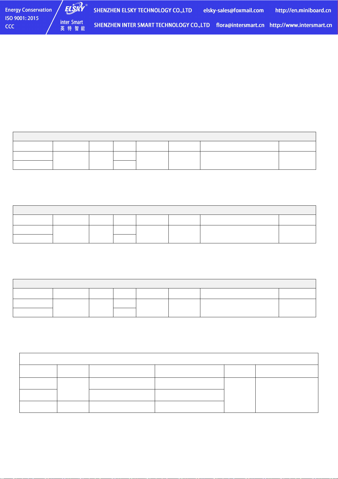
Chapter One The Motherboard specifications
Form Factor
Standard Thin-ITX,170*170*18mm(L*W*H)
Processor
EM218:Support Intel Celeron dual cores J1800 CPU;
EM219:Support Intel Celeron quad cores J1900 CPU;
EM229:Support Intel Pentium quad cores J2900 CPU.
Chipset
Intel Bay trail SOC Chipset
Cooling
Heat sink(Fanless,passive cooling);
Optional thin silent cool fan.
Supply
1*DC_JACK1 interface
DC port:5.5*2.5mm; Support 12V;
The motherboard full load power consumption is about 25W;
Recommend 12V 5A / 7A / 10A power adapter.
1*DC_PWR1 interface
Memory
1*SODIMM1 slot
1*NB-DDR3 1600MHz 1.35V Memory slot,Max. 8GB RAM.
Ethernet
1*RJ45 LAN interface
Realtek 8111H 10/100/1000Mbps RJ45 LAN port;
Wake-on-LAN and PXE diskless boot function.
1*MINI_PCIE interface
Support optional WIFI/Bluetooth/3G/4G/GPS,etc.
Display
Integrated Intel HD Graphics in CPU;
Support single display,dual display copy/expansion,single display in DOS.
1*VGA DB15 interface
Support Max. Resolution 1920*1200@60Hz
1*VGA_H1 pin
Support Max. resolution 1920*1200@60Hz (12Pin,1*12Pin,2.0mm)
1*EDP1 pin
Support Max. resolution 1920*1080@60Hz (30Pin,2*15Pin,2.0mm)
1*EDP1_PWR pin
EDP1 voltage control pin (3Pin,1*3Pin,2.54mm)
1*EDP2 pin
Support Max. resolution 1920*1080@60Hz (20Pin,2*10Pin,2.0mm)
1*LVDS2 pin
Support Max. resolution 1920*1080@60Hz (30Pin,2*15Pin,2.0mm)
1*LVDS_PWR2 pin
LVDS/EDP2 voltage control pin (6Pin,2*3Pin,2.0mm)
1*INVERT pin
LVDS/EDP2 backlight control pin (6Pin,1*6Pin,2.0mm)
USB
1*USB3.0 interface
Rear standard USB3.0 interface
3*USB2.0 interfaces
Rear standard USB2.0 interface
1*F_USB2 pin
Front USB2.0 pin;One group has 2*USB2.0 (9Pin,2*5Pin,2.54mm)
1*F_USB3 pin
Front USB2.0 pin;One group has 2*USB2.0 (9Pin,2*5Pin,2.54mm)
Sound
Integrated Realtek ALC662 HD digital audio decoder,6-channel high-fidelity audio controller.
1*LINE_OUT interface
Support Audio output
1*MIC_IN interface
Support Microphone input
1*JAMP1 pin
This is the amplifier pin. It supports 8Ω 5W speaker dual channel output.
(4Pin,1*4Pin,2.0mm)
1*F_AUDIO1 pin
Standard Audio pin (9Pin,2*5Pin,2.54mm)
Hard Disk
1*SATA1 interface
Standard SATA2.0 hard disk interface
1*MSATA slot
Mini SATA2.0(MSATA) SSD slot
1*SATA_PWR pin
It is hard disk power supply pin and can take the 5V,12V electricity.
(4Pin,1*4Pin,2.54mm)
Switch
1*F_PANEL1 pin
Switch, power supply light, hard disk light, restart pin.
(9Pin,2*5Pin,2.54mm)
Parallel Port
1*JLPT1 pin
Standard printer interface pin (25Pin,2*13Pin,2.0mm)
Serial Port
1*COM1 interface
Support standard RS232;Not support RS422/RS485
1*COM2/3/4 pin
Support standard RS232;Not support RS422/RS485. (9Pin,2*5Pin,2.54mm)
1*JPCOM1/2/3/4 pin
Control the 9th pin of the COM1/2/3/4 to choose optional 0V/5V/12V.
(6Pin,2*3Pin,2.0mm)
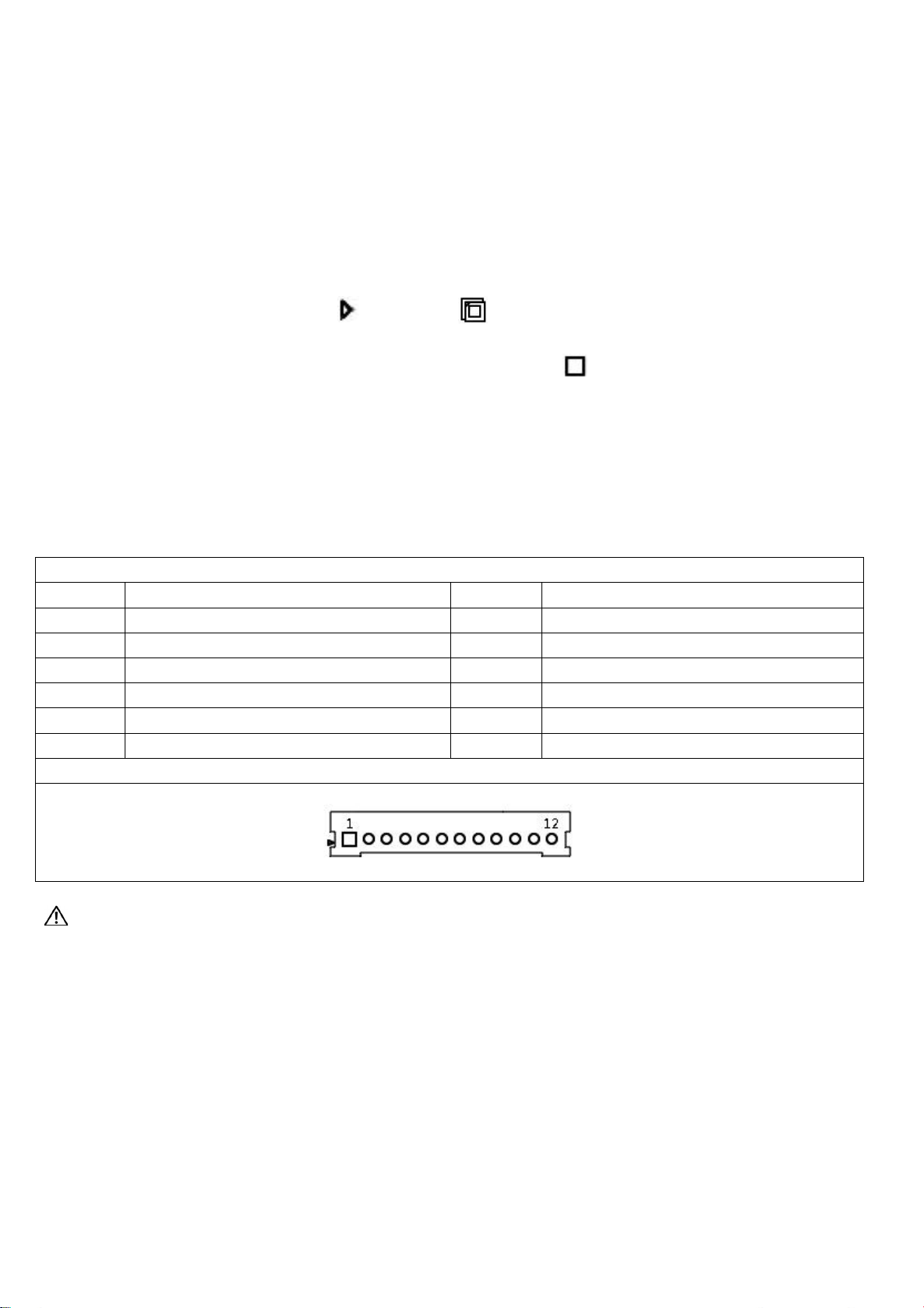
1*PS/2 pin
Standard PS/2 interface pin (7Pin,1*7Pin,2.0mm)
1*SIM_CARD1 slot
Support SIM card. A SIM card is required when using 3G/4G function.

- 4 -
Other I/O
1*CLR_CMOS1 pin
Motherboard discharges,clears pin. (3Pin,1*3Pin,2.54mm)
2*FAN pin
Fan pin (3Pin,1*3Pin,2.54mm)
1*J_GPIO1 pin
GPIO control pin (10Pin,2*5Pin,2.0mm)
Operating
Environment
Operating temperature:-20℃~60℃;
Working humidity:5%~95% Relative humidity, no condensation.
BIOS
AMI BIOS;Support power on,timing switch,remote switch,intelligently identify devices.
Watch Dog
Watch Dog programming supports hardware reset function (256 levels, 0~255 seconds).
Operating
System
Support Windows 10,Windows 8,Windows 7,Linux,etc.
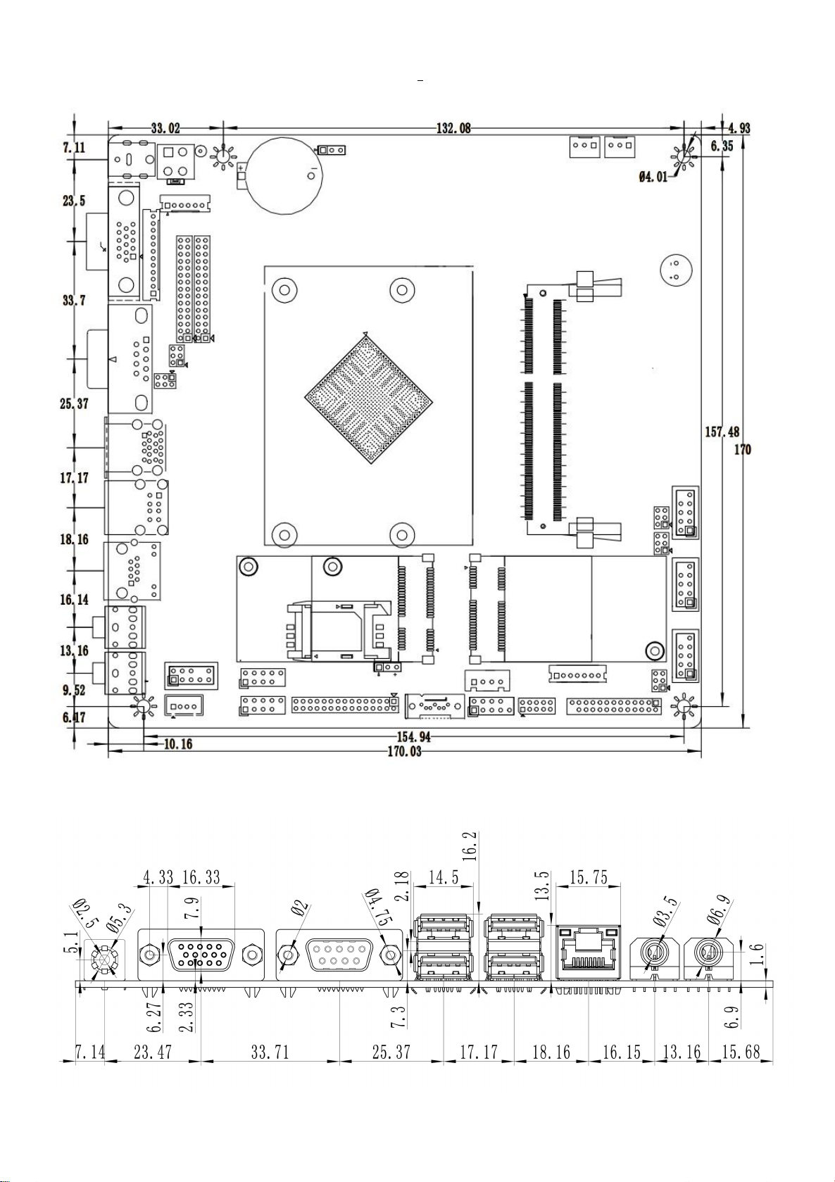
1.1 Motherboard Pictures:
4*COM:

- 5 -
2*COM:
- 6 -
1.2 The motherboard dimension drawing:
- 7 -
Chapter Two The motherboard pin definition and description
2.0 The 1st pin identification methods:
(1) Method 1: Look at the silkscreen mark next to the front pin of the motherboard.
Will be represented by a triangle symbol or a bold line or "1";
(2) Method 2: Look at the back pad of the motherboard. The square pad is the first pin;
Please pay attention to distinguish the 1st pin when plugging in the device and the cable, otherwise the motherboard
and device will be damaged.
2.1 VGA pin definition:
Position symbol: VGA_H1 (1*12Pin,2.0mm)
pin
definition
pin
definition
1
GND
2
VSYNC
3
HSYNC
4
GND
5
RED
6
GND
7
GRN
8
GND
9
BLUE
10
GND
11
DDC_DATA
12
DDC_CLK
pin position symbol drawing
Notice:The VGA_H1 pin signal is the same signal as the rear VGA port,and only support dual display copy.
- 8 -
2.2 LVDS pin definition:
Position symbol: LVDS2 (2*15Pin,2.0mm)
pin position symbol drawing
pin
definition
pin
definition
1
VCC
2
VCC
3
VCC
4
GND
5
GND
6
GND
7
ADO0-
8
ADO0+
9
ADO1-
10
ADO1+
11
ADO2-
12
ADO2+
13
GND
14
GND
15
ACLK-
16
ACLK+
17
ADO3-
18
ADO3+
19
BDO0-
20
BDO0+
21
BDO1-
22
BDO1+
23
BDO2-
24
BDO2+
25
GND
26
GND
27
BCLK-
28
BCLK+
29
BDO3-
30
BDO3+
Notice: When inserting the LVDS cable, the first pin of the LVDS cable must correspond to the first pin of the LVDS2
pin on motherboard. If the port is reversed or inserted incorrectly, there is a danger of burning the screen and burning
the motherboard!
2.3 EDP2 pin definition:
Position symbol: EDP2 (2*15Pin,2.0mm)
pin position symbol drawing
pin
definition
pin
definition
1
VCC
2
VCC
3
VCC
4
HPD
5
GND
6
GND
7
TX0N
8
TX0P
9
TX1N
10
TX1P
11
NC
12
NC
13
GND
14
GND
15
AUX-
16
AUX+
17
GND-
18
GND
19
TX2N
20
TX2P
Notice:
The EDP2 pin needs to connect independent backlight cable.
When inserting the EDP cable, the first pin of the EDP cable must correspond to the first pin of the EDP2 pin on
motherboard. If the port is reversed or inserted incorrectly, there is a danger of burning the screen and burning the
motherboard!

- 9 -
2.3.1 EDP2/LVDS backlight power supply definition:
Position symbol: INVERT (1*6Pin,2.0mm)
pin position symbol drawing
pin
definition
1
+12V
2
+12V
3
ON/OFF(Backlight switch)
4
ADJ(Backlight brightness adjustment)
5
GND
6
GND
2.3.2 EDP2/LVDS screen operating voltage:
Position symbol: LVDS_PWR2 (2*3Pin,2.0mm)
pin position symbol drawing
pin
definition
1-2 short circuit
+3.3V
3-4 short circuit
+5V
5-6 short circuit
+12V
Notice:Screens of different sizes require different operating voltages. The motherboard provides three screen
operating voltages of 3.3V, 5V and 12V. Please set the corresponding value of "LVDS_PWR2"according to the working
voltage required by the screen, otherwise there will be danger of burning the screen and burning the motherboard!
2.4 EDP1 pin definition:
Position symbol: EDP1 (2*15Pin,2.0mm)
pin position symbol drawing
pin
definition
pin
definition
1
VCC
2
VCC
3
GND
4
GND
5
TX0P
6
TX2P
7
TX0N
8
TX2N
9
GND
10
GND
11
TX1P
12
TX3P
13
TX1N
14
TX3N
15
GND
16
GND
17
AUXP
18
HPD
19
AUXN
20
NC
21
GND
22
GND
23
GND
24
GND
25
BKLT_EN
26
BKCTRL
27
VCC
28
VCC
29
VCC
30
NC
Notice:
EDP1 backlight cable and screen cable are two in one.
When inserting the EDP cable, the first pin of the EDP cable must correspond to the first pin of the EDP1 pin on
motherboard. If the port is reversed or inserted incorrectly, there is a danger of burning the screen and burning the
motherboard!

- 10 -
2.4.1 EDP1 screen operating voltage:
Position symbol: EDP1_PWR (1*3Pin,2.54mm)
pin position symbol drawing
pin
definition
1-2 short circuit
+3.3V
2-3 short circuit
+5V
Notice:Screens of different sizes require different operating voltages. The motherboard provides two screen
operating voltages of 3.3V, 5V. Please set the corresponding value of "EDP1_PWR"according to the working voltage
required by the screen, otherwise there will be danger of burning the screen and burning the motherboard!
2.5 LPT pin definition:
Position symbol: JLPT1 (2*13Pin,2.0mm)
pin position symbol drawing
pin
definition
pin
definition
1
STB
2
AFD
3
PD0
4
ERR
5
PD1
6
INIT
7
PD2
8
SLIN
9
PD3
10
GND
11
PD4
12
GND
13
PD5
14
GND
15
PD6
16
GND
17
PD7
18
GND
19
ACK
20
GND
21
BUSY
22
GND
23
PE
24
GND
25
SLCT
26
NC
2.6 Serial port(COM) function and pin definition:
The motherboard supports standard RS232 signal,does not support RS422/RS485.
The 9th pin of the COM1/COM2 /COM3/COM4 can change the jumper setting to output +5V or +12V voltage by
JPCOM1/JPCOM2/JPCOM3/JPCOM4.
Position symbol: JPCOM1 JPCOM2 JPCOM3 JPCOM4 (2*3Pin,2.0mm)
pin position symbol drawing
pin
The 9th pin of COM1/COM2/COM3/COM4 is charged
1-2 short circuit
+5V
3-4 short circuit
+12V
5-6 short circuit
Without electricity(Default)

- 11 -
COM1/2/3/4 definition:
Position symbol: COM2 COM3 COM4 (2*5Pin,2.54mm)
pin position symbol drawing
pin
definition
pin
definition
1
DCD
2
RXD
3
TXD
4
DTR
5
GND
6
DSR
7
RTS
8
CTS
9
RI
10
NC
COM1
interface
2.7 USB pin definition:
Position symbol: F_USB2 F_USB3 (2*5Pin,2.54mm)
pin position symbol drawing
pin
definition
pin
definition
1
VCC+5V
2
VCC+5V
3
DATA0-
4
DATA1-
5
DATA0+
6
DATA1+
7
GND
8
GND
9
NC
10
GND
2.8 Audio interface and pin definition:
Position symbol: F_AUDIO1 (2*5Pin,2.54mm)
pin position symbol drawing
pin
definition
pin
definition
1
MIC-L
2
GND
3
MIC-R
4
NC
5
LINE OUT-R
6
MIC_JD
7
FAUDIO_JD
8
NC
9
LINE OUT-L
10
LINE_JD
2.9 Speaker(Power Amplifier) pin definition:
Position symbol: JAMP1 (1*4Pin,2.0mm)
pin position symbol drawing
pin
definition
1
L+
2
L-
3
R-
4
R+

- 12 -
2.10 Power supply and switch pin definition:
The motherboard provides a standard 5.5*2.5mm DC port (DC_JACK1),1*4PIN ATX power supply interface.
4PIN ATX definition:
Position symbol: DC_PWR1 (2*2Pin)
pin position symbol drawing
pin
definition
1
GND
2
GND
3
+12V
4
+12V
Switch pin definition:
Position symbol: F_PANEL1 (2*5Pin,2.54mm)
pin position symbol drawing
pin
definition
pin
definition
1
HDLED+
Hard disk LED
2
PWRLED+
Power supply LED
3
HDLED-
4
GND
5
RST
Restart
6
P_SW IN
Switch
7
GND
8
GND
9
GND
10
NC
(1)Hard disk indicator light:
The 1st and 3rd pins are HDDLED. The 1st pin is the positive side of the LED.When the hard disk is being read or
written,the indicator light will flash, indicating that the hard disk is running.
(2)Power supply indicator light:
The 2nd and 4th pins are Power LED. The 2nd pin is the positive side of the LED.When the motherboard is powered
on,the power indicator light is on.When the motherboard is powered off, the power indicator light is off.
(3)Restart button:
The 5th,7th pins are Restart Buttons.When the system fails and cannot continue to work, the restart can restart the
system.
(4)Power supply switch control:
The 6th, 8th pins are power supply buttons.Using these two pins to connect to the bounce switch on the front panel of
the chassis to turn on or off the computer.
2.11 PS/2 pin definition:
Position symbol: PS/2 (1*7Pin,2.0mm)
pin position symbol drawing
pin
definition
1
K_SATA
2
K_CLK
3
GND
4
M_DATA
5
M_CLK
6
GND
7
+5V

- 13 -
2.12 Fan interface definition:
Position symbol: FAN1 FAN2 (1*3Pin,2.54mm)
pin position symbol drawing
pin
definition
1
GND
2
+12V
3
TAC(Fan speed detection)
2.13 Hard disk interface and definition:
The motherboard provides:
1*SATA2.0 hard disk interface;
1*MSATA2.0 slot;
1*4Pin hard disk power supply voltage interface.
SATA definition:
Position symbol: SATA1
pin
definition
1
GND
2
SATA_TXP
3
SATA_TXN
4
GND
5
SATA_RXN
6
SATA_RXP
7
GND
SATA_PWR definition:
Position symbol: SATA_PWR (1*4Pin,2.54mm)
pin position symbol drawing
pin
definition
1
12V
2
GND
3
GND
4
5V
Notice:The first pin of the"SATA_PWR"hard disk power supply interface is 12V output, and the fourth pin is 5V
output. When using, you must use the customized power cord from our company to avoid burning the hard disk.

- 14 -
2.14 Motherboard discharges,clears and battery:
The"CMOS" is powered by the button battery on the motherboard.
Clearing the "CMOS" will cause the previous BIOS settings to be cleared and restore the original factory setting.
Clearing CMOS procedures:
Method 1:
(1)Turn off the motherboard and disconnect the power.
(2)Use metal conductors to briefly connect the pin 2,pin 3 of "CLR_CMOS1" for 5~6 seconds.
(3)When booting up, press "Delete" to enter the BIOS.
(4)After entering the BIOS, press "F9" ,"Enter" to reload the optimal default value.
(5)Press the "F10" to save and exit the setting.
Method 2:
When the motherboard is powered off, plug and pull the button battery to achieve the motherboard clear function.
Remove the button battery, and then re-install the button battery after 10 seconds.Please pay attention to the positive
and negative of the battery.
CMOS pin definition:
Position symbol: CLR_CMOS1 (1*3Pin,2.54mm)
pin position symbol drawing
pin
Function
1-2 short circuit
Normal
2-3 short circuit
Clear CMOS content,BIOS will restore factory settings.
Notice: Please do not clear the"CMOS"when the motherboard is running or charging, so as not to damage the
motherboard.
Button battery specification: 3V CR2032
Notice:
(1) Please make sure the battery is facing up.
(2) Please make sure the battery voltage is enough 2.8V~3V.
(3) Please must use the same model or the manufacturer recommend the same type of battery.
(4) If the battery is not replaced correctly, there is a danger of explosion!

- 15 -
Chapter Three BIOS Setup
BIOS hot key
Function
When starting, press the "Delete" button
Enter "BIOS"
When starting, press the "F11" button
Select"Setup",or select enter"BIOS".
← →
Select Screen(Move the left and right arrows to select an entry).
↑ ↓
Select Item(Move the up and down arrows to select an entry).
Enter
Select(Select item and enter the submenu).
+/-
Change Opt.(Change selections,add or subtract values).
F1
General help(Show related help content).
F9
Optimized Defaults(Go back to the vendor's default settings).
F10
Save&Exit
Esc
Exit
3.0 How to enter the BIOS?
Method 1 : After starting, press"Delete"continuously to enter the BIOS directly.
Method 2 : Press"F11"continuously after booting, then select "Enter Setup"to enter the BIOS.

- 16 -
3.1 Main Menu(BIOS information):
(1) BIOS Vendor: American Megatrends
(2) Project Version: EM219-2C x64
(3) Build Date and Time: 08/14/2019 11:27:43
(4) Processor Information: CPU model
(5) Memory Information:
(6) OS Selection: It is operating system options,you can choose Windows 7 / Linux / Windows 8.X
Windows 7: Windows 7
Linux: Android
Windows 10: Windows 8.X
(7) System Date: The format is week Month/day/year
(8) System Time: The format is hour/minute/second
- 17 -
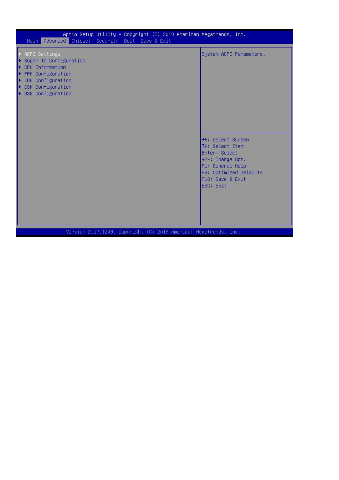
3.2 Advanced:
(1) ACPI Settings: Advanced configuration and power supply management interface setting.
(2) Super IO Configuration:
(3) CPU Information: CPU parameter information and common setting options
(4) PPM Configuration:
(5) IDE Configuration: Hard disk mode settings and information
(6) CSM Configuration:
(7) USB Configuration: USB information and control options

- 18 -
3.2.1 ACPI Settings(C-state Settings): C-State : Disabled
(1)Enable ACPI Auto Configuration:
This item is ACPI automatically configured. It can"Enabled"or"Disabled"the ACPI auto configuration of the BIOS.By
default, the motherboard is set to"Disabled".
(2)Enable Hibernation:
This item is hibernation support. It can "Enabled"or"Disabled"the system hibernation function(In OS/S4 sleep
state).However, this option does not work in some operating systems. By default, the motherboard is set to"Enabled".
(3)ACPI Sleep State:
This item is used to select the power saving mode when the system sleeps.The mode is different, the system power
consumption will be different.
Suspend Disabled: Turn off sleep mode.
S1(CPU Stop Clock): The CPU stops working, but the other devices are still powered normally.
S3(Suspend to Ram): Suspend to memory.
(4)Lock Legacy Resources:
It can"Enabled"or"Disabled"legacy resources lock.
(5)Wake up By PCIE LAN:
This is the"Wake on LAN"switch.The"Disabled"is turn off; The"Enabled"is turn on.

- 19 -
3.2.2 Set the Power on/off function in BIOS:
Restore AC Power Loss: It is the"power on/off"switch in BIOS.
Power Off : After the motherboard is powered,it won't automatically boot and you need to boot it manually.
Power On: After the motherboard is powered,it will automatically boot and you don't need to boot it manually.
By default,the motherboard is set to "Power Off".
3.2.3 Timed boot settings:
Resume On RTC Alarm: It is timed booting setting(Automatically start operating system in fixed time).
The"Disabled" is turn off; The"Enabled"is turn on.
RTC Alarm Date(Days)
RTC Alarm Time(Hours)
RTC Alarm Time(Minutes)
RTC Alarm Time(Seconds)

- 20 -
3.2.4 Super IO Configuration:
(1) Serial Port 1 Configuration: It is COM1 configuration information and settings. Only support RS232.
(2) Serial Port 2 Configuration: It is COM2 configuration information and settings. Only support RS232.
(3) Serial Port 3 Configuration: It is COM3 configuration information and settings. Only support RS232.
(4) Serial Port 4 Configuration: It is COM4 configuration information and settings. Only support RS232.
(5) Parallel Port Configuration:It is LPT configuration information and settings.
(6) Watch dog Controller:This is the watch dog setting.
This manual suits for next models
8
Table of contents
Other ELSKY Motherboard manuals


Popular Motherboard manuals by other brands


Texas Instruments
Texas Instruments TPS65053EVM-389 user guide

Texas Instruments
Texas Instruments ADCx140EVM-PDK Series user guide

ASROCK
ASROCK IMB-155B user manual

Analog Devices
Analog Devices EVAL-SSM3582Z user guide

AOpen
AOpen i945GTm-VHL manual

Linear Technology
Linear Technology DC2017A Demo Manual