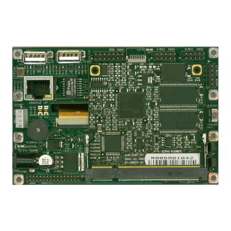
EMAC SoM-A5D36 User manual

SoM-A5D36
User Manual
April 2019
Revision 1.30
Copyright © 2015
EMAC, Inc.
2390 EMAC Way, Carbondale, Illinois 62902
Phone: (618) 529-4525 Fax: (618) 457-0110
http://www.emacinc.com

SoM-A5D36 User Manual
Revision 1.30 © 2015 - 1 -
Table of Contents
1Introduction........................................................................................................................................................... - 4 -
1.1....Features............................................................................................................................................................................. - 4 -
2Hardware ................................................................................................................................................................ - 5 -
2.1....Specifications .................................................................................................................................................................. - 5 -
2.2....Real-Time Clock.............................................................................................................................................................. - 7 -
2.3....Watchdog Timer............................................................................................................................................................ - 7 -
2.4....External Connections ................................................................................................................................................... - 7 -
2.4.1External Bus ..............................................................................................................................................................................- 8 -
2.4.2JTAG .............................................................................................................................................................................................- 9 -
2.4.3One-Wire / I2C .........................................................................................................................................................................- 9 -
2.4.4Ethernet................................................................................................................................................................................... - 10 -
2.4.5USB............................................................................................................................................................................................ - 11 -
2.4.6SPI.............................................................................................................................................................................................. - 12 -
2.4.7MCI Multimedia Card ......................................................................................................................................................... - 13 -
2.4.8Serial Ports.............................................................................................................................................................................. - 14 -
2.4.9I2S.............................................................................................................................................................................................. - 15 -
2.4.10 CAN.................................................................................................................................................................................... - 15 -
2.4.11 GPIO.................................................................................................................................................................................. - 16 -
2.4.12 Interrupts......................................................................................................................................................................... - 17 -
2.4.13 ADC .................................................................................................................................................................................... - 17 -
2.4.14 Timer/Counters ............................................................................................................................................................. - 18 -
2.4.15 SoM Status LED.............................................................................................................................................................. - 18 -
2.4.16 LCD..................................................................................................................................................................................... - 19 -
2.4.17 Additional Interfaces................................................................................................................................................. - 20 -
2.5....Power Connections.....................................................................................................................................................- 21 -
2.6....Boot Options..................................................................................................................................................................- 21 -
2.7....Serial Data Flash..........................................................................................................................................................- 22 -
3Design Considerations......................................................................................................................................- 22 -
3.1....Off-the-Shelf Carriers.................................................................................................................................................- 22 -
3.1.1SoM-200GS............................................................................................................................................................................. - 22 -
3.1.2SoM-250GS............................................................................................................................................................................. - 23 -

SoM-A5D36 User Manual
Revision 1.30 © 2015 - 2 -
3.2....Semi-Custom Carriers ..............................................................................................................................................- 23 -
3.3....Designing Your Own Carrier.................................................................................................................................- 23 -
3.3.1Power ...................................................................................................................................................................................... - 23 -
3.3.2Analog Reference ............................................................................................................................................................... - 24 -
3.3.3Battery Backup.................................................................................................................................................................... - 24 -
3.3.4Shutdown Logic Pins ........................................................................................................................................................ - 24 -
4Software................................................................................................................................................................- 25 -
4.1....Das U-Boot.....................................................................................................................................................................- 25 -
4.2....Embedded Linux...........................................................................................................................................................- 25 -
4.2.1Linux with Xenomai Real Time Extensions.................................................................................................................. - 25 -
4.2.2Linux Packages ...................................................................................................................................................................... - 26 -
4.2.3Linux Patches......................................................................................................................................................................... - 26 -
4.3....Qt Creator.......................................................................................................................................................................- 26 -
4.4....ARM EABI Cross Compiler...................................................................................................................................- 26 -

SoM-A5D36 User Manual
Revision 1.30 © 2015 - 3 -
Disclaimer
EMAC Inc. does not assume any liability arising out of the application or use of any of its products
or designs. Products designed or distributed by EMAC Inc. are not intended for, or authorized to
be used in, applications such as life support systems or for any other use in which the failure of
the product could potentially result in personal injury, death or property damage.
If EMAC Inc. products are used in any of the aforementioned unintended or unauthorized
applications, Purchaser shall indemnify and hold EMAC Inc. and its employees and officers
harmless against all claims, costs, damages, expenses, and attorney fees that may directly or
indirectly arise out of any claim of personal injury, death or property damage associated with
such unintended or unauthorized use, even if it is alleged that EMAC Inc. was negligent in the
design or manufacture of the product.
EMAC Inc. reserves the right to make changes to any products with the intent to improve overall
quality, without further notification.

SoM-A5D36 User Manual
Revision 1.30 © 2015 - 4 -
1Introduction
This document describes EMAC’s SoM-A5D36 System on Module (SoMs). The SoM-A5D36 is a System on
Module, designed to be compatible with EMAC’s 200-pin SODIMM form factor. This module is built
around the ATSAMA5D36 ARM based microcontrollers, which provides several of its key features.
The SoM-A5D36 has an onboard Gigabit Ethernet PHY, 6 serial ports, an RTC, onboard eMMC flash, Serial
NOR Flash, and SDRAM. In addition to the standard SoM features, the SoM-A5D36 also features a fast
32-bit core, open source software support, and a wide range of controller I/O pins.
1.1 Features
▪Small, 200 pin SODIMM form factor (2.66" x 2.384")
▪Atmel ARM Cortex-A5 ATSAMA5D36 536MHz Processor
▪10/100/1000 BaseT Ethernet with on-board PHY
▪RMII Interface for additional 10/100 BaseT PHY
▪6 Serial ports, one with full handshake and 3 with RTS/CTS handshake
▪2 USB 2.0 (High Speed) Host port
▪1 USB 2.0 (High Speed) OTG Host/Device port
▪Up to 512 MB of LPDDR2 SDRAM
▪4 GB of eMMC Flash
▪16 MB of NOR Serial Flash
▪2 SD/MMC Flash Card Interfaces
▪Battery-backed Real-Time Clock
▪2 SPI ports
▪2 I2C ports
▪1 I2S Audio port
▪2 CAN ports
▪6-Channel 12-bit Analog-to-Digital converter with 4-wire Touchscreen Interface
▪Image Sensor Interface (ISI), ITU-R BT. 601/656
▪Timer/Counters and Pulse Width Modulation (PWM) ports
▪Graphic LCD Interface with 2D acceleration with 2048x2048 Resolution or up to 720p
▪32-bit True Random Number Generator
▪Typical power requirement less than 1 Watt
▪JTAG for debug, including real-time trace
▪FREE Qt Creator IDE with GCC & GDB development tools

SoM-A5D36 User Manual
Revision 1.30 © 2015 - 5 -
2Hardware
2.1 Specifications
▪CPU: Embedded Atmel ATSAMA5D36 processor running at 536MHz
▪Flash: 4GB eMMC Flash and 16MB of Serial Data Flash.
▪RAM: 512 MB 133 MHz LPDDR2.
▪Flash Disk: 4-bit SDHC/MMC interface.
▪System Reset: Supervisor with external Reset Button provision.
▪RTC: Real-Time Clock/Calendar with battery-backed provision using 32-bit free-running counter.
▪Timer/Counters: 5, 2-channel, 32-bit timers/counters with capture, compare, and PWM.
▪PWM: 4 PWM channels, one with complimentary outputs.
▪Watchdog Timer: External Watchdog Timer (MAX6747).
▪Digital I/O: 32 General Purpose I/Os with 16 mA drive when used as an output
▪Analog I/O: 6-channel, 12-bit Analog-to-Digital converter (ADC)
▪Power: Power Management Controller allows selectively shutting down on-processor I/O
functionality and running from a slow clock.
▪JTAG: JTAG for debug, including real-time trace.
▪CLOCKS: PLL synthesized 8MHz, 200KHz, 14.3MHz clock outputs
Serial Interfaces
▪UARTS: 6 serial TTL level serial ports with Auto RS485 and most with handshaking
(each UART requires external RS level shifting).
▪SPI: 2 High-Speed SPI ports with Chip Selects.
▪Audio: I2S Synchronous Serial Controller with analog interface support
▪USB: Dual USB 2.0 High Speed Host and single USB 2.0 High Speed Device ports
▪I2C: Two I2C ports

SoM-A5D36 User Manual
Revision 1.30 © 2015 - 6 -
Ethernet Interface
▪MAC: ATSAMA5D36 on chip MAC
▪PHY: Micrel KSZ9031 Gigabit PHY with software shutdown.
▪Interface: IEEE 802.3u 10/100/1000 BaseT Fast Ethernet (requires external magnetics and Jack)
Bus Interface:
▪Local Bus accessible through SODIMM provides 22 address lines, 16 data bus lines, and control
lines.
Mechanical and Environmental
▪Dimensions: SODIMM form factor with the length dimension extended (2.66" x 2.384")
▪SODIMM TYPE: 200 Pin DDR1 (not compatible with DDR2)
▪Power Supply Voltage: +3.3 Volts DC +/- 5%
▪Power Requirements (Typical):
▪3.3 Volts @ 300 mA (less than 1 watt)
▪Max current draw during boot process: 340 mA
▪Constant busy loop: 260 mA
▪Idle system: 245 mA
▪Idle system with Ethernet PHY disabled: TBD
▪Operating Temperature: -40 to 85° C (-40 to 185 ° F), fanless operation
▪Operating Humidity: 0% to 90% relative humidity, non-condensing

SoM-A5D36 User Manual
Revision 1.30 © 2015 - 7 -
2.2 Real-Time Clock
The SoM-A5D36 has an embedded Real-time Clock. Battery backup is provided from the carrier board
using the VSTBY pin. The SoM-A5D36 will retain the RTT value register during reset and hence use it as an
RTC. The RTC has the provision to set alarms that can interrupt the processor. For example, the processor
can be placed in sleep mode and then later awakened using the alarm function.
2.3 Watchdog Timer
The SoM-A5D36 provides an external Watchdog Timer/ Supervisor (MAX6747) with an extended
watchdog timeout period of 1.42 seconds (±10%). Upon power-up the Watchdog is disabled and does not
require pulsing. To start the Watchdog, it must first be enabled. This is done by configuring port line PD8
as an output and setting it low in software. Once enabled, the Watchdog should be pulsed, using port line
PD6, continually every 1.28 seconds or faster to prevent the Watchdog from timing out and resetting the
module. If you are using the watchdog to force a system reset, you may need up to 1.56 seconds of
inactivity before the Watchdog reset will occur. The watchdog is automatically disabled upon reset but it
can also be disabled by setting PD8 high.
2.4 External Connections
The SoM-A5D36 connects to a carrier board containing its connectors, power supply and any expansion
IO, through a standard ENIG-plated (Electroless Nickel Immersion Gold) SODIMM 200-pin connection
shown below.
The SoM model will fit in any standard 200-pin SODIMM socket. These connections are designed to be
compatible with all EMAC 200-pin SoM products. See EMAC SoM 200-pin SODIMM Pinout Specification
to see how other 200-pin SoM pinouts line up with the SoM-A5D36’s pinout.
The use of the DDR SODIMM form-factor for EMAC’s SoMs is a sound choice that has been proven rugged
and reliable in the laptop and embedded SBC markets.
The remainder of this section describes the pinout as it applies specifically to the SoM-A5D36 processor.

SoM-A5D36 User Manual
Revision 1.30 © 2015 - 8 -
2.4.1 External Bus
The SoM-A5D36 provides a flexible external bus for connecting peripherals. The CPLD of the SoM-200GS
and SoM-250GS connect through a subset of these connections. The WKUP pin has a Maximum input
voltage of 3.3V (pulled up on-module to 3.3V) and Shutdown has a maximum output voltage of 3.3V. The
Flash WP for the Serial Flash is active-low and pulled up on-module.
Table 1: External Bus Interface
SODIMM
Pin#
SoM
Pin Name
Processor
Pin Name(s)
Port Line
Description
145
GP_CSA
NCS1
PE27
General Purpose Chip Select CS0
146
GP_CSB
NCS2
PE28
General Purpose Chip Select CS4
147
GP_CSC
NCS3
N/A
General Purpose Chip Select CS2
148
GP_CSD/Shutdown
PWRDN
N/A
Processor Shutdown Output
149
WR
NWE
N/A
Write Signal
150
RD
NRD
N/A
Read Signal
151
RST_IN
NRST
*
Processor Reset
152
RST_OUT
~RST_OUT
*
Processor Reset
153
WAIT
NWAIT
PE30
Shutdown Control
154
~FLASH WP
*
*
Serial Flash Write Protect
54
WAKEUP
WKUP
N/A
Processor Wakeup Input
157
BOOT_OPTION0
BMS
N/A
Boot0 Option Select
158
BOOT_OPTION1
*
*
Boot1 Option Select
175-193
A0 –A18
A0 –A18
PE0-PE18
Address Bus
194
A19
A19
PE19
Address Bus line A19
195
A20
A20
PE20
Address Bus line A20
196
A21
A21
PE21
Address Bus line A23
159-174
D0 - D15
D0 –D15
N/A
Data Bus
*The RST_IN pin is an active low input that drives the processor reset pin. The RST_OUT pin is an active
low output that is driven low by either the watchdog timer or a software reset. The ~FLASH_WP pin is an
active low input that prevents the serial NOR flash from being written to. The BOOT_OPTION1 pin is an
input that disables the serial NOR flash.

SoM-A5D36 User Manual
Revision 1.30 © 2015 - 9 -
2.4.2 JTAG
The SoM specification allows for access to the JTAG lines for the ATSAMA5D36 processor. These
connections will allow the Flash to be programmed in circuit via a program running from the processor
and also the capability to debug software.
Table 2: Processor JTAG
SODIMM
Pin#
SoM
Pin Name
Processor
Pin Name(s)
Description
139
JTAG_TCK
JTAG_TCK
JTAG Clock
140
JTAG_TDI
JTAG_TDI
JTAG Serial In
141
JTAG_TDO
JTAG_TDO
JTAG Serial Out
142
JTAG_TMS
JTAG_TMS
JTAG Operation Mode
143
JTAG_TRST
JTAG_TRST
Test Reset Signal
144
JTAG_RTCK
NC
Dynamic Clock Sync
2.4.3 One-Wire / I2C
The SoM-200 specification calls for a two-wire I2C port. The SoM-A5D36 does not have a native hardware
One-Wire port but does provide general purpose lines that can be used in this capacity when “bit-banged”.
Both Linux and CE provide this functionality.
Table 3: One-Wire / I2C Port
SODIMM
Pin#
SoM
Pin Name
Processor
Pin Name(s)
Port Line
Description
29
I2CCLK
TWCK0
PA31
Clock Pin
30
I2CDATA
TWD0
PA30
Data Pin
There is an additional available I2C interface that is shared with the USB OTG pins. This additional port
can be utilized on a custom carrier board.
Table 4: Additional I2C Port
SODIMM
Pin#
SoM
Pin Name
Processor
Pin Name(s)
Port Line
Description
10
USB_OTG_VBUS
TWCK1
PC27
Clock Pin
40
USB_OTG_ID
TWD1
PC26
Data Pin

SoM-A5D36 User Manual
Revision 1.30 © 2015 - 10 -
2.4.4 Ethernet
The SoM-A5D36 provides a Micrel KSZ9031 10/100/1000 Ethernet PHY IC on board. Carrier designers need
only run these lines through the appropriate magnetics layer to have a functional Ethernet connection.
Remember the RX and TX lines are differential pairs and need to be routed as such.
The LED/configuration pins’ state at reset determines the PHY address. These pins are pulled to set the
PHY address to 0x01 by default. The address can be changed by pulling these lines to a different value on
a custom carrier board. This can be especially useful if an additional PHY is added to a custom carrier by
accessing the RMII pins described below.
Table 5: Ethernet
SODIMM
Pin#
SoM
Pin Name
KSZ9031
Pin Name
Description
12
GIG D-
TXRXD_N
GIG Ethernet D- pin
14
GIG D+
TXRXD_P
GIG Ethernet D+ pin
13
GIG C-
TXRXC_N
GIG Ethernet C- pin
15
GIG C+
TXRXC_P
GIG Ethernet C+ pin
16
Ethernet_Rx-/GIG B-
TXRXB_N
Low differential Ethernet receive
line
18
Ethernet_Rx+/GIG B+
TXRXB_P
High differential Ethernet receive
line
17
Ethernet_Tx-/GIG A-
TXRXA_N
Low differential Ethernet transmit
line
19
Ethernet_Tx+/GIG A+
TXRXA_P
High differential Ethernet transmit
line
38
LED_LINK/CFG_2
LED2/PHY_AD1
Ethernet Link LED/Configuration
pin
39
LED_ACT/CFG_3
LED1/PHY_AD0
Ethernet Activity LED/Configuration
pin
Table 6: RMII Ethernet Interface
SODIMM
Pin#
SoM
Pin Name
Processor
Pin Name
Description
99
COMA_DTR
ETX0
RMII Transmit Data 0
100
COMA_DSR
ETX1
RMII Transmit Data 1
101
COMA_RI
ERX0
RMII Receive Data 0
104
COMB_CTS
ERX1
RMII Receive Data 1
105
COMB_RTS
ETXEN
RMII Transmit Control
37
Card_Detect
ECRSDV
RMII Receive Control
116
GPIO2
ERXER
RMII Receive Error
117
GPIO3
EREFCK
RMII Reference Clock
118
GPIO4
EMDC
RMII Management Data Clock
119
GPIO5
EMDIO
RMII Management Data IO

SoM-A5D36 User Manual
Revision 1.30 © 2015 - 11 -
2.4.5 USB
The SoM 200-pin specification provides for 2 USB hosts and 1 USB device or OTG (On-The-GO) port. The
SoM-A5D36 does provide a USB OTG-like port. EMAC has mapped this port to both Host A and Device A
ports. This allows the port to be used as a Full time Host port by connection to Host A or for a full time
Device port by connection to device Port A. The use of Port A also allows for USB OTG in conjunction with
VBUS and ID signals. There is a GPIO line that can be utilized to enable USB power if necessary. This is SoM
pin# 125, GPIO11 and is not required if power will always be on. Remember the USB Data lines are
differential pairs and need to be routed as such.
Table 7: USB
SODIMM
Pin#
SoM
Pin Name
Processor
Pin Name(s)
Port Line
Description
5
Host_A+
HHSD2_P
N/A
Host USB 2.0 PortB +
7
Host_A-
HHSD2_N
N/A
Host USB 2.0 PortB -
6
Host_B+
HHSD3_P
N/A
Host USB 2.0 PortC +
8
Host_B-
HHSD3_N
N/A
Host USB 2.0 PortC -
9
Host/Device/OTC_C-
H/D_HSD1_N
N/A
OTG USB 2.0 PortA -
11
Host/Device/OTG_C+
H/D_HSD1_P
N/A
OTG USB 2.0 PortA +
10
USB_OTG_VBUS
PC27/SPI1_NPCS2/TWCK1
N/A
OTG VBUS
40
USB_OTG_ID
PC26/SPI1_NPCS1/TWD1
N/A
OTG ID

SoM-A5D36 User Manual
Revision 1.30 © 2015 - 12 -
2.4.6 SPI
The ATSAMA5D36 processor provides two SPI (Serial Peripheral Interface) channels, SPI0 and SPI1, for
communicating with peripheral devices. The SPI0 bus is connected internally to the serial flash, which uses
SPI0_NPCS0 (SPI0_NPCS0 is not brought out to the card fingers). Table 8 below lists the lines for SPI
channel 0. Table 9 below lists the lines for the SPI channel 1. These pins have shared functions and can
be accessed through the GPIO header on the SoM-200 carrier board. Note SPI Chip Selects (CS) for both
Linux & WinCE do not require a specific SPI_CS and as such can use any GPIO allowing additional chip
selects if a custom carrier is used.
Table 8: SPI Channel 0
SODIMM
Pin#
SoM
Pin Name
Processor
Pin Name(s)
Port Line
Description
22
SPI_MI
SPI0_MISO
PD10
SPI0 serial data in
23
SPI_MO
SPI0_MOSI
PD11
SPI0 serial data out
24
SPI_SCK
SPI0_SPCK
PD12
SPI0 serial clock out
25
SPI_CS0
SPI0_NCS1/CANRX0
PD14
SPI0 slave select line 0
26
SPI_CS1
SPI0_NCS2/CANTX0
PD15
SPI0 slave select line 1
27
SPI_CS2
SPI0_NCS3
PD16
SPI0 slave select line 2
28
SPI_CS3
SPI0_NCS4/PWMFI2
PC28
SPI0 slave select line 3
Table 9: SPI Channel 1
SODIMM
Pin#
SoM
Pin Name
Processor
Pin Name(s)
Port Line
Description
126
GPIO12
SPI1_MISO
PC22
SPI1 serial data in
127
GPIO13
SPI1_MOSI
PC23
SPI1 serial data out
128
GPIO14
SPI1_SPCK
PC24
SPI1 serial clock out
134
GPIO15
SPI1_NCS0
PC25
SPI1 slave select line 0
40
USB_OTG_ID
SPI1_NCS1
PC26
SPI1 slave select line 1
10
USB_OTG_VBUS
SPI1_NCS2
PC27
SPI1 slave select line 2

SoM-A5D36 User Manual
Revision 1.30 © 2015 - 13 -
2.4.7 MCI Multimedia Card
The SoM-A5D36 provides two 4-bit MMC/SD card interfaces, MCI1 and MCI2. The SoM-200 specification
provides for three associated but optional SD/MMC control lines. Since these lines are optional and will
not always be used they are not part of the SD/MMC group but are part of the GPIO group. SoM pin#s
122, 123, and 124 can be used as SD_LED, SD_Power, and SD_protect, respectively.
MCI1 is allocated to the SoM Pin Specification in the SD/MMC section as the default SD port. When
designing a custom carrier, MCI1 should be used rather than MCI2 if you want to maintain compatibility
with present and future SoMs. The SoM-200GS/250GS Carrier boards’ memory sockets make use of MCI1.
The MCI2 interface should only be used if you are not concerned about compatibility with existing and
future SoMs. MCI2 is accessed through the SoM-A5D36’s GPIO section.
Table 10: MMC/SD Card Interface
SODIMM
Pin#
SoM
Pin Name
Processor
Pin Name(s)
Port Line
Description
31
SDCLK
MCI1_CLK
PB24
MCI Clock
32
CMD
MCI1_CDA
PB19
MCIB Command
33
DAT0
MCI1_DA0
PB20
MCIB D0
34
DAT1
MCI1_DA1
PB21
MCIB D1
35
DAT2
MCI1_DA2
PB22
MCIB D2
36
DAT3
MCI1_DA3
PB23
MCIB D3
37
Card_Detect
PC5/TCLK4
PC5
Card Detect
An additional MMC/SD interface is available through shared GPIO lines. All the lines for the second
MMC/SD port are brought out to a header on the SoM-200 carrier.
Table 11: Additional MMC/SD Card Interface
SODIMM
Pin#
SoM
Pin Name
Processor
Pin Name(s)
Port Line
Description
125
GPIO11
MCI2_CK/PCK2
PC15
MCI Clock
120
GPIO6
MCI2_CDA
PC10
MCIC Command
121
GPIO7
MCI2_DA0
PC11
MCIC D0
122
GPIO8
MCI2_DA1/TIOA1
PC12
MCIC D1
123
GPIO9
MCI2_DA2/TIOB1
PC13
MCIC D2
124
GPIO10
MCI2_DA3/TCLK1
PC14
MCIC D3

SoM-A5D36 User Manual
Revision 1.30 © 2015 - 14 -
2.4.8 Serial Ports
The SoM-200 pin specification has the provision for 4 serial ports. However, the ATSAMA5D36 provides 6
serial ports. The additional serial ports are accommodated through the use of alternate SoM pins. COMB
(Debug port) is normally the console port. The ATSAMA5D36 processor does not provide full modem
handshaking for COMA as called for in the SoM-200 pin specification, therefore EMAC has utilized
processor GPIO lines for this function. The RTS lines for each port can be used to achieve automatic RS485
direction control.
Table 12: Serial Ports
SODIMM
Pin#
SoM
Pin Name
Processor
Pin Name(s)
Port Line
SoM Description
95
COMA_TXD
TXD1
PB29
COMA transmit/GPIO
96
COMA_RXD
RXD1
PB28
COMA receive/GPIO
97
COMA_CTS
CTS1
PB26
COMA CTS/GPIO
98
COMA_RTS
RTS1
PB27
COMA RTS/GPIO
99
COMA_DTR
PC0/TIOA3
PC0
COMA DTR/GPIO
100
COMA_DSR
PC1/TIOB3
PC1
COMA DSR /GPIO
101
COMA_RI
PC2/TCLK3
PC2
COMA RING/GPIO
102
COMB_TXD
DTXD
PB31
COMB transmit/GPIO
103
COMB_RXD
DRSD
PB30
COMB receive/GPIO
104
COMB_CTS
PC3/TIOA4
PC3
COMB CTS/GPIO
105
COMB_RTS
PC4/TIOB4
PC4
COMB RTS/GPIO
106
COMC_TXD
TXD2
PE26
COMC transmit/GPIO
107
COMC_RXD
RXD2
PE25
COMC receive/GPIO
108
COMC_CTS
CTS2
PE23
COMC CTS/GPIO
109
COMC_RTS
RTS2
PE24
COMC RTS/GPIO
110
COMD_TXD
TXD0
PD18
COMD transmit/GPIO
111
COMD_RXD
RXD0
PD17
COMD receive/GPIO
112
COMD_CTS
CTS0/URXD0
PC29
COMD CTS/GPIO
113
COMD_RTS
RTS0/UTXD0
PC30
COMD RTS/GPIO

SoM-A5D36 User Manual
Revision 1.30 © 2015 - 15 -
The additional 2 serial ports are available through the alternative multiplexed SoM pins.
Table 13: Additional Serial Ports
SODIMM
Pin#
SoM
Pin Name
Processor
Pin Name(s)
Port Line
Pin Description
29
I2C_CLK
UTXD1
PA31
UART 1 Transmit Data
30
I2C_DAT
URXD1
PA30
UART 1 Receive Data
113
COMD_RTS
UTXD0
PC30
UART 0 Transmit Data
112
COMD_CTS
URXD0
PC29
UART 0 Receive Data
2.4.9 I2S
The ATSAMA5D36 provides an I2S audio port which is accommodated within the SoM specification. Note
that there is no CODEC on the SoM and therefore must be provided on the Carrier. In addition, the CODEC
will require either SPI or I2C for control.
Table 14: I2S
SODIMM
Pin#
SoM
Pin Name
Processor
Pin Name(s)
Port Line
Description
86
AudioA_SCLK
TK0
PC16
I2S Serial Clock
87
AudioA_LRCLK/Frame
TF0
PC17
I2S Left / Right Clock
88
AudioA_MCLK
*
*
I2S Master Clock
89
AudioA_DIN
RD0
PC21
I2S Data Input
90
AudioA_DOUT
TD0
PC18
I2S Data Output
*The Master clock is driven On-Module by a 12.288 MHz oscillator to produce the 12.288 MHz Master
clock. This oscillator is off by default and must be turned on via setting GPIO port line PC19 High. To reduce
power the oscillator should be turned off when not required.
2.4.10 CAN
The SoM-200 specification provides for one CAN port. The SoM-A5D36 has two CAN ports. One is available
through the SoM pin specification and the other is available through shared pins.
Table 15: CAN
SODIMM
Pin#
SoM
Pin Name
Processor
Pin Name(s)
Port Line
Pin Description
93
CANTX
CANTX1
PB15
CAN Transmit
94
CANRX
CANRX1
PB14
CAN Receive

SoM-A5D36 User Manual
Revision 1.30 © 2015 - 16 -
The second CAN port is available through the SPI chip select lines. With a custom carrier the use of the
second CAN port can be utilized.
Table 16: CAN 2
SODIMM
Pin#
SoM
Pin Name
Processor
Pin Name(s)
Port Line
Pin Description
26
SPI_CS1
CANTX0
PD15
CAN Transmit
25
SPI_CS0
CANRX0
PD14
CAN Receive
2.4.11 GPIO
This section provides for the SoM general purpose IO section. All of these pins can be configured to be
general-purpose digital ports. They can also be configured to take advantage of several of the functions
of the SoM-A5D36’s internal silicon. All of the internal A/D ports are brought out here, as well as all of
the available IRQs, the second SPI and the pins for general-purpose timer/counters.
Table 17: General Purpose IO
SODIMM
Pin#
SoM
Pin Name
Processor
Pin Name(s)
Description
114
GPIO0
PD5
Port D5
115
GPIO1
PD7
Port D7
116
GPIO2
PC6
Port C6
117
GPIO3
PC7
Port C7
118
GPIO4
PC8
Port C8
119
GPIO5
PC9
Port C9
120
GPIO6
PC10
Port C10
121
GPIO7
PC11
Port C11
122
GPIO8
PC12
Port C12
123
GPIO9
PC13
Port C13
124
GPIO10
PC14
Port C14
125
GPIO11
PC15
Port C15
126
GPIO12
PC22
Port C22
127
GPIO13
PC23
Port C23
128
GPIO14
PC24
Port C24
134
GPIO15
PC25
Port C25

SoM-A5D36 User Manual
Revision 1.30 © 2015 - 17 -
2.4.12 Interrupts
The SoM specification defines 3 interrupt lines however, any GPIO on the ATSAMA5D36 processor may
be programmed for interrupts.
Table 18: Interrupt Lines
SODIMM
Pin#
SoM
Pin Name
Processor
Pin Name(s)
Description
129
IRQA
FIQ/PC31
Fast Interrupt Request
130
IRQB
IRQ/PE31
General Interrupt Request
131
IRQC
PE29
General Interrupt Request
2.4.13 ADC
The SoM-200 Pin Specification allocates SoM pins that can be utilized as Touchscreen or ADC inputs. Also,
if a touchscreen is not used, the lines that would normally be used in this capacity can also be used as ADC
inputs. The ATSAMA5D36 features a 12-channel, 12-bit ADC that can be used in single or dual ended
configuration. Ten of these channels are available through the edge connector. The first four lines are
used for a typical resistive 4-wire touchscreen. The ATSAMA5D36 does support 5 wire touchscreens. In
addition to the 8 ADC pins allocated by the SoM specification there are an additional 2 ADC channels
available through alternative pin functions. The analog reference is enabled by default, but it can be
turned off if you are not using the touchscreen or ADC inputs by changing PB25 to an output and driving
it low. The SoM-A5D36 provides a filtered onboard 3.3 Volt reference for the ADC.
Table 19: Analog to Digital Converters
SODIMM
Pin#
SoM
Pin Name
Processor
Pin Name(s)
Port Line
Description
45
X+/Xr/ADC0
AD0
PD20
X+ or ADC0
46
X-/Xl/ADC1
AD1
PD21
X- or ADC1
47
Y+/Yu/ADC2
AD2
PD22
Y+ or ADC2
48
Y-/Yd/ADC3
AD3
PD23
Y- or ADC3
49
SX+/ADC4
AD4
PD24
SX+ or ADC4
50
SX-/ADC5
AD5
PD25
SX- or ADC5
51
SY+/ADC6
AD6
PD26
SY+ or ADC6
52
SY-/ADC7
AD7
PD27
SY- or ADC7

SoM-A5D36 User Manual
Revision 1.30 © 2015 - 18 -
Table 20: Additional ADC Channels
SODIMM
Pin#
SoM
Pin Name
Processor
Pin Name(s)
Description
132
OSC0
AD10/PD30
ADC Channel 10
133
OSC1
AD11/PD31
ADC Channel 11
2.4.14 Timer/Counters
The general-purpose Timer/Counter (TC) module on the ATSAMA5D36 is comprised of six 32-bit
timer/counter channels with independently programmable input capture or output compare lines. These
can be used for a wide variety of timed applications, including counters and PWM. There are 5 separate
Timer/Counters available on the card edge. Some of them are pinned out to the GPIO section of the SoM
and the rest are available as alternate pin functions.
Table 21: Timers/Counters
SODIMM
Pin#
SoM
Pin Name
Processor
Pin Name(s)
Description
99
COMA_DTR
TIOA3/PC0
Timer 3 IO A
100
COMA_DSR
TIOB3/PC1
Timer 3 IO B
101
COMA_RI
TCLK3/PC2
Timer 3 Clock
104
COMB_CTS
TIOA4/PC3
Timer 4 IO A
105
COMB_RTS
TIOB4/PC4
Timer 4 IO B
37
Card_Detect
TCLK4/PC5
Timer 4 Clock
114
GPIO0
TIOA0/PD5
Timer 0 IO A
115
GPIO1
TCLK0/PD7
Timer 0 Clock
116
GPIO2
TIOA5/PC6
Timer 5 IO A
117
GPIO3
TIOB5/PC7
Timer 5 IO B
118
GPIO4
TCLK5/PC8
Timer 5 Clock
122
GPIO8
TIOA1/PC12
Timer 1 IO A
123
GPIO9
TIOB1/PC13
Timer 1 IO B
124
GPIO10
TCLK1/PC14
Timer 1 Clock
2.4.15 SoM Status LED
One general purpose IO is connected to a green status LED on the SoM. The LED may be turned on by
writing port line PE22 high.

SoM-A5D36 User Manual
Revision 1.30 © 2015 - 19 -
2.4.16 LCD
The SoM-200 specification has provision for up to 24-bit LCDs (8-bits per RGB color). These lines can also
be used to provide analog VGA connectivity for use with a conventional monitor by adding a video DAC to
the Carrier. A Brightness PWM is also provided to allow for software control of the LCD’s Brightness.
Table 22: LCD
SODIMM
Pin#
SoM
Pin Name
Processor
Pin Name(s)
Port
Line
Description
57
LCD_BLUE0
LCDDAT0
PA0
LCD BLUE0
58
LCD_BLUE1
LCDDAT1
PA1
LCD BLUE1
59
LCD_BLUE2
LCDDAT2
PA2
LCD BLUE2
60
LCD_BLUE3
LCDDAT3
PA3
LCD BLUE3
61
LCD_BLUE4
LCDDAT4
PA4
LCD BLUE4
62
LCD_BLUE5
LCDDAT5
PA5
LCD BLUE5
63
LCD_BLUE6
LCDDAT6
PA6
LCD BLUE6
64
LCD_BLUE7
LCDDAT7
PA7
LCD BLUE7
65
LCD_GREEN0
LCDDAT8
PA8
LCD GREEN0
66
LCD_GREEN1
LCDDAT9
PA9
LCD GREEN1
67
LCD_GREEN2
LCDDAT10
PA10
LCD GREEN2
68
LCD_GREEN3
LCDDAT11
PA11
LCD GREEN3
69
LCD_GREEN4
LCDDAT12
PA12
LCD GREEN4
70
LCD_GREEN5
LCDDAT13
PA13
LCD GREEN5
71
LCD_GREEN6
LCDDAT14
PA14
LCD GREEN6
72
LCD_GREEN7
LCDDAT15
PA15
LCD GREEN7
73
LCD_RED0
LCDDAT16
PA16
LCD RED0
74
LCD_RED1
LCDDAT17
PA17
LCD RED1
75
LCD_RED2
LCDDAT18
PA18
LCD RED2
76
LCD_RED3
LCDDAT19
PA19
LCD RED3
77
LCD_RED4
LCDDAT20
PA20
LCD RED4
78
LCD_RED5
LCDDAT21
PA21
LCD RED5
79
LCD_RED6
LCDDAT22
PA22
LCD RED6
80
LCD_RED7
LCDDAT23
PA23
LCD RED7
81
LCD_HORZ/LP
LCDHSYNC
PA27
Horizontal Sync
82
LCD_VERT/FP/FLM
LCDVSYNC
PA26
Vertical Sync
83
LCD_ENABLE/DE/M
LCDDEN
PA29
Enable
84
LCD_CLK/SFK/SHFCLK
LCDPCK
PA28
LCD Clock
85
BCKLIGHT
LCDPWM
PA24
Backlight Brightness Control
Table of contents
Other EMAC Control Unit manuals
Popular Control Unit manuals by other brands
Siemens
Siemens SINAMICS G120 List manual

HYDAC FILTER SYSTEMS
HYDAC FILTER SYSTEMS CSM 1000 Series Installation and maintenance instructions

M-system
M-system R7C-EC8B instruction manual
Keysight Technologies
Keysight Technologies 81490A user guide

Pittway
Pittway NOTIFIER UZC-256 Programming instructions

Grundfos
Grundfos PLV Series instructions
