ETAS ES1391.1 User manual

ES1391.1
Power Supply Controller Board
User’s Guide

ES1391.1 Power Supply Controller Board2
Copyright
The data in this document may not be altered or amended without special
notification from ETAS GmbH. ETAS GmbH undertakes no further obligation in
relation to this document. The software described in it can only be used if the
customer is in possession of a general license agreement or single license.
Using and copying is only allowed in concurrence with the specifications stip-
ulated in the contract.
Under no circumstances may any part of this document be copied, repro-
duced, transmitted, stored in a retrieval system or translated into another lan-
guage without the express written permission of ETAS GmbH.
© Copyright 2003 - 2007 ETAS GmbH, Stuttgart
The names and designations used in this document are trademarks or brands
belonging to the respective owners.
R1.0.2 EN - 01.2007 TTN F 00K 102 732

Contents 3
Contents
1Introduction . . . . . . . . . . . . . . . . . . . . . . . . . . . . . . . . . . . . . . . . . . . . . . . . . . . . . 5
1.1 Applications . . . . . . . . . . . . . . . . . . . . . . . . . . . . . . . . . . . . . . . . . . . . . . . 6
1.2 Features . . . . . . . . . . . . . . . . . . . . . . . . . . . . . . . . . . . . . . . . . . . . . . . . . . 7
1.3 Front Panel . . . . . . . . . . . . . . . . . . . . . . . . . . . . . . . . . . . . . . . . . . . . . . . . 8
1.4 Block Diagram . . . . . . . . . . . . . . . . . . . . . . . . . . . . . . . . . . . . . . . . . . . . . . 9
2Hardware . . . . . . . . . . . . . . . . . . . . . . . . . . . . . . . . . . . . . . . . . . . . . . . . . . . . . . 11
2.1 Power Supply Control Unit . . . . . . . . . . . . . . . . . . . . . . . . . . . . . . . . . . . 12
2.1.1 Digital Inputs . . . . . . . . . . . . . . . . . . . . . . . . . . . . . . . . . . . . . . 12
2.1.2 Digital Outputs. . . . . . . . . . . . . . . . . . . . . . . . . . . . . . . . . . . . . 13
2.1.3 Analog Inputs. . . . . . . . . . . . . . . . . . . . . . . . . . . . . . . . . . . . . . 14
2.1.4 Analog Outputs . . . . . . . . . . . . . . . . . . . . . . . . . . . . . . . . . . . . 15
2.2 Switch Control Unit . . . . . . . . . . . . . . . . . . . . . . . . . . . . . . . . . . . . . . . . . 17
2.2.1 Functions of the Switch Control Unit . . . . . . . . . . . . . . . . . . . . 17
2.2.2 Control Output for Battery Nodes 0…4 . . . . . . . . . . . . . . . . . . 17
2.2.3 Alarm Input for Error Monitoring . . . . . . . . . . . . . . . . . . . . . . . 18
2.2.4 +UBatt and -UBatt Contacts . . . . . . . . . . . . . . . . . . . . . . . . . . . 19
2.2.5 Configuration Output for Battery Node 0 . . . . . . . . . . . . . . . . . 19
2.2.6 Main Relay Input (MRC) . . . . . . . . . . . . . . . . . . . . . . . . . . . . . . 20

Contents4
2.2.7 Programming Port for the EEPROM of the ES1392.1 High Current
Switch Board . . . . . . . . . . . . . . . . . . . . . . . . . . . . . . . . . . . . . . 22
2.3 Addressing the ES1391.1 at the VMEbus . . . . . . . . . . . . . . . . . . . . . . . . . 23
2.4 Optional Piggybacks . . . . . . . . . . . . . . . . . . . . . . . . . . . . . . . . . . . . . . . . 26
3Jumper Assignment . . . . . . . . . . . . . . . . . . . . . . . . . . . . . . . . . . . . . . . . . . . . . . 27
3.1 Jumper Description . . . . . . . . . . . . . . . . . . . . . . . . . . . . . . . . . . . . . . . . . 28
3.1.1 JP0: Configuration of the Main Relay Input for Switch Control Unit
0 . . . . . . . . . . . . . . . . . . . . . . . . . . . . . . . . . . . . . . . . . . . . . . . 29
3.1.2 JP1: Configuration of the Main Relay Input for Switch Control Unit
1 . . . . . . . . . . . . . . . . . . . . . . . . . . . . . . . . . . . . . . . . . . . . . . . 29
3.1.3 Jumper fields JF0 and JF1: Configuration of the Power Supply Con-
trol Units PwrCtrl 0 and PwrCtrl 1. . . . . . . . . . . . . . . . . . . . . . . 29
4Pin Assignment. . . . . . . . . . . . . . . . . . . . . . . . . . . . . . . . . . . . . . . . . . . . . . . . . . 31
4.1 Assignment of the Connectors for the Power Supply Control Units
PwrCtrl 0 and 1 . . . . . . . . . . . . . . . . . . . . . . . . . . . . . . . . . . . . . . . . . . . . 31
4.2 Assignment of the Connectors for the Switch Control Units
SwCtrl 0 and 1 . . . . . . . . . . . . . . . . . . . . . . . . . . . . . . . . . . . . . . . . . . . . 33
5Accessories. . . . . . . . . . . . . . . . . . . . . . . . . . . . . . . . . . . . . . . . . . . . . . . . . . . . . 35
5.1 Cables . . . . . . . . . . . . . . . . . . . . . . . . . . . . . . . . . . . . . . . . . . . . . . . . . . . 35
5.1.1 CBAV310.1-2 Cable between the ES1391.1 and the Power Supply
for Battery Voltages ES4080, ES4081 . . . . . . . . . . . . . . . . . . . . 35
5.1.2 CBV300.1-0.5 Cable: Connection between the ES1391.1 and the
ES1392.1 . . . . . . . . . . . . . . . . . . . . . . . . . . . . . . . . . . . . . . . . . 36
6Technical Data . . . . . . . . . . . . . . . . . . . . . . . . . . . . . . . . . . . . . . . . . . . . . . . . . . 39
7ETAS Contact Addresses . . . . . . . . . . . . . . . . . . . . . . . . . . . . . . . . . . . . . . . . . . . 43
Index . . . . . . . . . . . . . . . . . . . . . . . . . . . . . . . . . . . . . . . . . . . . . . . . . . . . . . . . . 45

Introduction 5
1 Introduction
This section contains information about the basic features and applications of
the ES1391.1 Power Supply Controller Board. A block diagram is also included
here to show the schematic layout of the board.
note
Some components of the ES1391.1 may be damaged or destroyed by
electrostatic discharges. Please keep the board in its storage package until it is
installed.
The ES1391.1 Power Supply Controller Board should only be taken from its
package, configured and installed at a working place that is protected against
static discharge.
note
The components, connectors and conductors of the ES1391.1 Power Supply
Controller Board may carry dangerous voltages.
These voltages may even exist when the ES1391.1 is not installed in the ES4100,
ES4105 or ES4300 or the ES4100, ES4105 or ES4300 is powered off.
Make sure that the ES1391.1 is protected against contact during operation.
Disconnect all connections to the ES1391.1 before removing the board.

Introduction6
1.1 Applications
Fig. 1-1 Use of the ES1391.1 Power Supply Controller Board to
Address Two Power Supplies and Two ES1392.1 High Current
Switch Boards
The ES1391.1 Power Supply Controller Board has two functions:
• addressing and controlling up to two external power supplies
• addressing up to two ES1392.1 High Current Switch Boards
Thanks to its architecture the ES1391.1 can also be used generally as a D/A and
A/D converter board and to acquire and output digital signals.
The ES1391.1 Power Supply Controller Board can be used to simulate two
power supplies with e.g. 12 V and 42 V (two-voltage power supply). Up to ten
battery nodes can be switched together with the ES1392.1 High Current
Switch Board.
The ES1391.1 Power Supply Controller Board has four functional units. Two of
these are used to address and control the external power supplies: power
supply control units PwrCtrl 0 and PwrCtrl 1 (PwrCtrl: power control). The
other two units are used to address the ES1392.1 Boards: switch control units
SwCtrl 0 and SwCtrl 1 (SwCtrl: switch control).
UBatt 1
Switch 0-4
ES1392.1 BATTERY
INPUT
BATTERY
NODES
CTRL
SUPPLY
<
ES1392.1 BATTERY
INPUT
BATTERY
NODES
CTRL
SUPPLY
<
ES1391.1
Switch 0-4
Switch 5-9
PWR-Ctrl 2
PWR-Ctrl 1
UBatt 2
Switch 5-9
CBAV300.1-2
CBAV300.1-2
CBV300.1-0.5
CBV300.1-0.5
Power SuppyPower Supply

Introduction 7
The ES1391.1 Power Supply Controller Board has a VMEbus interface which is
used to connect it to the VME backplane of the ES4100, ES4105 or ES4300
Signal Box.
1.2 Features
The ES1391.1 Power Supply Controller Board has the following features:
• Two 14-pin PwrCtrl connectors for addressing a maximum of two power
supplies
One power supply control unit (PwrCtrl) contains
– two analog outputs (D/A converters) for setting the target voltage and
the target current; output voltage range: 0...10 V, output current: max.
10 mA, D/A converter resolution: 14-bit
– two analog inputs (A/D converters) for acquiring actual variables (actual
voltage and current) of the power supply: input voltage range: 0...10 V,
A/D converter resolution: 16-bit
– three digital inputs for tapping status signals of the power supply, e.g.
”overvoltage”, ”overcurrent” or ”overheating”
– two digital outputs which can be configured for powering on/off the
power supply
– all analog and digital inputs and outputs are galvanically isolated
• Two 14-pin SwCtrl connectors for addressing a maximum of two ES1392.1
High Current Switch Boards
One switch control unit (SwCtrl) contains
– five outputs for addressing up to five high-current switches per
interface
– level detection for the main relay signal with pull-up circuit to battery
voltage and pull-down circuit to battery ground. The pull-up and pull-
down circuit is configured using jumpers
– an alarm input for monitoring error states such as overcurrent or
overheating on the connected ES1392.1 High Current Switch Board
– programming port for the versioning EEPROM of the connected
ES1392.1
• All analog and digital inputs/outputs have an overvoltage and short
protection (exception: programming port for the serial EEPROM of the
ES1392.1)
• Overvoltage protection ±60 V, short protection against ground
• Simulation of two power supplies with e.g. 12 V and 42 V possible (one
ES1392.1 High Current Switch Board is required for each supply voltage)
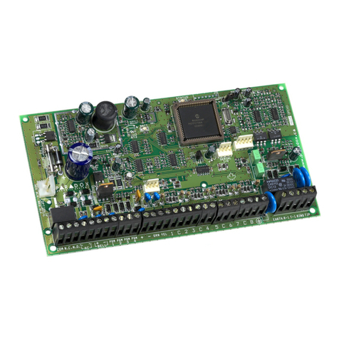
Introduction8
• Occupies one VME slot
1.3 Front Panel
The following figure shows the front panel of the ES1391.1 Power Supply
Controller Board
.
Fig. 1-2 Front Panel of the ES1391.1 Power Supply Controller Board
ES1391.1
PwrCtrl0
SwCtrl1
SwCtrl0
PwrCtrl1

Introduction 9
1.4 Block Diagram
Fig. 1-3 shows the block diagram of the ES1391.1 Power Supply Controller
Board.
The individual functions and interfaces of the board are described below.
Fig. 1-3 Block Diagram of the ES1391.1 Power Supply Controller Board
Overvoltage and Short Protection
All inputs/outputs of the top two power supply control units have both
overvoltage and short protection. All inputs/outputs (digital and analog) are
galvanically isolated.
All inputs/outputs of the bottom two switch control units also have both
overvoltage and short protection. The only exception is the programming port
for the EEPROM of the ES1392.1.
D/A and A/D Converters
A D/A converter with 14-bit resolution is used to generate the analog output
signals. The A/D converter for converting the pending analog variables at the
interface has 16-bit resolution. For details of the technical data, refer to
"Analog Inputs" on page 14 and "Analog Outputs" on page 15.
Over-
voltage /
Short
Protection
Processor
VMEbus Interface
16
Data
Flash
DAC Galvanic
Isolation
Over-
voltage /
Short
Protection
Over-
voltage /
Short
Protection
6
2
5
2
ADC
DAC
Over-
voltage /
Short
Protection ADC
Galvanic
Isolation
DIO
DIO
DOUT
DOUT
DIN
DIN

Introduction10
Motorola MPC555 Processor
The Motorola MPC555 is the processor used. It is responsible for signal
generation, measure variable processing and communication with the
VMEbus. It generates the digital and analog output signals and cyclically
acquires all digital and analog input signals. For details of the technical data,
refer to "Technical Data" on page 39.
VMEbus Interface
The ES1391.1 has a VMEbus slave interface. The base address can be set
dynamically by accessing the register or statically using hex switches.
For more information and addressing possibilities, refer to "Addressing the
ES1391.1 at the VMEbus" on page 23.
Data Flash
The Data Flash contains versioning information of the ES1391.1 and the
calibration data of the analog and digital inputs/outputs.

Hardware 11
2 Hardware
This chapter contains the descriptions of the hardware of the ES1391.1 Power
Supply Controller Board. It consists of the following sections:
• "Power Supply Control Unit" on page 12, description of the inputs/outputs
with technical data
– "Digital Inputs" on page 12
– "Digital Outputs" on page 13
– "Analog Inputs" on page 14
– "Analog Outputs" on page 15
• "Switch Control Unit" on page 17
– "Functions of the Switch Control Unit" on page 17
– "Control Output for Battery Nodes 0…4" on page 17
– "Alarm Input for Error Monitoring" on page 18
– "+UBatt and -UBatt Contacts" on page 19
– "Configuration Output for Battery Node 0" on page 19
– "Main Relay Input (MRC)" on page 20
– "Programming Port for the EEPROM of the ES1392.1 High Current
Switch Board" on page 22
• "Main Relay Function" on page 20: main relay switching and functions
• "Addressing the ES1391.1 at the VMEbus" on page 23
• "Optional Piggybacks" on page 26

Hardware12
2.1 Power Supply Control Unit
The power supply control unit has a connector with 14 pins. The unit is used
for addressing and controlling an external power supply.
Digital outputs can be configured depending on the power supply used. They
can be used, for example, to power on/off the power supply or power on/off
the supply voltage of the power supply (e.g. with the ES4080, ES4081 from
Takasago). The digital inputs detect overvoltage or overheating of the power
supplies. Every analog and digital input/output is galvanically isolated.
2.1.1 Digital Inputs
Every digital input has a pull-up/pull-down circuit for power supplies whose
status lines have an ”open collector” at the output. This circuit is configured
using jumpers.
Block Diagram
Fig. 2-1 Block Diagram of the Digital Inputs
For more details on jumper configuration, refer to "Jumper c: Digital Input 0"
on page 30.
+5 V
(galv. isolated)
Jumper
Pull-Up/
Pull-Down
Resistor
Digital
Input
Digital Ground
(GND-PwrCtrl)
Input Protection Galvanic
Isolation
DigIn
GND
Processor
MCP555
Digital Ground
(GND-PwrCtrl)

Hardware 13
Technical Data of the Digital Inputs
Tab . 2 - 1 Technical Data of the Digital Inputs
2.1.2 Digital Outputs
The digital outputs of a power supply control unit can be realized either as
simple switching contacts (open collector output) or can be assigned a pull-up
to 5 V by setting a jumper (TTL output).
Short-circuit-proof PhotoMOS relays are used as switching contacts. Their turn-
on time is approx. 500 μs. Their turn-off time is approx. 80 μs.
The pull-up functionality is realized with constant current sources which
provide an output current of 10 mA.
The delay times of the switching contacts are small in comparison to the typical
response times of the addressed power supplies. These are over 100 ms when
setting voltage states; with high-current circuits the delay time is over 50 ms.
This means that the delay time can be ignored with digital outputs.
Input Variable Data
Input voltage TTL
Input current <5mA
Overvoltage protection Yes, to ±60 V
Galvanic isolation Yes
Sampling rate 1 ms

Hardware14
Block Diagram
Fig. 2-2 Block Diagram of the Digital Outputs
For more details on jumper configuration, refer to "Jumper a: Digital Output
0" on page 30 and "Jumper b: Digital Output 1" on page 30.
Technical Data of the Digital Outputs
Tab . 2 - 2 Technical Data of the Digital Outputs
2.1.3 Analog Inputs
Serial A/D converters are used to measure the analog signals of the power
supplies. The galvanic isolation takes place in the serial connection between
the A/D converter and the MPC555 processor.
Output Variable Data
Output voltage Open collector/TTL
Output current 10 mA
Overvoltage protection Yes, to ±60 V
Galvanic isolation Yes
Switching frequency Max. 500 Hz
PhotoMOS
Relay with
Overvoltage
Protection
0 ... 60 V
Processor
MPC555
+5 V
(galv. isolated)
Jumper for Pull-Up Resistor
Pull-Up
Resistor
Digital Output
Digital Ground
(GND-PwrCtrl)
DigOut
GND

Hardware 15
Block Diagram
Fig. 2-3 Block Diagram of the Analog Inputs
Technical Data of the Analog Inputs
Tab . 2 - 3 Technical Data of the Analog Inputs
2.1.4 Analog Outputs
Serial D/A converters are used to generate the analog control voltages for the
power supply. The galvanic isolation takes place in the serial connection
between the D/A converter and the MPC555 processor.
Block Diagram
Fig. 2-4 Block Diagram of the Analog Outputs
Input Variable Data
Input voltage 0 to 10 V
Input impedance >1 MΩ
Accuracy ±3 mV (10.7-bit) typical
Resolution 16-bit
Sampling rate 1 ms
Galvanic isolation Yes
Overvoltage protection Yes, to ±60 V
Analog
Input
Analog Ground
(common)
Overvoltage
Protection
A/D
Converter
Galvanic
Isolation
Processor
MPC555
Analog
Output
Analog Ground
(common)
Overvoltage
Protection
D/A
Converter
Galvanic
Isolation
Processor
MPC555

Hardware16
Technical Data of the Analog Outputs
Tab . 2 - 4 Technical Data of the Analog Outputs
Output Variable Data
Output voltage 0 to 10 V
Output current 10 mA
Resolution 14-bit
Accuracy ±2 mV (11.2-bit) typical
Galvanic isolation Yes
Overvoltage protection Yes, to ±60 V

Hardware 17
2.2 Switch Control Unit
The switch control unit has a connector with 14 pins. It provides control signals
for addressing the battery nodes (relays) of the ES1392.1 High Current Switch
Board. The pins also have other functions which are explained below.
2.2.1 Functions of the Switch Control Unit
• Control output for battery nodes 0…4
• Configuration output for battery node 0
• Alarm input for error monitoring
• Main relay control input (MRC = Main Relay Control)
• Programming port for the EEPROM of the ES1392.1)
2.2.2 Control Output for Battery Nodes 0…4
This output switches the relevant relay on the ES1392.1. H level activates the
relay, i.e. it is closed, L level deactivates the relay, i.e. it is opened. An open
output is brought down to L level on the ES1392.1 by pull-down. This means
that if an output is open, the battery node is deactivated.
Tab . 2 - 5 Control Signal and Switch Position when Addressing the Battery
Node
The following table shows the technical data of the control output for battery
node x
Tab . 2 - 6 Technical Data of the Control Output for Battery Node x
Control Signal Switch
L/open Open
HClosed
Control Output of Battery Node x Data
Output voltage TTL
Output current 10 mA
Galvanic isolation No
Overvoltage protection Yes, to ±60 V

Hardware18
2.2.3 Alarm Input for Error Monitoring
The ES1391.1 Power Supply Controller Board is informed of any errors, e.g.
overcurrent or overheating at the battery node, by the ES1392.1 High Current
Switch Board via the alarm input.
The user can define the reaction of the ES1391.1 firmware when an error
arises via the RTIO configuration software. The ES1391.1 can power off both,
one or none of the power supplies addressed by the ES1391.1 as a reaction to
an active alarm signal.
If an error is detected at one of the battery nodes on the ES1392.1 High
Current Switch Board, the ES1392.1 opens the relevant node. After a delay
time of max. 800 ms, the node is automatically opened again to check
whether the error has been recovered. The node is opened immediately when
an overcurrent reoccurs. This is repeated until no overcurrent occurs. This also
has an effect on the power supplies connected to the ES1391.1 Power Supply
Controller Board.
Tab . 2 - 7 Level at the Alarm Input during Normal Operation and an Error
The following table contains the technical data of the alarm input:
Tab . 2 - 8 Technical Data of the Alarm Input for Error Monitoring
note
The cyclical current pulses during an overcurrent can exceed the current
limitation of some power supplies. In this case, the battery voltage should be
buffered with a large capacitor at the output of the power supply or a low-
impedance power resistor should be inserted into the battery voltage line to limit
the current.
State Status Signal
Normal operation L
Error H
Alarm Input Data
Input voltage TTL
Input current <1 mA
Galvanic isolation No
Overvoltage protection Yes, to ±60 V

Hardware 19
2.2.4 +UBatt and -UBatt Contacts
These contacts carry the supply voltage for the pull-up and pull-down resistors
of the main relay input (MRC).
The following table contains the technical data of the +UBatt and –UBatt
contacts:
Tab . 2 - 9 Technical Data of the +UBatt and –UBatt Contacts
2.2.5 Configuration Output for Battery Node 0
Battery node 0 on the ES1392.1 High Current Switch Board can be switched
against the battery voltage +UBatt and also (alternatively) against the battery
ground –UBatt.
If high is pending at the configuration output, battery node 0 switches to
battery ground; if low is pending, the battery node switches to battery voltage.
Tab . 2 - 10 Response of Battery Node 0 Depending on the Level at the
Configuration Output
The following table contains the technical data:
Tab . 2 - 11 Technical Data of the Configuration Output for Battery Node 0
+UBatt/-UBatt Contact Data
Input voltage 0 to 60 V
Input current Max. 1 A
Galvanic isolation Yes
Overvoltage protection Yes, to 60 V
Level at the Configuration Output Response of Battery Node 0
L (Low) Switches to battery voltage
H (High) Switches to battery ground
Control Output of Battery Node x Data
Output voltage TTL
Output current 10 mA
Galvanic isolation No
Overvoltage protection Yes, to ±60 V

Hardware20
2.2.6 Main Relay Input (MRC)
Depending on the signal at the main relay input, the battery nodes can be
activated or deactivated. The user defines which battery nodes depend on the
main relay and whether the main relay signal is high-active or low-active via
the RTIO.
The following table contains the technical data of the main relay input:
Tab . 2 - 12 Technical Data of the Main Relay Input
Main Relay Function
The ES1391.1 makes it possible to evaluate an existing signal from the
connected ECU directly in the hardware for addressing a main relay
(MRC=Main Relay Control) and to include this in the activation/deactivation of
the individual battery nodes. The ECU signal is accepted by the ES1392.1 High
Current Switch Board and routed from this board to the main relay input of the
ES1391.1.
Depending on the state of the main relay signal, individual battery nodes can
be activated. The battery nodes dependent on the MRC signal are defined
using the RTIO configuration software.
The main relay input of the ES1391.1 Power Supply Controller Board can be
assigned a pull-up to battery voltage or a pull-down to battery ground.
A subsequent comparison with the half battery voltage returns logical level
information (high or low) which is supplied to the processor. The processor
then decides whether the signal is active or inactive based on the polarity set
by the user for the main relay signal (low-active or high-active) via the RTIO
configuration software. The processor closes or opens those battery nodes
which are controlled by the status of the main relay input in accordance with
this active/inactive information.
Main Relay Input Data
Input voltage 0 to 60 V
Input current 0-20 V: 100 mA, 20-40 V: 50 mA, 40-
60 V: 33 mA
Galvanic isolation Yes
Overvoltage protection Yes, to ±60 V
Table of contents
Other ETAS Controllers manuals