FSBB15CH60 Motion SPM® 3 Series
©2006 Fairchild Semiconductor Corporation 7www.fairchildsemi.com
FSBB15CH60 Rev. C6
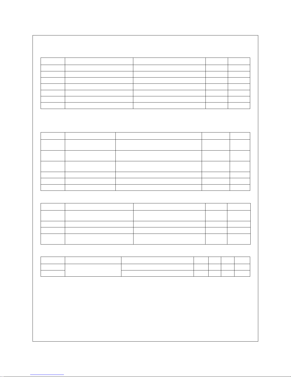
Electrical Characteristics (TJ= 25°C, unless otherwise specified.)
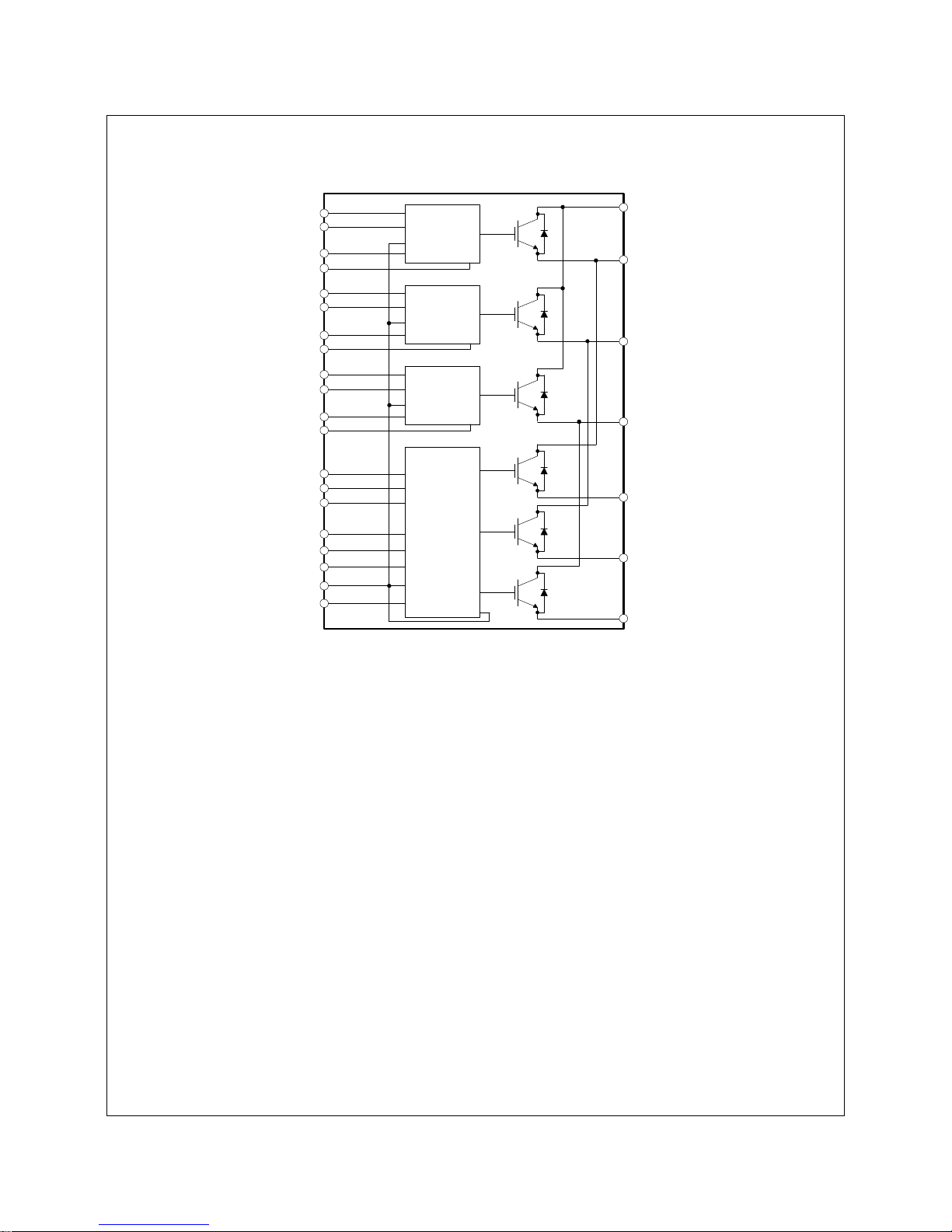
Control Part
2nd Notes:
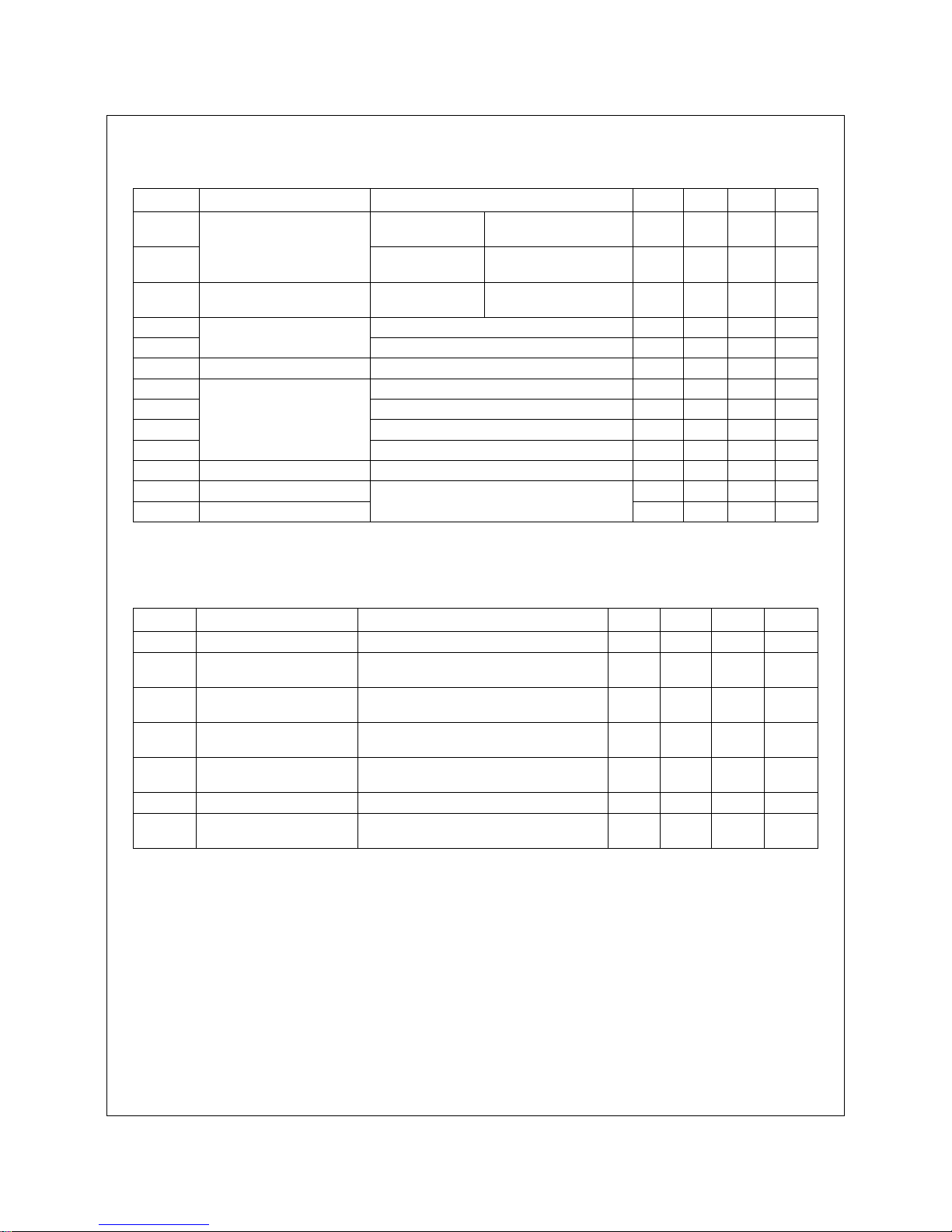
4. Short-circuit protection is functioning only at the low-sides.
5. The fault-out pulse width tFOD depends on the capacitance value of CFOD according to the following approximate equation: CFOD = 18.3 x 10⁻⁶ x tFOD [F]
Recommended Operating Conditions
Symbol Parameter Conditions Min. Typ. Max. Unit
IQCCL Quiescent VCC Supply
Current VCC = 15 V
IN(UL, VL, WL) = 0 V VCC(L) - COM - - 23 mA
IQCCH VCC = 15 V
IN(UH, VH, WH) = 0 V VCC(UH), VCC(VH), VCC(WH)
- COM - - 100 A
IQBS Quiescent VBS Supply Current VBS = 15 V
IN(UH, VH, WH) = 0 V VB(U) - VS(U), VB(V) - VS(V),
VB(W) - VS(W)
- - 500 A
VFOH Fault Output Voltage VSC = 0 V, VFO Circuit: 4.7 kto 5 V Pull-up 4.5 - - V
VFOL VSC = 1 V, VFO Circuit: 4.7 kto 5 V Pull-up - - 0.8 V
VSC(ref) Short Circuit Current Trip Level VCC = 15 V (2nd Note 4) 0.45 0.50 0.55 V
UVCCD Supply Circuit Under-Voltage
Protection Detection Level 10.7 11.9 13.0 V
UVCCR Reset Level 11.2 12.4 13.2 V
UVBSD Detection Level 10.1 11.3 12.5 V
UVBSR Reset Level 10.5 11.7 12.9 V
tFOD Fault-out Pulse Width CFOD = 33 nF (2nd Note 5) 1.0 1.8 - ms
VIN(ON) ON Threshold Voltage Applied between IN(UH), IN(VH), IN(WH), IN(UL),
IN(VL), IN(WL) - COM 3.0 - - V
VIN(OFF) OFF Threshold Voltage - - 0.8 V
Symbol Parameter Conditions Min. Typ. Max. Unit
VPN Supply Voltage Applied between P - NU, NV, NW- 300 400 V
VCC Control Supply Voltage Applied between VCC(UH), VCC(VH), VCC(WH),
VCC(L) - COM 13.5 15 16.5 V
VBS High-Side Bias Voltage Applied between VB(U) - VS(U), VB(V) - VS(V),
VB(W) - VS(W)
13.0 15 18.5 V
dVCC / dt,
dVBS / dt Control Supply Variation -1 - 1 V / s
tdead Blanking Time for Preventing
Arm-Short For Each Input Signal 2.0 - - s
fPWM PWM Input Signal -20C TC100°C, -20C TJ125°C - - 20 kHz
VSEN Voltage for Current Sensing Applied between NU, NV, NW - COM
(Including Surge Voltage) -4 4 V