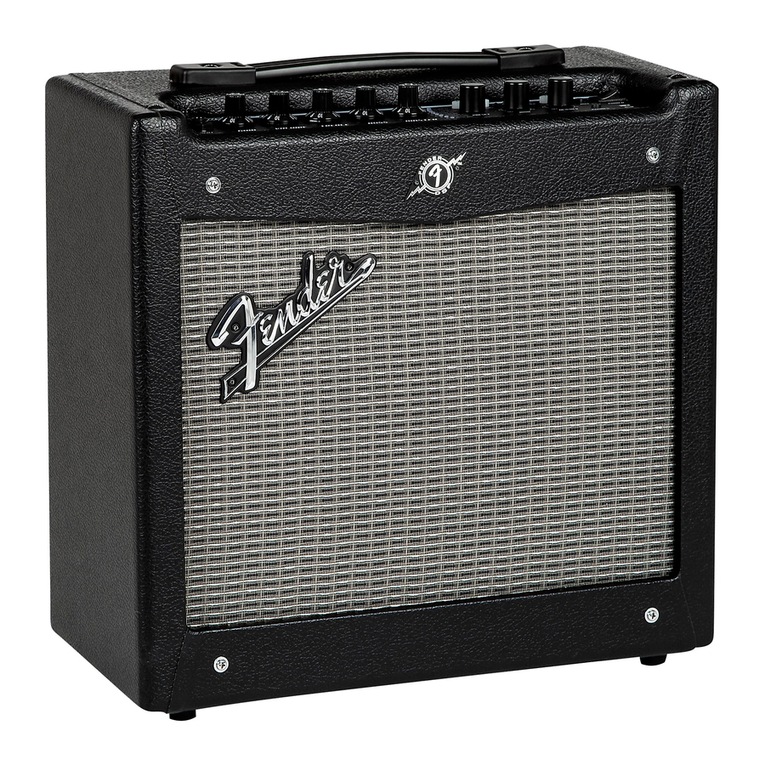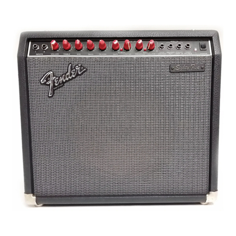
SUPER CHAMP®XD
(This is the model name for warranty claims)
5
PCB EXCHANGE POLICY
Parts marked with a single asterisk (*) in the Part
Lists are not field replaceable. If a failure due to
one of these components is detected, please con-
tact the FMIC Customer Service Department to
order the complete PCB Assembly.
CIRCUIT DESCRIPTION
This section provides concise information about new
or unusual circuitry designs incorporated into this
amplifier model. The purpose is to aid the service
technician by providing insight into the design areas
most likely to become obstacles in troubleshooting.
Information is focused for its effective use while
maintaining the security of Fender® proprietary in-
formation wherever possible.
MAIN PCB
The main PCB contains the circuitry for the pre-
amplifier, the power amplifier and the power supply.
The controls are located on a breakaway section of
the main PCB with ribbon cables connecting them.
PRE-AMPLIFIER
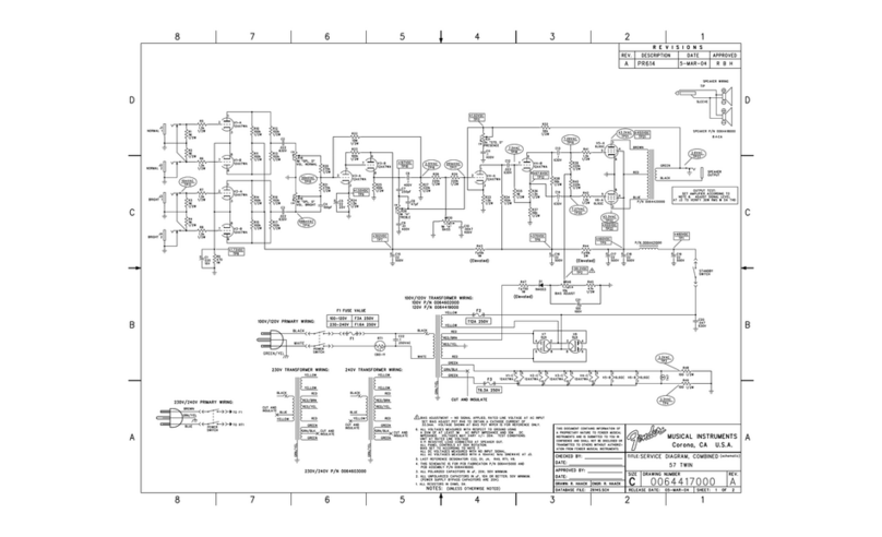
Op-amp U7-A provides the high impedance instru-
ment input with 15db of gain. Op-amp U7-B is
configured as a three pole active filter. The filtered
output signal (Lin) drives the encoder portion of the
CODEC U13 of the uDSP PCB. Signal VQ2 is the
D.C. reference voltage from the CODEC thus center-
ing the output signal about this level. Op-amp U3-A
is configured as a differential input amp recovering
the signal after uDSP processing and conversion
back to an analog signal in the decoder portion of the
CODEC U13. The LOUT+ and LOUT- signals are the
input to the differential amp which acts as a three
pole active low pass filter. The output of U3-A is ap-
plied to a buffer amp U1-A which drives op-amp U1-
B which provides the LINE OUT signal and the
power amp input. FET Q1 provides system muting
during power up/down in conjunction with the power
sense circuits comprised of D9, Q2 and Q4.
USER INTERFACE
The 4 - 16 position encoders (S2 –S3) for the VOICE
and EFFECT SELECT are read via the port ex-
pander U4 and the data sent to the uDSP system via
the I
2
C interface lines SCL and SDA.
The 6 potentiometers CH1 VOLUME (R85), CH2
VOLUME (R83), CH2 GAIN (R84), TREBLE (R82),
BASS (R81) and FX LEVEL (R80) generate DC volt-
ages (+1.0V to +4.0V) that are read by the analog
multiplexer U6. IO0-IO3 are the digital control lines
used to multiplex these analog signals which are
sent serially to the system CODEC U13 on the Rin
channel. The uDSP system reads the state of these
controls and inputs digitally from the CODEC.
POWER AMPLIFIER
The power amplifier consists of V1, V2, V3, T2 and
associated circuitry. The signal is fed to the gate of
V1-B in common cathode configuration. The signal
is then fed from the plate of V1-B to the gate of V1-
A which is operating as a phase splitter which
drives V2 from its plate and V3 from its cathode. V2
and V3 are operating in class A-B push-pull mode.
T2 matches the impedance of V2’s plate to the 8
Ohm speaker. Negative feedback is provided by
R23 feeding signal back to V1-B’s cathode.
uDSP PCB
The uDSP PCB is located in the back of the chassis
opposite the power transformer. It provides the am-
plifier voicing and effects functions. The uDSP PCB
is not field serviceable and must be replaced as an
assembly.
