FETAudio FDA-2A User manual
FDA-2A Manual.doc Rev. 1.0
Page 1 31-Aug-2012
www.FETAudio.com
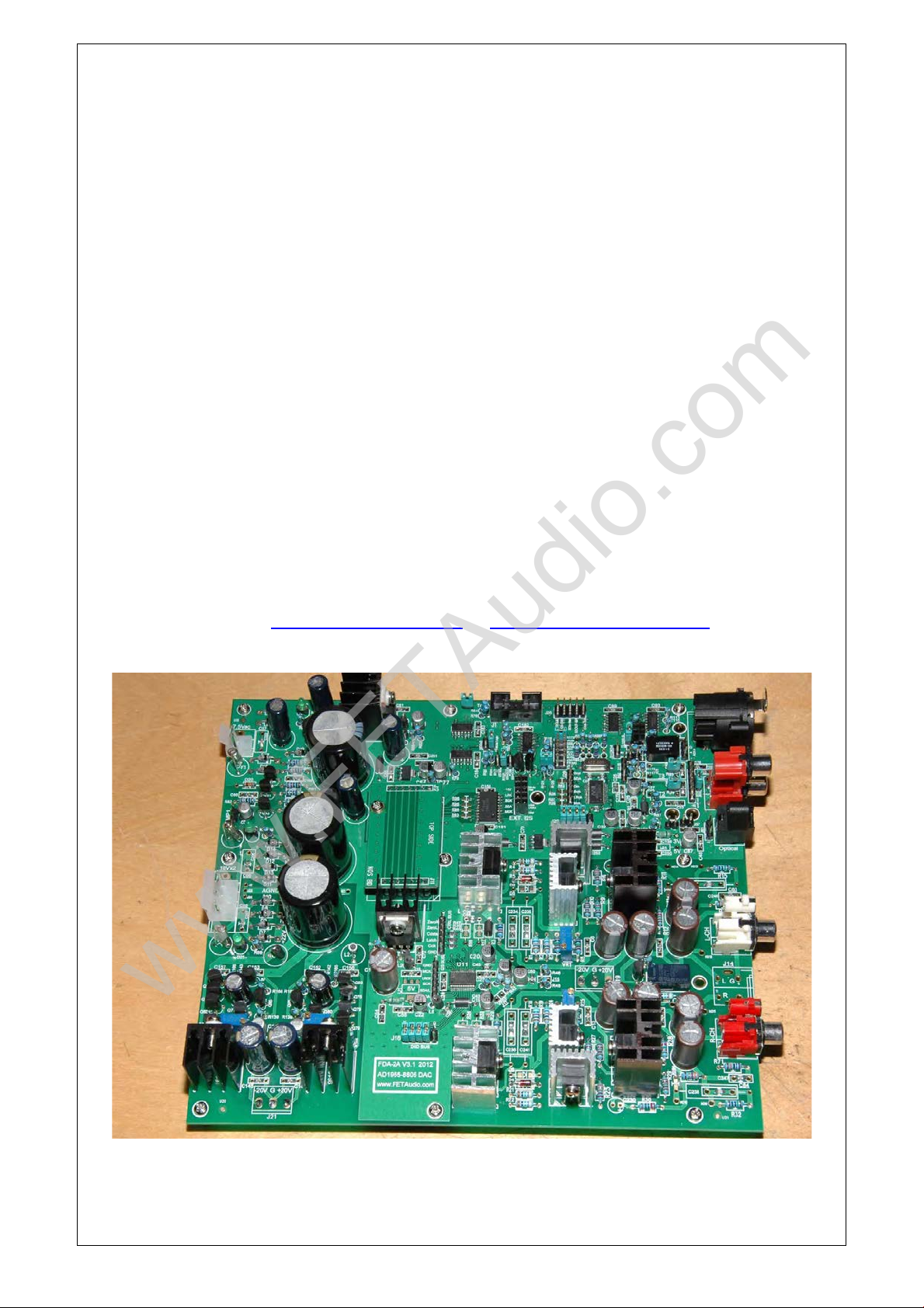
FDA-2A Manual
AD1955 + WM8805 Single Ended DAC
~~~~~~~~~~~~~~~~~~~~~~~~~~~~~~~~~~~~~~~~
High Fidelity 24 bit*192kS/s
Digital to Analogue Converter
~~~~~~~~~~~~~~~~~~~~~~~~~~~~~~~~~~~~~~~~
Designed By Spencer Cheung of FETAudio.com
Email: spencer@fetaudio.com or skcheung68@hotmail.com
www.FETAudio.com
FDA-2A Manual.doc Rev. 1.0
Page 2 31-Aug-2012
A. Introduction:
FDA-2A AD1955+WM8805 DAC use the same “super sound discrete IV converter” of FDA-1B.
The main difference is the change of the main DAC chip from Texas Instruments PCM1794A
to Analogy Devices AD1955 in Single Ended output mode.The second minor change is the
digital receiver chip from WM8804 to WM8805. Due to the use of AD1955 DAC chip in FDA-
2A, it sounds smoother, more laid back, and less dynamics relative to FDA-1B PCM1794A
DAC. In fact many people like this type of sound and regard it as more musical. This
reminds me the sound of PCM63 in D1V33 DAC. Overall, FDA-2A DAC sounds more like the
mixture of D1V33 and FDA-1B with the 24bit high resolution.
So who is the winner? To me it is a matter of taste for the choice of DAC chip to match with
the rest of Hi-Fi system. Personally I think FDA-1B PCM1794A DAC is a better match to valve
amplifiers and FDA-2A AD1955 DAC suit more on solid states amplifiers.
In FDA-2A, the AD1955 DAC chip will work in its reset default mode, i.e. PCM mode. Thus
FDA-2A natively is able to work up to 24bit/96k with “NOS Daughter Board” due to the
limitation of AD1955 default PCM mode. To let it play 24bit/192k input signal, an “ASRC
Daughter Board” is required (same board used in the FDA-1B) to down sample 192k digital
signal back to 96k for the AD1955 chip to decode.
On the WM8805 receiver side, it is preset to hardware mode but input logics allow it to
have 4 digital inputs (2 SPDIF, 1 AES and 1 Toslink) and one I2S input with a new front panel
control board.The FDA-1B front control board is also usable but it only can control 3x
digital input plus 1x I2S or 4x digital input without I2S input.Moreover one of the two RCA
socket (top one) on digital input section can be set to SPDIF out of WM8805 by on board
jumpers. It functions as a buffer and jitter filter/cleaner of the selected digital input signal
(not for I2S input).
Since this is a DIY DAC, it will work as a standalone DAC. But there are “control bus” sockets
delicate to control both the AD1955 and WM8805 chips on board in software mode. This is
made for DIYer to improve the DAC further for functionality and user interface. If the DIYer
knows SPI & MCU software program, the DAC can be transformed into full software mode
to extend the full functions of the DAC without sacrificing performance of sound. Some
possible additional functions are 24bit/192k native support, DSD direct input support, , 4
more digital inputs (total 8), testing of mono mode, external digital filter mode via new
module at U18 daughter board, adding display to show sample rate and working status of
the DAC, slaving the internal DAC system clock to external low jitter Super Clock reference,
adding a USB2.0 to I2S module via I2S input at J5 etc…
Thus this DAC design is really flexible for user to experiment with different modes of the
AD1955 and WM8805 chips!The price is just a faction of the demo board of Wolfson or
Analogy Devices and it has two chips on one single board.With the super sound discrete
IV converter, it is able to explore the best sound from these chips available for PCM and
DSD format.
www.FETAudio.com
FDA-2A Manual.doc Rev. 1.0
Page 3 31-Aug-2012
B. Specifications:
1. DAC chip AD1955 and receiver chip WM8805 plus the discrete super sound IV
converter in pure class “A” operation.
2. On board full power supplier regulations for the DAC to work in standalone
hardware mode with 4 digital inputs (2 SPDIF – RCA x 2, 1 AES – XLR x 1, & 1
Optical – Toslink x 1) and one I2S (2x5 2.54mm pin header) input. Moreover one of
the RCA SPDIF input socket can be set to SPDIF out, but by doing so, number of RCA
SPDIF input will be one only.
3. Control buses for AD1955 and WM8805 chips are provided on board and thus it can
program into software mode and expand the functions of the DAC.
4. Accept up to 24bit/96k signal in NOS mode or 24bit/192k signal with ASRC Daughter
Board (Use same Daughter Board options of FDA-1B).
5. Output analogy level at about 1.5Vrms at 0dBFS digital input. Distortion is about
0.02% at 1kHz 0dbFS or below 0.04% from 20Hz-20kHz.Output impedance is about
150 ohm. Output mute is provided with relay shorting the signal to ground.
6. Power supply is AC 18V x 2 and 9V x 1 (same as FDA-1B transformer); min 40VA total.
7. The form factor of the PCB is similar to the FDA-1B with one discrete IV section and
one regulator removed. Since the PCB width is only 7.1 inches, it will fit into a half
full size case of about 9 inches width.
8. Board: 7.1 x 8 inches double sided 1.6mm gold plated FR4; 9 x M3 supporting holes;
max height part 35mm. Total fully assembled board height is 37mm.
9. The PCB layout is designed to accept both SMD and Through-Hole type components
for both capacitors and resistors. Note that although the resistors hole is just a TH
5mm pitch but 0805 SMD parts can be soldered on to it.
10. Future expansion to USB 2.0 (up to 24bit/192k) input using any USB to I2S module
solution is possible via the input daughter board using the I2S digital input at J5.
Component Choices:
1. Best DAC chip AD1955 and best sound receiver WM8805 are used.
2. All logic parts are selected carefully to ensure digital input can work flawlessly up to
192k sample frequency.
3. Many Toshiba obsolete transistors are eliminated and better parts are selected from
various sources to ensure continue supply. Many Fairchild transistors are used for
the better specifications and easily available from Mouser or Digikey.
4. Vishay MRS25 and Xicon 50ppm 1% resistors are widely used.
5. Maintain the use of Elna Silmic II capacitors in the analogy discrete IV sections for its
best sonic performance.
6. Use more SMT capacitors (both E-cap and MLCC) in the digital section as they are
more stable with lower ESR.Example is Panasonic FK series. The 5600p and 1500p
IV low pass filter capacitors have changed to SMT COG type for more accurate and
stable performance.
7. ROHS compliance is the first choice for all components.
www.FETAudio.com

FDA-2A Manual.doc Rev. 1.0
Page 4 31-Aug-2012
C. Assembly Instruction
1. Please take necessary ESD precautions, as all the parts are ESD sensitive!
2. Solder all SMD IC: AD1955, WM8805, 74 Series ICs, and AMS1117,Align the markings of
the parts with the text on the PCB screen-printing.
3. Solder all SMD chip capacitors (0603 or 0805 sizes) provided as per below sequence.
They are 15pF x 2, 100p x 2, 470p x 2, 1u x 1, 1500p x 2, 5600p x 4, 0.01u x 2, 0.1u x 58.
4. Solder the SMT crystal 12MHz Y1 on board.
5. After that wash the PCB to remove all the flux with Isopropyl Alcohol. Use a tooth brush
to clean the gap of the ICs leads. After that rinse the PCB with distilled water and dry it
properly.
6. Use a multi meter to check all the leads of AD1955 and WM8805 connections to the
nearest connection points. Ensure no adjacent leads are shorted together unless it is
designed to be shorted.
*** If you buy the kit, you will get a DAC main board with all the SMT parts pre-
soldered as above ***
www.FETAudio.com
FDA-2A Manual.doc Rev. 1.0
Page 5 31-Aug-2012
7. Solder the rest of the parts starting from the smallest parts first, preferably also by
component type and by component value. For example, beads (except L8 and L15), Pin
Headers, pulse transformer, relays, resistors, LEDs, diodes, small E-caps and TO-92
transistors, VRs, Connectors, fuses etc… Leave the big items like E-caps 10000u, 5600u,
560u, 470u, and 100u silmic, RCA/XLR sockets to be soldered at the end of the process.
8. For SMD E-capacitors (Panasonic FK and other 5mm type if provided), pull the leads
straight carefully and insert into the PCB holes before soldering. Do not pull the lead too
hard as it may break. Note there is polarity for these E-caps (negative at black strip or
semi-circle).
9. Do not solder L8 and L15 nearby the AD1955 chip. This is only required after checking
the regulator voltage is regulating at 5Vdc in the tuning procedure.
10. There are some parts that need special attentions during assembly:
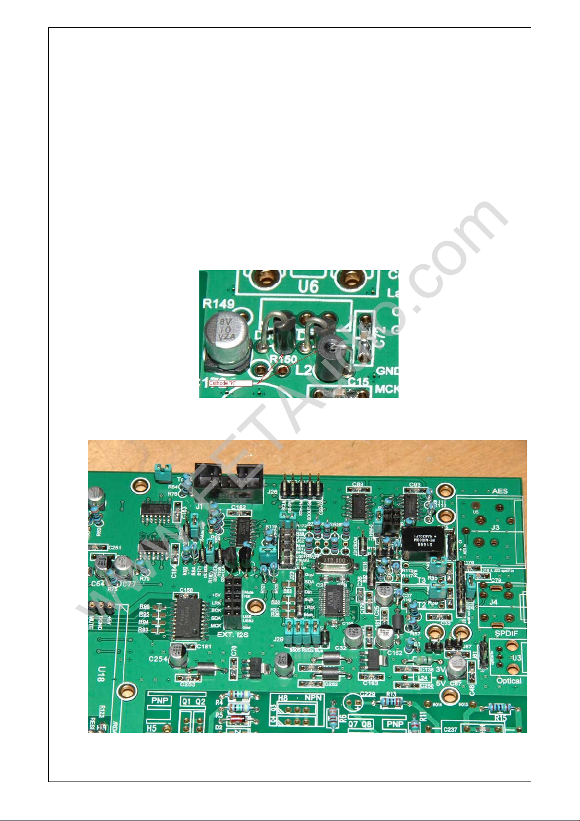
10.1. Diodes 1N4007 x 4 pcs – D34 to D37: The cathode mark (strip or K) is not
provided on the PCB, it is actually the double circles on the PCB.
10.2. Pin Headers for both male and female type – refer to photo below for the
type of pin header or socket.Some pin headers will require a jumper inserted after
soldering as shown.
www.FETAudio.com
FDA-2A Manual.doc Rev. 1.0
Page 6 31-Aug-2012
10.3. Do not connect the 3 wires at J19 and J21. Refer to the tuning procedure for
details.
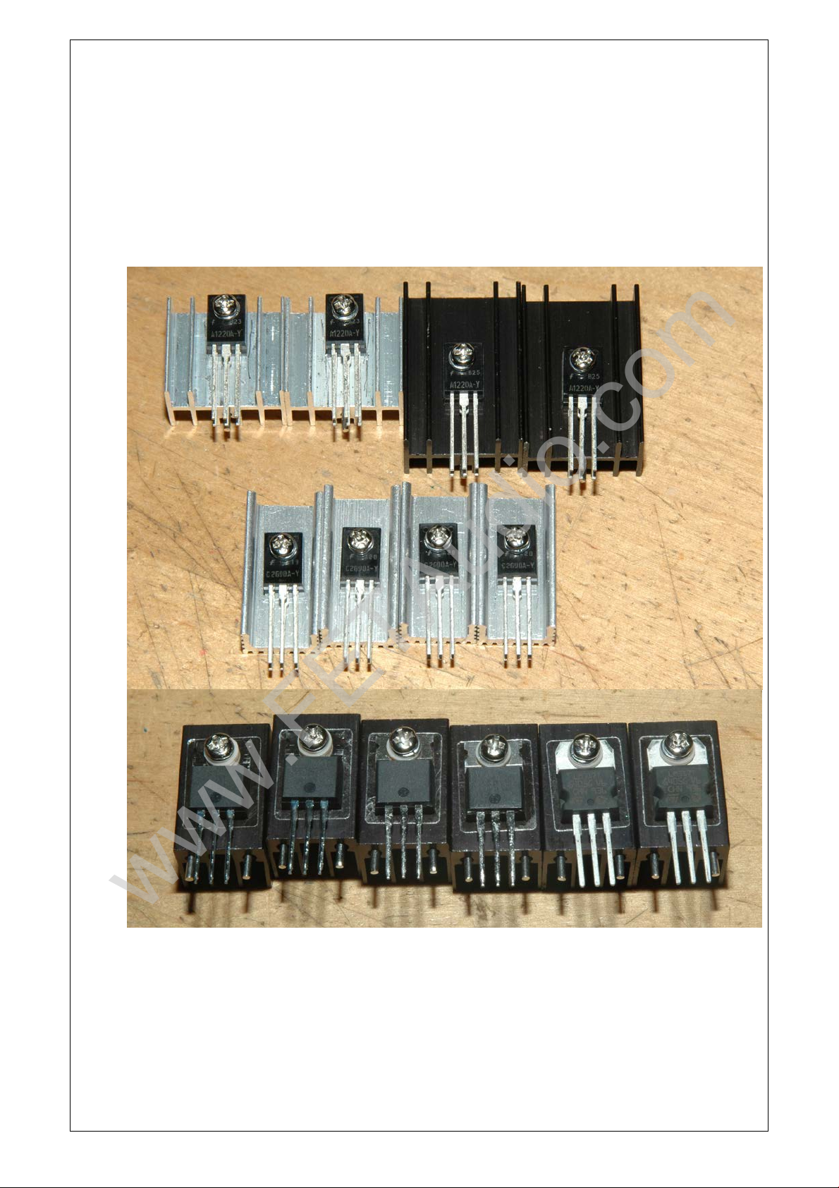
10.4. Install all transistors into heat-sink with their markings all facing upward as
shown below. Note that there is a mica insulation sheet between the metal body of
TO-220 parts (IRF610, IRF9610 and LM317T) and the heat sink.A spring washer and
plastic washer is also used for insulating the M3 screw from touching the metal
body of all TO-220 parts. For the other NPN and PNP transistors, they do not need a
mica sheet for insulation as the body is all 100% plastic.
www.FETAudio.com
FDA-2A Manual.doc Rev. 1.0
Page 7 31-Aug-2012
10.5. If ASRC daughter board module is used, the output sample frequency Fs can
be set as below:
ASRC Chip
J15
J16
Sample Frequency
SRC4192
Open
Open
96k (recommended)
SRC4192
Open
Short
48k
SRC4192
Short
Open
192k (No Output)
SRC4192
Short
Short
No Output
AD1896
Open
Open
96k (recommended)
AD1896
Open
Short
48k
AD1896
Short
Open
32k
AD1896
Short
Short
No Output
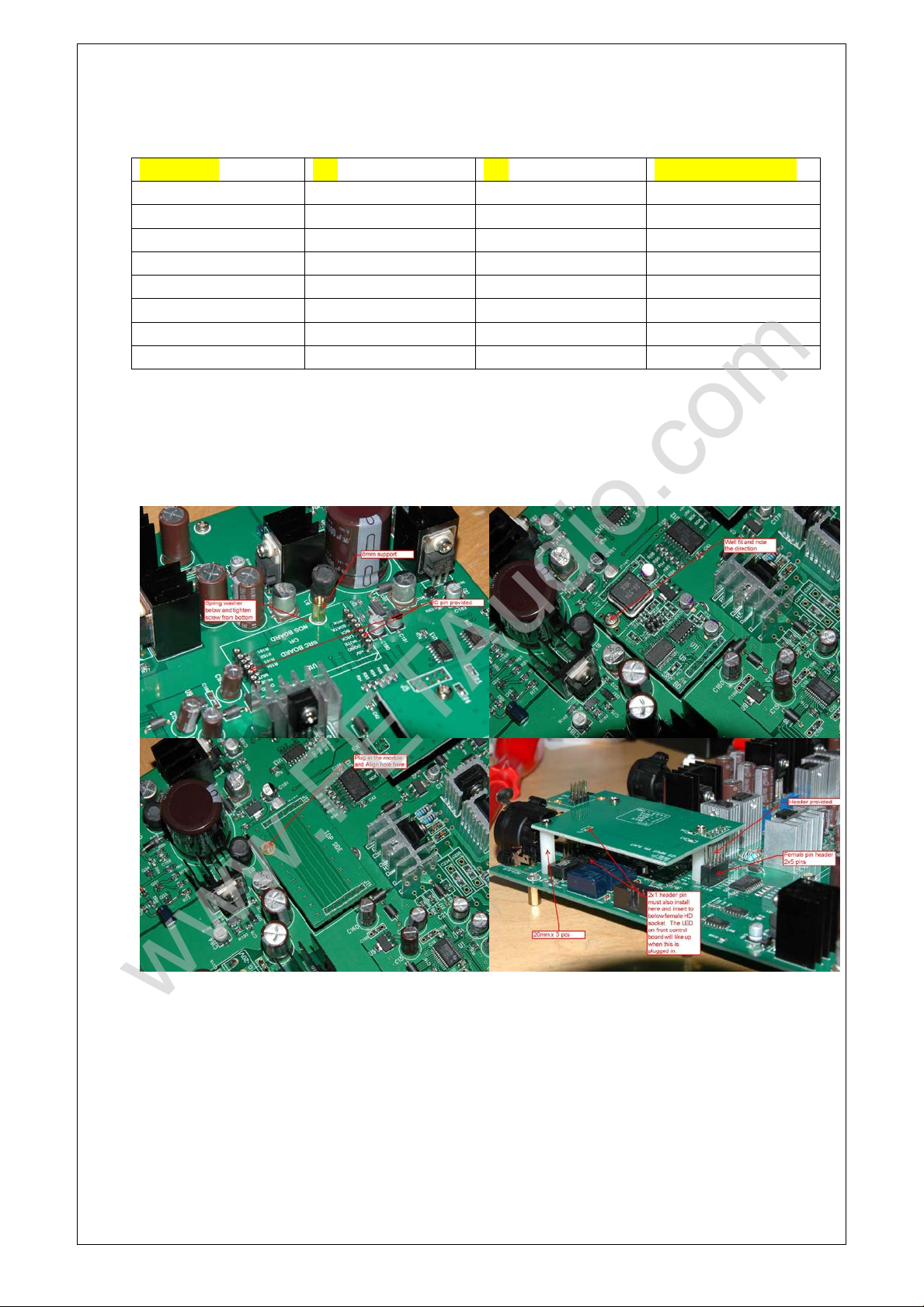
Note the orientation of the ASRC daughter board and it must be inserted like the photo
below. The fixing screw should be able to be aligned to the spacer hole. The M3 spacer
provided is 8mm height and a spring washer is provided and put below the spacer to
increase the total height to about 9mm. Two rows of IC pin sockets are provided and to
be soldered on the main board. NOS or ASRC and RJ45 daughter boards should be
inserted into the main board as shown.
Photo above is for reference only as the main board may be a difference version.
www.FETAudio.com

FDA-2A Manual.doc Rev. 1.0
Page 8 31-Aug-2012
D. Tuning and Testing Procedures:
1. With all the parts in place except the 3 wires, L8 and L15, insert the NOS daughter board
in place (U18).
2. Connect AC 9V (or a regulated power supply with current limit set to 200mA at 12Vdc)
to J55 (do not connect J58 and J59 to AC 18V), check the voltages at U1 big pad (5V), U6
and U7 (LM317T) metal body (not the big heat-sink that it attached to) relative to
ground (DGND at U18 daughter board). The voltage at all 3 locations should be at about
5V +/- 0.1Vdc. If the voltage is outside the range, cut off the power immediately and
check for wrong component used or open/short soldering.
3. Solder L8 and L15 if the regulated voltage at U1 and U6 are at 5V.
4. Then check the voltage at U8, U10, & U17 (AMS1117-3.3). The voltage at the little heat-
sink of the regulators should be 3.3V +/- 0.1Vdc.
5. Plug in the Front Panel Control Board (V7.1) via J1 on both PCBs using the 10-pin flex
cable provided. D1 (USB/I2S) and D5 (if set to Power LED) should be “ON”. Press the
toggle switch (at J2 or J14) to see if the LEDs D1 to D4 is “ON” one by one.The sequence
is from D1 D4 D3 D2 D1 D4 … and repeat.
6. Inject a digital SPDIF1 signal to J4 (lower RCA socket), the LOCK LED (D6) should be “ON”
if SPDIF (D4) is selected. This shows that the digital section is locking to input signals.
7. Then remove the power at J55.
8. Connect AC18V (or a regulated power supply with current limit set to 300mA at 24Vdc)
to J59, check for voltage at J21 for -20V to G points. The initial voltage should be around
-15.5V to -16V. Adjust VR8 until the voltage is -20V +/- 0.02Vdc. Remove the power
applied to J59.
9. Connect AC18V (or a regulated power supply with current limit set to 300mA at 24Vdc)
to J58, check at J21 for +20V to G points. The initial voltage should be around 15.5V to
16V. Adjust VR7 until the voltage is +20V +/- 0.02Vdc. Remove the power applied to J58.
10. Solder the 3 wires provided from J19 to J21 at the bottom of PCB.Make sure that the
wires are connected from -20V to -20V, G to G and +20V to +20V points.
11. Connect power to all J55, J59 and J58.
Check the +20V and -20V are still at about the same voltages as before. If not, the IV
section is not work properly.Cut the power immediately and do trouble shooting. The
common mistake is transistor orientation wrongly mounted on the heat-sink.
12. Output DC offset adjustment:
13. Check the offset voltage at C246 (C83) inner hole relative to Ground (G point of J14). It
should be around -0.45Vdc. Adjust VR1 until this voltage to below +/-1mVdc. Repeat at
C247 (C84) and adjust VR2 to within +/-1mVdc offset.
14. After warm up for 30 minutes, repeat above steps 11 to 13 to ensure the offset is below
1mV by adjustment again if necessary. For normal use, the offset of +/-5mV is ok as all
output has couple capacitor to block any DC from going to the output sockets.
15. Re-adjust +20V and -20V regulated voltages if necessary
16. Check the DAC AD1955 analogy pins DC offset voltage at two sides of C56 and C67
(100pf SMD capacitors). The DC voltage relative to DGND should be at about 2.7xV
(close to 2.8V).
17. Check the VREF voltage of AD1955 at the J17 “Square” pad. The voltage should be close
to 2.39Vdc.
18. If all the DC adjustments and check are done, proceed to AC measurements below.
www.FETAudio.com

FDA-2A Manual.doc Rev. 1.0
Page 9 31-Aug-2012
19. Connect a 1kHz digital signal to the SPDIF1 input (lower RCA socket). A test CD recorded
with 1kHz can be used with a CD player with SPDIF output.
20. Check the output levels for 0dBFS input signal is about 1.55Vrms at J14 T1 and T2
relative to G. Left and right channel should not be more than 0.25dB differences in
levels.
21. Check that the distortion of the output 1KHz signal is about 0.022% for both channels.
22. Burn-in the DAC for an hour and go for listen test.
www.FETAudio.com

FDA-2A Manual.doc Rev. 1.0
Page 10 31-Aug-2012
E. Board Interface Specifications:
1. Power Supply Connectors:
Location
Description
Format
J58
18V to 20V AC, 0.8A, 14VA
3.96mm pitch (5mm also provided)
J59
18V to 20V AC, 0.8A, 14VA
3.96mm pitch (5mm also provided)
J55
8 to 9V AC, 1.2A, 12VA
3.96mm pitch (5mm also provided)
J2/J25/J54
Chassis Ground
Connect AGND to star ground point
2. External I2S Connector J5: (5 x 2 female Pin Header; pitch 2.54mm, CMOS 3V3 logic)
Pin
Description
Marking on PCB
1
Digital Ground
GND
2
System clock 256fs
MCLK
3
USB2 LED drive (with current limit R120)
USB2
4
Serial Digital Data
SDA
5
USB LED drive (with current limit R121)
USB
6
Bit clock 64fs
BCK
7
Power up reset (Low = Reset)
RST
8
Work clock fs
LRK
9
Output Mute (Hi = Mute)
Mute
10
+5V DC Supply for plugin
+5V
3. Digital Input Socket:
Location
Description
Spec
Format
J4
SPDIF input x 2 – Lower RCA is
SPDIF1; Upper RCA is SPDIF2 or
SPDIF Out (Tx from WM8805)
75 ohm 24bit/192k
RCA (vertical
double deck)
J3
AES input
110 ohm 24bit/192k
XLR female
U3
Optical input
Optical 24bit/192k
Toslink - TORX147
J5
See item 2 above
3.3V CMOS levels
5x2 pin header
Note: For 192k operation, an ASRC daughter must be used at U18 location.
4. Analogy Output Socket:
Location
Description
Format
J6
Left Single Ended Output
RCA (white)
J14
Left and Right output for wire connection
RCA (vertical double deck)
not provided
J7
Right Single Ended Output
RCA (red)
5. J1 – Front Panel connector (for hardware mode only):
Pin
Description
Marking on PCB
1
Digital input select Binary bit 0 (0, 0, A)
Default A = 1
2
Digital input select Binary bit 1 (0, B, 0)
Default B = 1
3
Digital input select Binary bit 2 (C, 0, 0)
Default C = 0
4
USB2 LED drive from pin 1 of J62 (no current limit) AND
pin 3 of J5 (with resistor R120=680R current limit).
USB2
www.FETAudio.com
FDA-2A Manual.doc Rev. 1.0
Page 11 31-Aug-2012
5
DGND
6
USB LED drive from pin 1 of J24 (no current limit) AND pin
5 of J5 (with resistor R121=680R current limit).
USB
7
+3V3 Supply from U8
8
Lock LED drive (with resistor 680R current limit)
Lock = Un-mute
9
+3V3 Supply from U8
10
Mute LED drive (with resistor 680R current limit)
Mute = un-lock
Default of digital input is set to (C,B,A=0,1,1), SPDIF1.
6. J26 – WM8805 Control Bus:
Pin
Description
Marking on PCB
1
DGND
2
CSB/GPO2
CSB-G2
3
DGND
4
SDOUT/GOP7
SDOUT-G7
5
DGND
6
SDIN/HWMODE
SDIn-Hw
7
DGND
8
GPO0/SWIFMODE
G0-SW
9
DGND
10
SCLK
SCLK
Refer to WM8805 data sheet for details
7. J20 – WM8805 Digital Bus:
Pin
Description
Marking on PCB
1
DGND
GND
2
DOUT
SDA
3
DIN
Din
4
BCLK
Bclk
5
LRCLK
LRck
6
MCLK
Mck
Refer to WM8805 data sheet for details
8. J29 – WM8805 RxGx Bus:
Pin
Description
Marking on PCB
1
GPO1
G1
2
DGND
3
RX4/GPO3
R4G3
4
DGND
5
RX5/GOP4
R5G4
6
DGND
7
RX6/GOP5
R6G5
8
DGND
9
RX7/GOP6
R7G6
10
DGND
Refer to WM8805 data sheet for details
www.FETAudio.com

FDA-2A Manual.doc Rev. 1.0
Page 12 31-Aug-2012
9. J12 – AD1955 Control Bus (SPI):
Pin
Description
Marking on PCB
1
DGND
GND
2
CCLK
Cclk
3
CLATCH-BAR
Latch
4
CDATA
Cdata
5
ZEROL
ZeroL
6
ZEROR
ZeroR
Refer to AD1955 data sheet for details
10. J13 – AD1955 Digital Bus (I2S):
Pin
Description
Marking on PCB
1
DGND
GND
2
MCLK
MCK
3
LRCLK
LRCK
4
BCLK
BCK
5
SDATA/L
SDA/L
6
/RDATA
/RDA
Refer to AD1955 data sheet for details
11. J16 – AD1955 DSD Bus:
Pin
Description
Marking on PCB
1
DGND
GND
2
DGND
3
DSD_PHASE
PHA
4
DGND
5
DSD_RDATA
RDA
6
DGND
7
DSD_LDATA
LDA
8
DGND
9
DSD_SCLK
SCLK
10
DGND
If DSD input is not used, short the all the pins to ground. Refer to AD1955 data sheet for
details
www.FETAudio.com

FDA-2A Manual.doc Rev. 1.0
Page 13 31-Aug-2012
12. JUMPERS, RESISTOR AND PIN HEADER DESCRIPTION:
Location
Description
R53/R88
Short one of these resistors; R88 = I2S Mute at J5 pin 9 is active High;
R53 = I2S Mute is active LOW. Default is R88 short (active high).
R171
If shorted, then the I2S Mute pin 9 is shorted to ground, thus the Mute
conditions will depend on the setting of R53 and R88. Default is R171
open.
R107/R106
Short one of these resistors; If R107 is shorted, I2S input will be selected
at (A,B,C)=(0,0,0) – this mode is for 4 input (3 digital and one I2S); If
R106 is shorted, I2S input will be selected at (A,B,C)=(1,0,0) – default
mode for 5 input (4 digital and one I2S)
R172/R89
Short one of these resistors; Short R172 (I-Mute) to use internal
WM8805 mute control (Hardware mode); Short R89 (M-mu)
to use
external MCU Mute Input control at J52 (software mode).
J52
MCU mute input, active High (M-mi).
J51
MCU reset input, active Low (M-Rst).
J30
FS(SR) Sample frequency output from internal I2S bus; for MCU to
measure the sample frequency
J31
Clock Out of WM8805 pin, same frequency as crystal (12Mhz) in
hardware mode. Programmable clock out in software mode.
J50
XO-In for WM8805 pin 15, connect to external low jitter XO. 12Mhz
crystal Y1 should be removed when external XO is used.
L1/L24
L1 and L24 are for 3V3 and 5V optical receiver at U3 respectively. Only
one of the inductor should be connected per the spec of the Toslink.
L10
Provide 5V to digital supply of AD1955. Should not connect if U1 is
present.
J22
Same as J3, AES input
J23
Same as J4, SPDIF1 input
J18
Same as J4, SPDIF2 input
J61
Same as U3, Toslink input
J32 / R81 /
R91 / R92 /
R118
For hardware mode, J32 Short, R81, R91, R92, R118 open; for software
mode, reverse above.
J53
Must be shorted for SPDIF IN when T2 and T3 is not used. Open when
T2 and T3 are used.
J57
Optical input with or without capacitor couple to buffer. Short is no
capacitor couple.
R39
Should be shorted for SPDIF1 IN to work without T2.
J8/R85
Short only one of them; J8 is for SPDIF Out; R85 is for SPDIF2 IN without
T3.
JMP1
If connected, the M3 hole near to it will be connected to analogy ground
JMP2
Short the Ground connector of Left and Right RCA sockets.
JMP3
Short to supply 3.3V to digital switch for U2 and U15 in hardware mode.
Remove it for software mode.
C95/C96/C97
Can be used to connect a MOV for surge suppression, not provided
H09 to H016
Output couple capacitor connection points for large film capacitor. Two
www.FETAudio.com

FDA-2A Manual.doc Rev. 1.0
Page 14 31-Aug-2012
groups of pads are provided. Example: H09 & H10 are the same points,
and H11 & H12 are the same points. Thus connect a film capacitor from
H09 to H11 and/or H10 to H12. Other connections are {H013 to H015,
H014 to H016}.
U18
A NOS daughter board will be provide as the default option. ASRC
daughter board using AD1896 or SRC4192 can be purchased separately
to plug into same location. The output sampling frequency from the
ASRC BD is preset to 96k for both AD1896 and SRC4192.
T2/T3
Provide isolation of SPDIF inputs and not provided. When used, J53
should be opened and R39 and R85 should not be populated.
J14
Channel Analogy Output: T1 = Right, T2 = Left, G = Ground. This is for off
board RCA connection.
J15 / J17
Not used – for VREF measurement points
R51/R52
R50/R54
R49/R55
R43/R56
R40/R77
These resistors pairs decide the power on operation mode of WM8804.
Solder only one 10k resistor for each pair. Default is hardware mode,
master, Tx=R0, I2S 24bit.
Only populated the resistors without underline
markings.
For software mode, refer to data sheet of WM8805 for
details.
R123
Short R123 when U18 is an external digital filter module like PMD200,
DF1706 etc... R123 connects the Serial Data Right Channel (/RDATA) of
AD1955 to this pin14 of U18.
www.FETAudio.com
FDA-2A Manual.doc Rev. 1.0
Page 15 31-Aug-2012
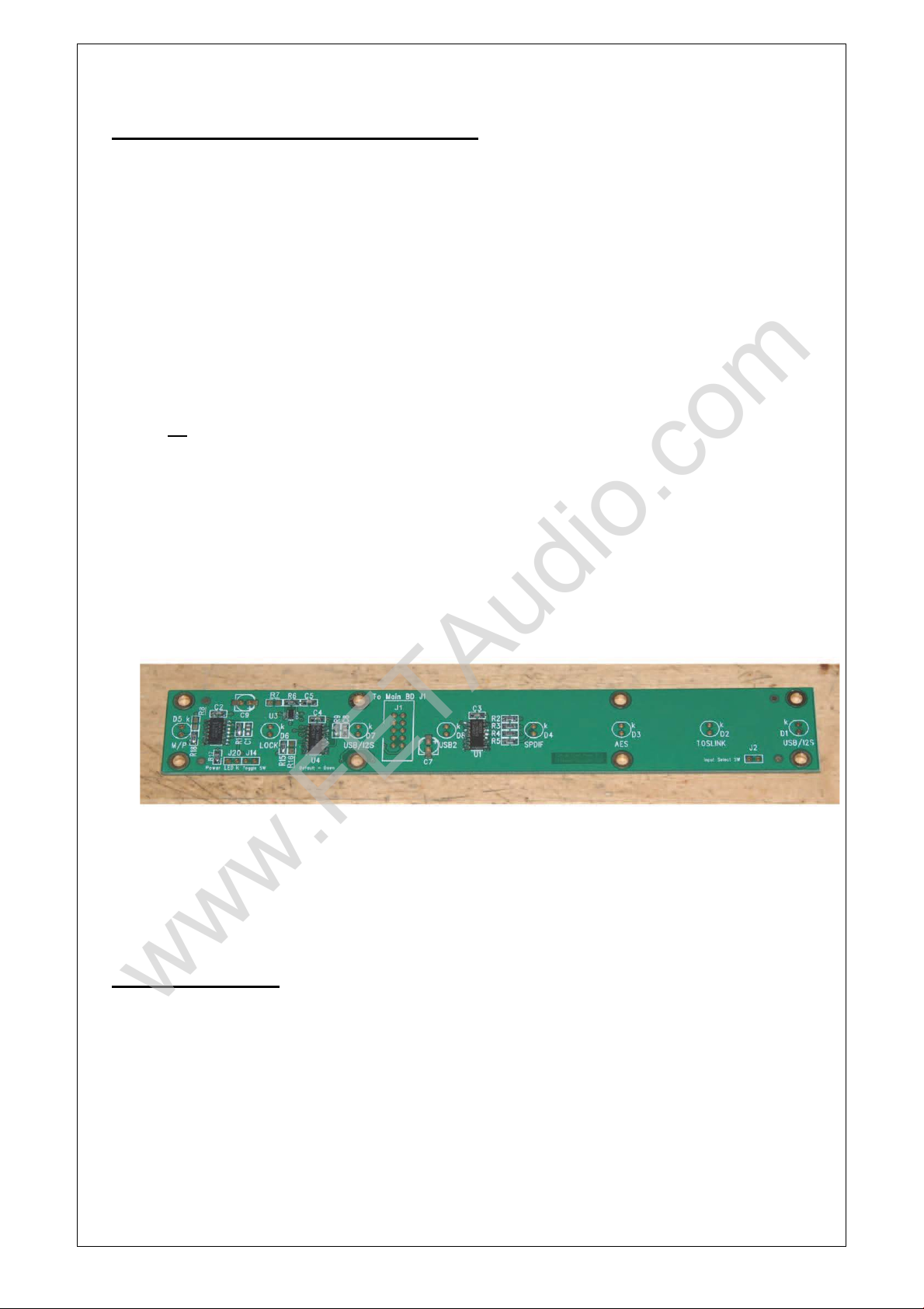
F. Front Panel Control Board (V7.1):
The front panel control board Version 7.1 will control the counting of two digits, that is
choice of 4 inputs. In FDA-2A, it can be set to use either 4 digital input (2 x SPDIF, AES &
Optical) or 3 digital input (SPDIF, AES, & Optical) and one I2S input (J5). Note that the front
panel control will remember the last selection after power off as there is a static memory
chips FM1106 on board. Short R107 and open R106 when this board is used for FDA-2A.
1. J1: Connect back to DAC main board via 10-pin flex cable.
2. J2 and J14 are the same toggle switch to select the digital input – SPDIF, AES, Toslink,
and USB/I2S (J5).
3. J20 can be connected a external Power LED. Brightness can be adjusted by changing
the value of R17.
4. R18: D5 will indicate Mute if connected. R8 should not be connected in this mode.
5. R8: D5 will be power LED indicator if connected. R18 should not be connected in this
mode.
6. The front panel can be mounted to the front plate when the LEDs are populated at
the bottom of the PCB.
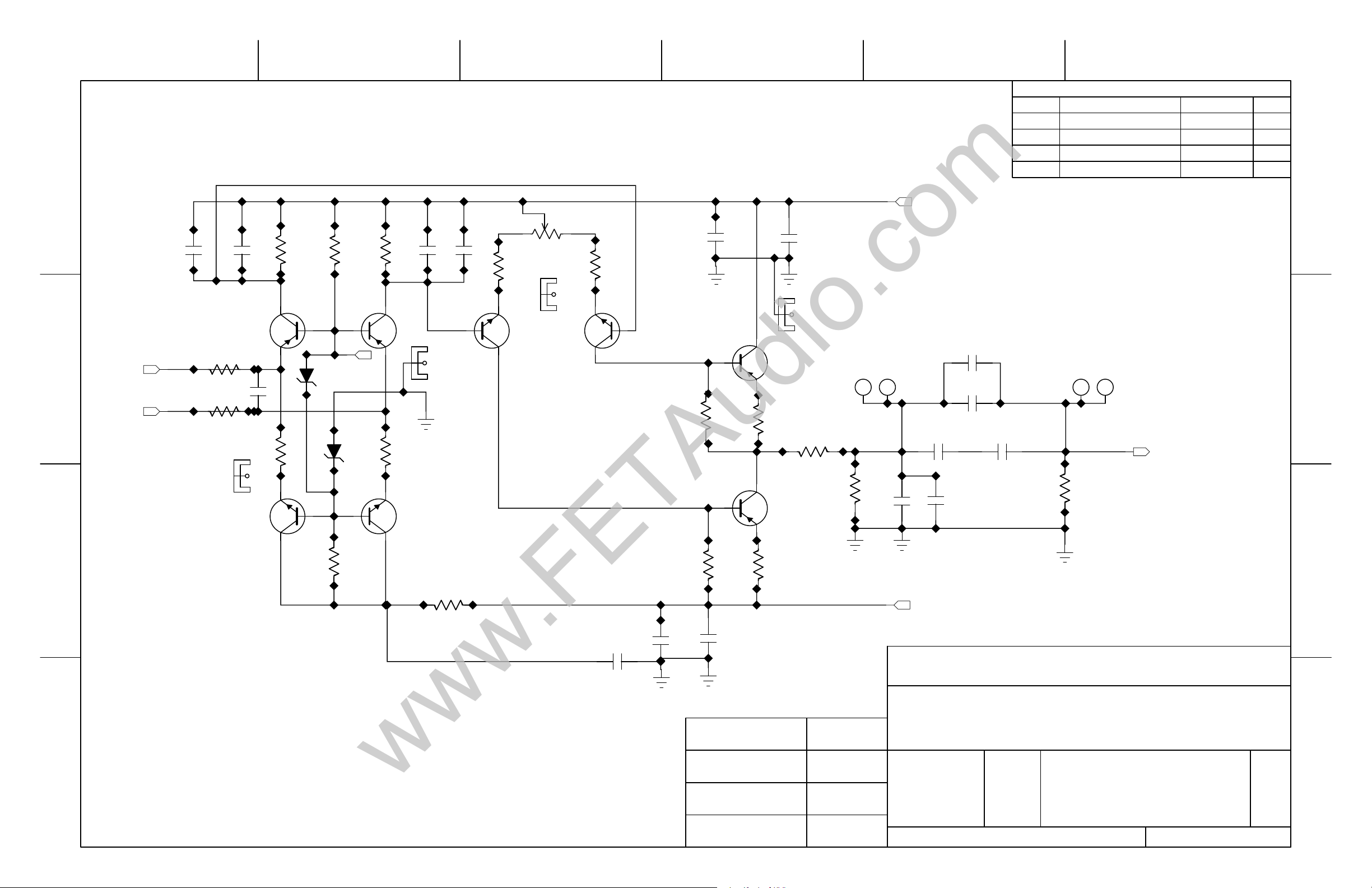
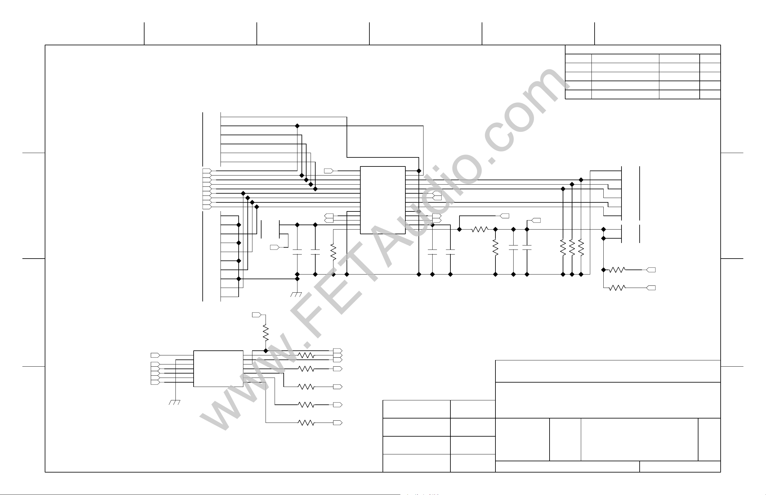
G. Attachments:
1. Circuit Diagram – 12 pages
2. BOM (Bill of Material) – 4 pages
3. FFT measurement – 9 pages
4. Jitter measurement of I2S Bus – 1 page
5. PCBs silk screen, dimension & mounting – 3 pages
~ ~ ~ E N D ~ ~ ~
www.FETAudio.com

Spencer Cheung
2012-08-15
2012-08-15
3
1955V3
FDA-2A-5
FDA-2A (AD1955 + WM8805)
Spencer Cheung
www.FETAudio.com
1
LTR
C
B
A
C
D
6
5
4
3
2
1
DATE:
D
B
A
ECO NO:
APPROVED:
REVISION RECORD
SCALE:
SHEET: OF
DRAWING NO:
TITLE:
COMPANY:
RELEASED:
DATED:
DATED:
QUALITY CONTROL:
CHECKED:
DATED:
DATED:
DRAWN:
CODE:
SIZE:
REV:
8
1:1
B
<QC Date>
<Checked Date>
<QC By>
<Checked By>
Input from PCM1794
B
B
B
Discrete IV Left
Double
R1
E
C
B
Q3
C1
R2
C2
R3
E
C
B
Q4
R4
R5
R6
E
C
B
Q5
R7
E
C
B
Q6
R8
CW
VR1
E
C
B
Q7
R9
R10
E
C
B
Q8
R11
R12
R13
R14
R15
C3
+
C4
+
C5
C6
NC
C7
NC
D2
E
C
B
Q1
E
C
B
Q2
R16
R17
+
C81
R70
C83
NC
1
H6
1
H8
1
H5
1
H7
C57
C58
C59
+
C134
J19-1
J19-2
J19-3
1
G
2
SG
3
CHS
4
S1
5
S2
6
S3
J7
RCA_JF2
C208
C209
C237
HO13
HO14
HO15
HO16
C171
C177
D60
+
C229
C234
C235
1
2
R179
1
2
R183
1
2
R187
1
2
R191
1
2
R195
1
2
R196
1
2
R203
1
2
R207
1
2
R208
1
2
R215
1
2
R216
R223
R224
R231
1
2
R235
1
2
R236
R243
R244
C246
1
G
2
SG
3
CHS
4
S1
5
S2
6
S3
J6
RCA_JF2
D1
D5
NC
C56
1
G
2
SG
3
CHS
4
S1
5
S2
6
S3
J14
RCA_JF2
+20VALL
-20VALL
LI+
LI-
GND
GND
GND
GND
OUT_LEFT
OUT_RIGHT
VREF1
www.FETAudio.comwww.FETAudio.com
3
LTR
C
B
A
C
D
6
5
4
3
2
1
DATE:
D
B
A
ECO NO:
APPROVED:
REVISION RECORD
SCALE:
SHEET: OF
DRAWING NO:
TITLE:
COMPANY:
RELEASED:
DATED:
DATED:
QUALITY CONTROL:
CHECKED:
DATED:
DATED:
DRAWN:
CODE:
SIZE:
REV:
8
2
1:1
FDA-2A-5
B
1955V3
FDA-2A (AD1955 + WM8805)
2012-08-15
<QC Date>
<Checked Date>
2012-08-15
Spencer Cheung
<QC By>
<Checked By>
Spencer Cheung
www.FETAudio.com
Input from PCM1794
Discrete IV Right
R18
E
C
B
Q9
C8
R19
C9
R20
E
C
B
Q10
R21
R22
R23
E
C
B
Q11
R24
E
C
B
Q12
R25
CW
VR2
E
C
B
Q13
R26
R27
E
C
B
Q14
R28
R29
R30
R31
R32
C10
+
C11
+
C12
C13
NC
C14
NC
D4
E
C
B
Q15
E
C
B
Q16
R33
R34
+
C82
R71
C84
NC
1
H11
1
H9
1
H10
1
H12
C60
C66
C85
+
C135
C210
C211
C238
HO9
HO10
HO11
HO12
C223
C224
D61
+
C230
C236
C241
1
2
R180
1
2
R184
1
2
R188
1
2
R192
1
2
R197
1
2
R198
1
2
R204
1
2
R209
1
2
R210
1
2
R217
1
2
R218
R225
R226
R232
1
2
R237
1
2
R238
R245
R246
C247
D3
D6
NC
C67
RI-
RI+
-20VALL
+20VALL
GND
GND
GND
GND
GND
GND
GND
GND
OUT_RIGHT
VREF2
www.FETAudio.comwww.FETAudio.com

1955V3
3
FDA-2A-5
LTR
C
B
A
C
D
6
5
4
3
2
1
DATE:
D
B
A
ECO NO:
APPROVED:
REVISION RECORD
SCALE:
SHEET: OF
DRAWING NO:
TITLE:
COMPANY:
RELEASED:
DATED:
DATED:
QUALITY CONTROL:
CHECKED:
DATED:
DATED:
DRAWN:
CODE:
SIZE:
REV:
8
3
1:1
B
FDA-2A (AD1955 + WM8805)
2012-08-15
<QC Date>
<Checked Date>
2012-08-15
Spencer Cheung
<QC By>
<Checked By>
Spencer Cheung
www.FETAudio.com
5x2 pin header
Internal I2S
External I2S Input Connector
Mute control Sel
Ext. I2S
"High = Mute"
FS (sample rate)
Mute / Lock LED drive
AD1955 Supply
I2S Mute Logic
Active Low
Active High
I2S Select
1
OE
2
A0
4
A1
6
A2
8
A3
18
Y0
16
Y1
14
Y2
12
Y3
U12-A
19
OE
11
A0
13
A1
15
A2
17
A3
9
Y0
7
Y1
5
Y2
3
Y3
U12-B
2
3
1
U13-A
5
6
4
U13-B
8
9
10
U13-C
11
12
13
U13-D
1
2
3
U14-A
4
5
6
U14-B
9
10
8
U14-C
12
13
11
U14-D
R90
1
2
L11
1
2
L12
J5-1
J5-2
J5-3
J5-4
J5-5
J5-6
J5-7
J5-8
J5-9
J5-10
1
2
L15
1
2
R93
1
2
R94
1
2
R95
1
2
R96
C196
C198
1
2
R64
1
2
R76
R84
1
2
R171
1
2
L10
+
C17
+
C22
C23
C24
3
IN
2
OUT
1
G
4
U1
AMS1117-5
C15
C18
C16
C44
1
2
L2
1
2
L8
1
2
R53
1
2
R88
C54
C55
J30-1
J30-2
1
2
R108
1
2
R120
1
2
R121
+5VDAC
E_LRCK
E_BCLK
E_SDA
E_MCLK
I_MUTE
I2S2
LOCK
DGND
GND
I_LRCLK
I_BCLK
I_SDATA
I_MCLK
DGND
+5VREG
MUTE_MS_B
IMUTE
+5VDAC
1955AVDD
+3.3VD
RESET
MCLK
SDATA
BCLK
LRCLK
MUTE_B
LOCKO
I2S1
DGND
+12VDC
1955DVDD
DGND
LRCLK
I2S2
E_MUTE
USB2
USB
www.FETAudio.comwww.FETAudio.com
3
LTR
C
B
A
C
D
6
5
4
3
2
1
DATE:
D
B
A
ECO NO:
APPROVED:
REVISION RECORD
SCALE:
SHEET: OF
DRAWING NO:
TITLE:
COMPANY:
RELEASED:
DATED:
DATED:
QUALITY CONTROL:
CHECKED:
DATED:
DATED:
DRAWN:
CODE:
SIZE:
REV:
8
4
1:1
FDA-2A-5
B
1955V3
FDA-2A (AD1955 + WM8805)
2012-08-15
<QC Date>
<Checked Date>
2012-08-15
Spencer Cheung
<QC By>
<Checked By>
Spencer Cheung
www.FETAudio.com
NOS or ASRC MODULE
DAC
I2S Bus
SPI Bus
DSD Bus
VREF
J15 and J17: Test point for Vref
1
+5VREG
2
DGND
3
IMUTE
4
ILRCK
5
ISCLK
6
ISDATA
7
IMCK
8
MCKO
9
SDATAO
10
SCLKO
11
LRCKO
12
MUTEO
13
RESET
14
GND
U18
1
2
R154
1
2
R153
1
2
R152
1
2
R151
R79
1
DVDD
2
LRCLK
3
BCLK
4
SDATA/L
5
/RDATA
6
DSD_SCLK
7
DSD_LDATA
8
DSD_RDATA
9
DSD_PHASE
10
AGND1
11
IOUTR+
12
IOUTR-
13
FILTR
14
IREF
28
DGND
27
MCLK
26
CCLK
25
CLATCH_BAR
24
CDATA
23
PD/RST_BAR
22
MUTE
21
ZEROL
20
ZEROR
19
AGND2
18
IOUTL+
17
IOUTL-
16
FILTB
15
AVDD
U11
1
2
R41
C43
C45
1
2
R42
1
2
R44
1
2
R47
1
2
R35
1
2
R45
C50
+
C19
+
C20
+
C21
J12-1
J12-2
J12-3
J12-4
J13-1
J13-2
J13-3
J13-4
J13-5
J15-1
J15-2
J13-6
J16-1
J16-2
J16-3
J16-4
J16-5
J12-5
J12-6
J16-6
J16-7
J16-8
J16-9
J16-10
J17-1
J17-2
1
2
R46
1
2
R48
1
2
R123
MCLK
SDATA
BCLK
LRCLK
+5VREG
DGND
IMUTE
RESET
MUTE_MS_B
LRCKO
BCLKO
SDATAO
MCKO
+3.3VD
LI+
LI-
RI+
RI-
LRCKO
BCLKO
SDATAO
MUTE_MS_B
RESET
1955AVDD
1955DVDD
DGND
MCKO
RDATAO
DSD_SCLK
DSD_LDATA
DSD_RDATA
DSD_PHASE
VREF
VREF
VREF1
VREF2
RDATAO
www.FETAudio.comwww.FETAudio.com

3
2012-08-15
2012-08-15
1955V3
FDA-2A-5
LTR
C
B
A
C
D
6
5
4
3
2
1
DATE:
D
B
A
ECO NO:
APPROVED:
REVISION RECORD
SCALE:
SHEET: OF
DRAWING NO:
TITLE:
COMPANY:
RELEASED:
DATED:
DATED:
QUALITY CONTROL:
CHECKED:
DATED:
DATED:
DRAWN:
CODE:
SIZE:
REV:
8
5
1:1
B
FDA-2A (AD1955 + WM8805)
<QC Date>
<Checked Date>
Spencer Cheung
<QC By>
<Checked By>
Spencer Cheung
www.FETAudio.com
Output Muting Ckt
Mute Relays
RCA2
RCA1
AES
TOSLINK
Digital input select
H/W-Mode
8805 Ctrl Bus
8805 RxGx Bus
C62
R86
1
2
R72
1
2
R73
1
2
R74
1
2
R82
C86
1
2
R83
D21
1
2
3
4
5
6
7
8
K1
EC2-12V
R251
C258
E
C
B
Q31
E
C
B
Q33
E
C
B
Q32
+
C263
J26-1
J26-2
J26-3
J26-4
J26-5
J26-6
J26-7
J26-8
J26-9
J26-10
J29-1
J29-2
J29-3
J29-4
J29-5
J29-6
J29-7
J29-8
J29-9
J29-10
1
2
R102
1
2
R103
1
2
R104
1
2
R105
2
1
3
U2-A
5
4
6
U2-B
9
10
8
U2-C
12
13
11
U2-D
C89
C91
NC
J32-1
J32-2
1
2
U15-A
3
4
U15-B
5
6
U15-C
9
8
U15-D
11
10
U15-E
13
12
U15-F
C92
NC
R109
R110
R111
C93
OUT_LEFT
GND
PWROFFCTL
LOCK
+20VALL
GND
RL+
RL-
OUT_RIGHT
RL+
RL-
+20VAR
AGND
CSB
SDOUT
SDIN
GPO0/SWIFM
SCLK
GPO1
RX4/GPO3
RX5/GPO4
RX6/GPO5
RX7/GPO6
DGND
+3.3VD
I1
I2
I4
I3
RX03
RX02
RX01
RX00
DGND
RX0
www.FETAudio.comwww.FETAudio.com
Table of contents
Popular Media Converter manuals by other brands


H&B
H&B TX-100 Installation and instruction manual

Bolin Technology
Bolin Technology D Series user manual

IFM Electronic
IFM Electronic Efector 400 RN30 Series Device manual

GRASS VALLEY
GRASS VALLEY KUDOSPRO ULC2000 user manual

Linear Technology
Linear Technology DC1523A Demo Manual

Lika
Lika ROTAPULS I28 Series quick start guide

Weidmuller
Weidmuller IE-MC-VL Series Hardware installation guide

Optical Systems Design
Optical Systems Design OSD2139 Series Operator's manual

Tema Telecomunicazioni
Tema Telecomunicazioni AD615/S product manual

KTI Networks
KTI Networks KGC-352 Series installation guide

Gira
Gira 0588 Series operating instructions

Lika
Lika SFA-5000-FD user guide