manuals.online logo
Brands
  1. Home
  2. •
  3. Brands
  4. •
  5. Fuji Electric
  6. •
  7. Computer Hardware
  8. •
  9. Fuji Electric OPC-G1-PG22 User manual

Fuji Electric OPC-G1-PG22 User manual

- 1 -
PG インタフェース(5V ラインドライバ)カード「OPC-G1-PG22」
PG インタフェース(5V ラインドライバ)カード(以降,PG インタフェースカード)「OPC-G1-PG22」をお買上げいただきましてあ
りがとうございます。この PG インタフェースカードを FRENIC-MEGA に取り付けることで,PG を使用した 2 台のモータの同期運転
や、パルス列入力による周波数指令などが可能となります。
・このカードを搭載する場合は、インバータ本体端子 X7 のパルス列入力は使用できません。
・FRENIC-MEGA にはオプション接続ポートが 3 箇所あります(A,B,C-Port)。この PG インタフェースカードは,C-Port
へ取り付けてください(A,B-Port には取付けできません)。また、本カードの取付けにより B-Port のスペースも占有
するため、B-Port への他のオプションカードの取付けはできなくなります。
1. 製品の確認
次の項目を確認してください。
(1) PG インタフェースカードおよび,ねじ(M3×8:4 本)
が入っていることを確認してください。
(2) PG インタフェースカード上の部品の異常,凹み,反り
など輸送時での破損がないことを確認してください。
(3) PG インタフェースカード上に形式「OPC-G1-PG22」が
印刷されていることを確認してください。(図 1-1)
製品にご不審な点や不具合などございましたら,お買上げ
店または最寄りの弊社営業所までご連絡ください。
図 1-1 各部名称(カード表面) 図 1-2 各部名称(カード裏面)
2. 取付け方法
取付け・配線は電源を遮断して 22kW 以下は 5 分以上,30kW 以上は 10 分以上経過してから行ってください。更に LED モニタおよ
びチャージランプの消灯を確認し,テスターなどを使用して主回路端子 P(+)-N(-)間の直流中間回路電圧が安全な値(DC+25V 以
下)に下がっていることを確認してから行ってください。
感電のおそれあり
(1) インバータ本体の表面カバーを取り外し,制御プリント基板を露出させてください。本 PG インタフェースカードは
C-Port(CN6)にのみ取付け可能です。(図 2-1)
 FRENIC-MEGA 取扱説明書の「2.3 配線」を参照して表面カバーを取り外してください。
(30kW 以上はタッチパネルケースも開けてください。)
(2) PG インタフェースカードの裏面(図 1-2)の CN1 をインバータ本体の制御プリント基板の C-Port(CN6)へ差し込み,付属
ねじで固定してください。(図 2-3)
PG インタフェースカードの取付け位置決め部(図 1-1)がツメ(図 2-2①)にセットされ,CN1(図 2-3②)が確実に差し込
まれていることを確認してください。図 2-3 は取付け完了を示します。本インタフェースカードは C-Port 以外に取
り付けないでください。接続すると破損する可能性があります。
(3) PG インタフェースカードの配線を行います。
 「3 配線」を参照してください。
(4) インバータ本体の表面カバーを元に戻してください。
 FRENIC-MEGA 取扱説明書の「2.3 配線」を参照して表面カバーを取り付けてください。
(30kW 以上はタッチパネルケースも閉じてください。)
①カードの取付け位置決め部をインバータ本
体のツメに合わせ,取付け位置を決めます。
②カード裏面の CN1 を,インバータ本体の制御
プリント基板の C-Port(CN6)へ差し込みます。
図 2-1 取付け可能ポート 図 2-2 カードの取付け 図 2-3 取付け完了
ねじ取付け用穴(左)
ねじ取付け用穴(右)
J1
CN1
正式形式
取付け位置決め部
取外し用つまみ
c
②
CN6
CN5CN4
A
-Port
取付
け
可能
(B-port も占有)
取付け不可
A
-Port
B-Port
C-Port
SW1
- 2 -
3. 配線
一般的に制御信号線の被覆は強化絶縁されていませんので,主回路活電部に制御信号線が直接触れると,何らかの原因で絶縁被
覆が破壊されることがあります。この場合,制御信号線に主回路の高電圧が印加される危険性がありますので,主回路活電部に
制御信号線が触れないように注意してください。
事故のおそれあり,感電のおそれあり
インバータ,モータ,配線からノイズが発生します。周辺のセンサーや機器の誤動作防止対策をとってください。
事故のおそれあり
PG インタフェースカードへ の 配 線 は ,下 記 の 端子配置図(図 3-1),端子仕様(表 3-1),回路構成(図 3-2)および配線方法(図 3-3)を
参照して行ってください。
PG インタフェースカードと PG の配線はシールド線を使用し,100m 以内としてください。シールド線のシールドは PG インタフ
ェースカードの CM 端子に接続し,PG 側は開放とすることを推奨します。ノイズによる誤動作が問題になる場合は、シールド線
を 1~2 ターン程度、フェライトコアに貫通させることで改善する場合があります。
ノイズによる誤動作を防ぐため,PG インタフェースカードの配線は,主回路の配線とは可能な限り離して配線してくださ
い。インバータ内部の PG インタフェースカードの配線は,主回路活電部(例えば主回路端子台部)に直接接触しないよう
に内部で束線固定などの処理を行ってください。
7.5kW の例
配線はインバータ本体の制御端子台と
表面カバーの間を通してください。
図 3-3 配線方法
75kW の例
表 3-1 端子仕様
端子サイズ M2
締付トルク 0.22~0.25N・m
適用電線サイズ *1 AWG16~24
むき線長さ 6~7mm
*1 電線は許容温度 105℃(UL 対応品)絶縁電線を推奨します。
フォトカプラ
DC+5V
INTEXT
PO
PI
YA,YB,YZ,
XA,XB,XZ
CM
J1
*YA,*YB,*YZ,
*XA,*XB,*XZ
フォトカプラ
インタフェース回路
断線検出回路
DC+5V
CM
CM
PO
シールド線のシールドは CM 端子へ接
続してください。CM 端子が足りない場
合は、共締めしてください。
ケーブルの接続(拡大図)
図 3-1 端子配置図
図 3-2 回路構成
- 3 -
4. 仕様
PG インタフェース仕様を表 4-1 に示します。
表 4-1 PG インタフェース仕様
項 目 仕 様
適用 PG
出力パルス数 20~ 3000P/R
最大応答周波数 100kHz
パルス出力方式 ラインドライバ方式(26C31,26LS31 相当)
ソース電流 +20mA(MAX)/シンク電流 -20mA(MAX)
最大配線長 100m
PG 電源 DC+5V±10%/300mA 以下 *1
*1 PG の消費電流が 300mA を超える場合は外部電源を使用してください。
5. 端子機能
端子機能一覧を表 5-1 に示します。
表 5-1 端子機能一覧
端子記号 端子名称 端子機能説明
電源
PI 外部電源入力端子 *1
PG 用の電源を外部から入力する端子
DC+5V±10%入力 *2
(接続する電源は PG 電源の消費電流以上を確保してください。)
PO 内部電源出力端子 *4 PG 用の電源を出力する端子
DC+5V-0%~+10%/300mA 出力 *3
CM コモン端子 *5 PG 用の電源コモン端子
(インバータ本体の端子 CM と同電位です。)
PG/パルス入力
YA YA(+)相パルス入力端子 追従側 PG の A 相(+)信号を入力する端子
*YA YA(-)相パルス入力端子 追従側 PG の A 相(-)信号を入力する端子
YB YB(+)相パルス入力端子 追従側 PG の B 相(+)信号を入力する端子
*YB YB(-)相パルス入力端子 追従側 PG の B 相(-)信号を入力する端子
YZ YZ(+)相パルス入力端子 追従側 PG の Z 相(+)信号を入力する端子
*YZ YZ(-)相パルス入力端子 追従側 PG の Z 相(-)信号を入力する端子
XA XA(+)相パルス入力端子 基準側 PG の A 相(+)信号を入力する端子
*XA XA(-)相パルス入力端子 基準側 PG の A 相(-)信号を入力する端子
XB XB(+)相パルス入力端子 基準側 PG の B 相(+)信号を入力する端子
*XB XB(-)相パルス入力端子 基準側 PG の B 相(-)信号を入力する端子
XZ XZ(+)相パルス入力端子 基準側 PG の Z 相(+)信号を入力する端子
*XZ XZ(-)相パルス入力端子 基準側 PG の Z 相(-)信号を入力する端子
*1 PG の消費電流が 300mA を超える場合は外部電源を使用してください。外部電源を使用する場合はジャンパ J1 を EXT 側に
接続してください。( 「6.設定」を参照してください。)
*2 PG の許容電圧範囲に合った外部電源を使用してください。外部電源電圧は PG との配線インピーダンスによる電圧降下を
考慮し PI の電圧範囲内(上限+10%)で調整するか,配線線径を太くしてください。(表 5-2 を参照してください。)
*3 PG との配線インピーダンスによる電圧降下により PG の許容電圧範囲を下回る場合は、外部電源を使用するか、配線線径
を太くしてください。
*4,*5 PO 端子は 2 つ、CM 端子は 3 つありますが、PG インタフェースカード内部でそれぞれ導通しております。
表 5-2 推奨配線径
PG 電源仕様 配線長[m]
~20 ~30 ~50 ~75 ~100
5V±10%,300mA AWG24
(0.25mm2)
AWG22
(0.34mm2)
AWG20
(0.50mm2)
AWG18
(0.75mm2)
AWG16
(1.25mm2)
- 4 -
6.設定
6-1.PG 電源の設定
インバータの電源を入れる前に、PG に供給する電源の設定をジャンパ J1 で行ってください。内部電源と外部電源との切り替えを
行います。表 6-1,図 6-1 を参照してください。
表 6-1 PG に供給する電源の設定
使用電源 切り替えキャップの設定
内部電源
(工場出荷状態)
ジャンパ J1 の INT 側を切替キャップにより短絡してください。
(負荷電流 Max.300mA でご使用ください。)
外部電源 ジャンパ J1 の EXT 側を切替キャップにより短絡してください。
端子 PI に DC+5V±10%の電源を接続してください。
J1
INT EXT
切替キャップ
J1
INT EXT
切替キャップ
内部電源使用時(工場出荷状態) 外部電源使用時
図 6-1 ジャンパ J1 の設定
6-2.断線検出機能の有効/無効切り替え
本 PG インターフェースカードには、PG 線の断線を検出する断線検出機能があります。YZ,XA,XB,XZ 相の断線検出機能は各相
についてそれぞれ有効/無効を切り替え可能です。表 6-2 を参照して、SW1 の設定を行ってください。なお YA,YB 相の断線検出
機能は常に有効ですので、YA,YB 相を使用しない場合はそれぞれの(+)信号を PO 端子に、(-)信号を CM 端子に接続してください。
表 6-2 断線検出機能の有効/無効の切り替え
切替対象 SW1 のピン№
断線検出機能 *1
有効
(工場出荷状態) 無効
YZ 相 1 OFF ON
XA 相 2 OFF ON
XB 相 3 OFF ON
XZ 相 4 OFF ON
*1 信号線を接続しないとき、または接続しても使用しないときは、
“ON“側に設定してください。
・ スイッチの切換は,先端の細い治具(ピンセット
先端など)を使用して,他の電子部品などに触れ
ないよう注意して行ってください。
・スライダはしっかりと確実に端まで押し込んで
ください。
INT
EXT
J1
ON
SW1
OFF
- 5 -
7.対応する制御方式
本 PG インタフェースカードを FRENIC-MEGA に取り付けることで,PG を使用した 2 台のモータの同期運転や、パルス列入力によ
る周波数指令などが可能となります。各制御方式に対応可能なインバータ型式および ROM バージョンは表 7-1 を参照してくださ
い。パルス列入力運転の詳細設定は FRENIC-MEGA 取扱説明書・ユーザーズマニュアルを、同期運転の詳細設定は同梱の同期運転
マニュアルを参照してください。
表7-1 適用インバータ型式と ROM バージョン
制御方式 機種
型式
インバータ
容量
ROM
バージョン
PG/パルス入力 *1
F42/A14/b14/r14 *2 追従側(Y) 基準側(X)
パルス列入力運転
0: V/f 制御:滑り補償なし
FRENIC-MEGA
*4
FRN□□□G1□-□□□
全容量 3510 以降
× ○
1: ダイナミックトルクベクトル制御 × ○
2: V/f 制御:滑り補償あり × ○
3: 速度センサ付き V/f 制御 ○ ○
4: 速度センサ付きダイナミック
トルクベクトル制御 ○ ○
5: 速度センサレスベクトル制御 × ○
6: 速度センサ付きベクトル制御 ○ ○
同期運転
3: 速度センサ付き V/f 制御 ○ ○
4: 速度センサ付きダイナミック
トルクベクトル制御 ○ ○
6: 速度センサ付きベクトル制御 ○ ○
*1 ○:接続必要 ×:接続不要
*2 機能コード”F42/A14/b14/r14:制御方式選択”の詳細は、FRENIC-MEGA 取扱説明書を参照ください。
*3 ラインドライバ方式出力のパルス列発生器による、PG 付きモータの周波数制御が可能です。
*4 □には,インバータ容量,タイプ,電圧シリーズなどを示す英数字が入ります。
インバータの ROM バージョンは,プログラムモードのメニュー番号5「メンテナンス情報」の 5_14 で確認することができます。
詳細は,FRENIC-MEGA 取扱説明書の第3章「3.4.6 メンテナンス情報を見る」を参照してください。
LED モニタの表示 項目 表示内容
5_14
インバータ ROM バージョン インバータの ROM バージョンを 4 桁で表示します。
*3
- 6 -
7-1.同期運転時の接続例
同期運転時の接続例を図 7-1 に示します。基準側モータと追従側モータの同期運転が可能になります。
図 7-1 同期運転時の接続図
・ PG とインバータ間の配線にはシールド線を使用してください。シールド線のシールドは PG インターフェースカードの CM
端子に接続し、PG 側は開放とすることを推奨します。
・ PG とインバータ間の配線が長い場合,A 相と B 相の干渉により PG からの信号が誤動作し異音やトルク脈動が発生する場合
があります。この場合は,配線を極力短くしたり(配線経路の見直し),浮遊容量の小さなケーブルを使用する等で改善さ
れる場合もあります。
・ PG インタフェースカード上の J1 は,内部電源使用時:INT,外部電源使用時:EXT に設定してください。
・ ノイズによる誤動作が問題になる場合は、シールド線を 1~2 ターン程度、フェライトコアに貫通させることで改善する場
合があります。
・ このカードを搭載する場合は、インバータ本体端子 X7 のパルス列入力機能は使用できません。
富士電機株式会社 パワエレ機器事業本部 ドライブ事業部
〒141-0032 東京都品川区大崎一丁目 11 番 2 号 (ゲートシティ大崎イーストタワー)
URL http://www.fujielectric.co.jp/
発行 富士電機株式会社 鈴鹿工場 〒513-8633 三重県鈴鹿市南玉垣町 5520 番地
技術相談窓口 TEL:0120-128-220 FAX:0120-128-230
INR-SI47-1475b-JE
Ⅰ.インバータ内部電源使用時
OPC-G1-PG22
Ⅱ.外部電源使用時
FRENIC-MEGA
OPC-G1-PG22
5Vdc ±10%
FRENIC-MEGA
PO
YA
PO
CM
PI
U
V
W
M M
基準側
追従側 U
V
W
M M
基準側
追従側
L1/R
PO
PO
PI
G
G
L2/S
L3/T
L1/R
L2/S
L3/T
EXTINT
J1
EXTINT
J1
*YA
YB *YB
YZ *YZ
PG
XA
CM
*XA
XB *XB
XZ *XZ
PG
YA
CM
*YA
YB *YB
YZ *YZ
XA
CM
*XA
XB *XB
XZ *XZ
PG
PG
ON
OFF
SW1
1 2 3 4
ON
OFF
SW1
1 2 3 4
- 7 -
Instruction Manual
PG Interface (5 V Line Driver) Card "OPC-G1-PG22"
Thank you for purchasing this PG interface card containing 5 V line driver card (hereinafter called PG interface card), "OPC-G1-PG22."
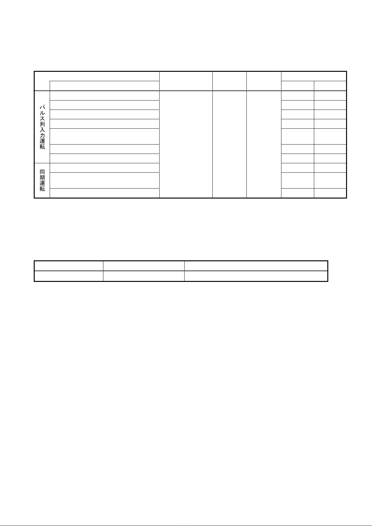
Mounting this card on your FRENIC-MEGA enables synchronous operation of two motors using PGs or frequency command entry by
pulse train input.
・Mounting this interface card disables the pulse train input function assigned to the inverter's [X7] terminal.
・The FRENIC-MEGA has three option connection ports--A-, B-, and C-ports. Connect this PG interface card to the C-port.
The A- and B-ports cannot accept this card. Mounting this card occupies also the B-port space so that any option card canno
t
be connected to the B-port.
1 Check that:
(1) A PG interface card and four screws (M3 ×8) are
contained in the package.
(2) The PG interface card is not damaged during
transportation--no defective devices, dents or warps.
(3) The model name "OPC-G1-PG22" is printed on the PG
interface card. (See Figure 1.1.)
If you suspect the product is not working properly or if you
have any questions about your product, contact the shop where
you bought the product or your local Fuji branch office.
Figure 1.1 Front of Card Figure 1.2 Back of Card
2 Installation
Before starting installation and wiring, turn OFF the power and wait at least five minutes for inverters with a capacity of 22 kW or
below, or at least ten minutes for inverters with 30 kW or above. Make sure that the LED monitor and charging lamp are turned OFF.
Further, make sure, using a multimeter or a similar instrument, that the DC link bus voltage between the terminals P(+) and N(-) has
dropped to the safe level (+25 VDC or below).
Otherwise, electric shock could occur.
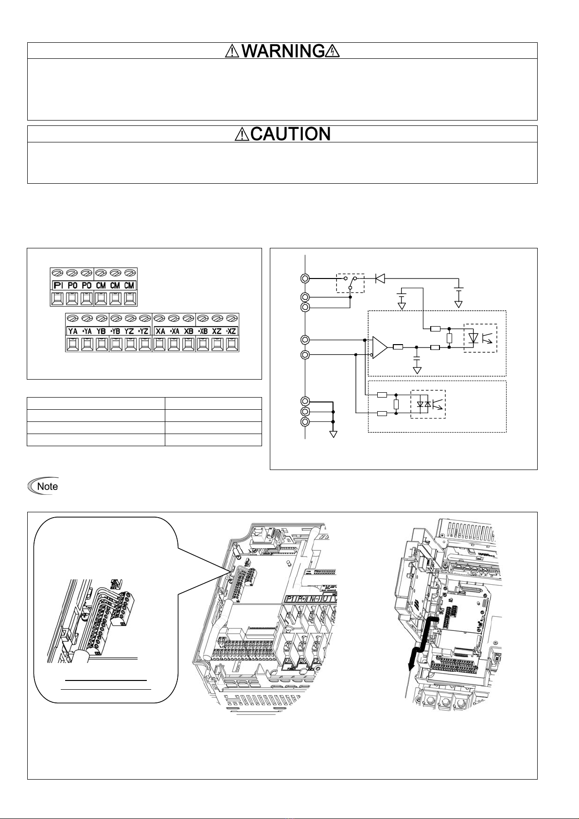
(1) Remove the front cover from the inverter and expose the control printed circuit board (control PCB). The PG interface card can be
connected to the C-port (CN6) only. (Figure 2.1)
To remove the front cover, refer to the FRENIC-MEGA Instruction Manual, Section 2.3. For inverters with a capacity of 30 kW or
above, open also the keypad enclosure.
(2) Insert connector CN1 on the back of the PG interface card (Figure 1.2) into the C-port (CN6) on the inverter's control PCB. Then
secure the card with the four screws that come with the card. (Figure 2.3)
Check that the positioning cutout (Figure 1.1) is fitted on the tab (cin Figure 2.2) and connector CN1 is fully inserted
(din Figure 2.3). Figure 2.3 shows the PG interface card correctly mounted. Do not connect the interface card to the
p
orts other than C-port. Doing so may damage the card.
(3) Perform wiring to the PG interface card.
Refer to Section 3 "Wiring."
(4) Put the front cover back into place.
To put back the front cover, refer to the FRENIC-MEGA Instruction Manual, Section 2.3. For inverters with a capacity of 30 kW or
above, close also the keypad enclosure.
Figure 2.1 Option Connection Ports Figure 2.2 Mounting PG Interface Card Figure 2.3 Mounting Completed
c
Screw holes (right)
J1
CN1
Model name
Positioning cutout
Release knob
Screw holes (left)
SW1
①Fit the positioning cutout of the card over
the tab on the inverter to determine the
mounting position.
②Insert connector CN1 on the card into
the C-port (CN6) on the inverter's
control PCB.
②
CN6
CN5
CN4
C-Port
B-Port
A
-Port
A
va
il
a
bl
e
(B port also
occupied)
Not available
- 8 -
3 Wiring
In general, the covers of the control signal wires are not specifically designed to withstand a high voltage (i.e., reinforced insulation is
not applied). Therefore, if a control signal wire comes into direct contact with a live conductor of the main circuit, the insulation of the
cover might break down, which would expose the signal wire to a high voltage of the main circuit. Make sure that the control signal
wires will not come into contact with live conductors of the main circuit.
Failure to observe these precautions could cause electric shock or an accident.
Noise may be emitted from the inverter, motor and wires.
Take appropriate measures to prevent the nearby sensors and devices from malfunctioning due to such noise.
An accident could occur.
Perform wiring to the PG interface card, referring to the "Terminal Allocation and Symbol Diagram" (Figure 3.1), "Terminal
Specifications" (Table 3.1), "Internal Block Diagram" (Figure 3.2), and "Wiring Instructions" (Figure 3.3) given below.
For wiring between the PG interface card and the PG(s), use a shielded cable having a length of 100 m or below. It is recommended that
the shielded layer be connected to the [CM] terminal on the card and be open at the PG side. If malfunctioning due to noise causes a
problem, winding the shielded cable around a ferrite core by one or two turns may reduce the problem.
Figure 3.1 Terminal Allocation and Symbol Diagram
Photocoupler
+5 VDC
INTEXT
PO
PI
YA, YB,YZ,
XA, XB,XZ
CM
J1
*YA, *YB, *YZ,
*XA,*XB,*XZ
Photocoupler
I/F circuit
Wire break
detection circuit
+5 VDC
CM
CM
PO
Figure 3.2 Internal Block Diagram
Table 3.1 Terminal Specifications
Terminal Size M2
Tightening Torque 0.22 to 0.25 N·m
Recommended Wire *1AWG16 to 24
Wire strip length 6 to 7 mm
*1Insulated wires with allowable temperature of 105ºC (UL-listed)
are recommended.
To prevent malfunctioning due to noise, separate the wires of the interface card as far apart as possible from those for the main
circuits. Also, inside the inverter, bundle and fix the wires of the interface card so that they do not come into direct contact with
the main circuit terminal block or other live parts of the main circuits.
In the case of 7.5 kW In the case of 75 kW
Pass the wires from the PG interface cardbetween
the control circuit terminal block and the front cover.
Figure 3.3 Wiring Instructions
Connect the shielded layer to a
[CM] terminal.
If [CM] terminals are lacking, share
a single terminal with two wires and
tighten them together.
Connecting the cable to
terminals (magnified view)
- 9 -
4 Specifications
Table 4.1 lists the specifications of the PG interface card.
Table 4.1 PG Interface Card Specifications
Item Specifications
Applicable PG
Pulse resolution 20 to 3000 P/R
Maximum response frequency 100 kHz
Pulse output system Line driver (Equivalent to 26C31 or 26LS31)
Source current: +20 mA (max.), Sink current: -20 mA(max.)
Maximum wiring length 100 m
PG power supply +5 VDC ±10%, 300 mA or below *1
*1When the PG current consumption exceeds 300 mA, use an external power supply.
5 Terminal Functions
Table 5.1 lists terminal symbols, names and functions of the option terminals on the PG interface card.
Table 5.1 Option Terminals and Their Specifications
Terminal symbol Name Functions
Power supply
PI External power supply input*1
Power input terminal from the external device for the PG
+5 VDC ±10% input *2
(A power supply to be connected should assure the PG current consumption or
larger.)
PO Internal power supply output*4Power output terminal for the PG
+5 VDC -0% to +10%, 300 mA output *3
CM PG power common *5Common terminal for power supply for PG
(Equipotent with [CM] terminal of the inverter)
PG/pulse input
YA YA(+) phase pulse input from slave PG Input terminal for A(+) phase signal fed back from the slave PG
*YA YA(-) phase pulse input from slave PG Input terminal for A(-) phase signal fed back from the slave PG
YB YB(+) phase pulse input from slave PG Input terminal for B(+) phase signal fed back from the slave PG
*YB YB(-) phase pulse input from slave PG Input terminal for B(-) phase signal fed back from the slave PG
YZ YZ(+) phase pulse input from slave PG Input terminal for Z(+) phase signal fed back from the slave PG
*YZ YZ(-) phase pulse input from slave PG Input terminal for Z(-) phase signal fed back from the slave PG
XA XA(+) phase pulse input from reference PG Input terminal for A(+) phase signal fed back from the reference PG
*XA XA(-) phase pulse input from reference PG Input terminal for A(-) phase signal fed back from the reference PG
XB XB(+) phase pulse input from reference PG Input terminal for B(+) phase signal fed back from the reference PG
*XB XB(-) phase pulse input from reference PG Input terminal for B(-) phase signal fed back from the reference PG
XZ XZ(+) phase pulse input from reference PG Input terminal for Z(+) phase signal fed back from the reference PG
*XZ XZ(-) phase pulse input from reference PG Input terminal for Z(-) phase signal fed back from the reference PG
*1 When the PG current consumption exceeds 300 mA, use an external power supply and set a jumper cap at the EXT side on jumper J1. (Refer to
Section 6 "Configuration".)
*2Use an external power supply whose rating meets the allowable voltage range of the PG. Regulate the external power supply voltage within the PI
voltage range (upper limit +10%), taking into account the voltage drop caused by the PG-inverter wiring impedance. Or, use a wire with a larger
diameter. (Refer to Table5.2)
*3If the PO voltage level falls below the allowable voltage range of the PG due to voltage drop caused by PG-inverter wiring impedance, use an
external power supply or a wire with a larger diameter.
*4 *5 The PG interface card has two [PO] terminals and three [CM] terminals, each of which is conducting inside the card.
Table 5.2 Recommended Wire Size
PG power supply
requirements Wiring length (m)
Up to 20 Up to 30 Up to 50 Up to 75 Up to 100
5 V ±10%,300 mA AWG24
(0.25 mm2) AWG22
(0.34 mm2) AWG20
(0.50 mm2) AWG18
(0.75 mm2) AWG16
(1.25 mm2)
- 10 -
6 Configuration
6.1 Switching between internal and external power supplies for PGs
Before powering on the inverter, switch between internal and external power supplies for the PGs using jumper J1, referring to Table 6.1
and Figure 6.1.
Table 6.1 Internal and External Power Supplies for PGs
Power Supply Short-circuit jumper J1 using a jumper cap
Internal power supply
(Factory default) At the INT side
(Use the power supply with max. 300 mA load current.)
External power supply At the EXT side
Connect +5 VDC ±10% power to the [PI] terminal.
J1
INT EXT
Jumper cap
J1
INT EXT
Jumper cap
When using an internal power supply When using an external power supply
(Factory default)
Figure 6.1 Configuration of Jumper J1
6.2 Enabling/disabling the wire break detection function with DIP SW1
The PG interface card has a wire break detection function that detects wire breaks in the PG cable. It is possible to enable/disable this
detection function in each of the YZ, XA, XB, and XZ phases. Please refer to Table 6.2 when enabling/disabling the detection function
for each phase with the DIP SW1.
Note that the wire break detection function of the YA and YB phases is always enabled. When not using these phases, connect their
respective (+) phases to the [PO] terminals and their respective (-) phases to the [CM] terminals.
Table 6.2 Enabling/Disabling the Wire Break Detection Function
Target Selector No. on DIP SW1 Wire Break Detection Function *1
To enable
(Factory default) To disable
YZ phase 1 OFF ON
XA phase 2 OFF ON
XB phase 3 OFF ON
XZ phase 4 OFF ON
*1When a particular signal line is not to be connected or not to be used even if connected,
turn the corresponding selector to the ON position.
・To move selectors on the DIP SW1, use a tool with
a narrow tip (e.g., tweezers). Be careful not to
touch other electronic parts, etc.
・Be sure to place the selector so that it contacts
either side of the ON and OFF positions.
INT
EXT
J1
ON
SW1
OFF
- 11 -
7 Drive Control
Table 7.1 shows the relationships among the drive control, inverter types, ROM versions, and PG(s).
For details about operation by pulse train input, refer to the FRENIC-MEGA Instruction Manual or User's Manual. For detailed
configuration of synchronous operation, refer to the Synchronous Operation Manual that comes with the PG interface card.
Table 7.1 Drive Control, Inverter Types, ROM Versions, and Pulse Input from PG(s)
Drive Control Inverter Type Inverter
Capacity ROM
Version
PG(s)/Pulse input
F42/A14/b14/r14 *1 Slave PG
(Y) Reference PG
(X)
Pulse train input *2
0: V/f control with slip compensation inactive
FRENIC-MEGA
*3
FRNG1-
Any capacity 3510 or later
-- Required
1: Dynamic torque vector control -- Required
2: V/f control with slip compensation active -- Required
3: V/f control with speed sensor Required Required
4: Dynamic torque vector control
with speed sensor Required Required
5: Vector control without speed sensor -- Required
6: Vector control with speed sensor Required Required
Synchronous
operation
3: V/f control with speed sensor Required Required
4: Dynamic torque vector control
with speed sensor Required Required
6: Vector control with speed sensor Required Required
*1For details about F42/A14/b14/r14 "Drive Control Selection," refer to the FRENIC-MEGAInstruction Manual.
*2Pulse train generator of line driver type enables frequency control of PG-equipped motors.
*3Boxes replace alphanumeric letters that represent inverter capacity, enclosure, power supply voltage, etc.
To check the inverter's ROM version, use Menu #5 "Maintenance Information 5_14" in Programming mode. For details, refer to the
FRENIC-MEGA Instruction Manual, Chapter 3, Section 3.4.6 "Reading maintenance information."
Display on LED Monitor Item Description
5_14
Inverter's ROM version Shows the inverter's ROM version as a 4-digit code.
- 12 -
7.1 Connection diagram examples for synchronous operation
Figure 7.1 shows the connection diagram examples enabling synchronous operation of the reference and slave motors.
When using inverter internal power supply
OPC-G1-PG22
When using external power supply
FRENIC-MEGA
OPC-G1-PG22
5Vdc ±10%
FRENIC-MEGA
PO
YA
PO
CM
PI
U
V
W
M M
Reference
Slave U
V
W
M M
Reference
Slave
L1/R
PO
PO
PI
G
G
L2/S
L3/T
L1/R
L2/S
L3/T
EXTINT
J1
EXTINT
J1
*YA
YB *YB
YZ *YZ
PG
XA
CM
*XA
XB *XB
XZ *XZ
PG
YA
CM
*YA
YB *YB
YZ *YZ
XA
CM
*XA
XB *XB
XZ *XZ
PG
PG
ON
OFF
SW1
1 2 3 4
ON
OFF
SW1
1 2 3 4
Figure 7.1 Connection Diagrams for Synchronous Operation
・For wiring between the PG and the inverter, use a shielded cable. It is recommended that the shielded layer be connected to the [CM] terminal on the
card and be open at the PG side.
・If the wiring between the PG and the inverter is long, interference of A- and B-phases may cause PG signal malfunctions, resulting in abnormal
noise or torque pulsation. In such a case, minimizing the wiring length (by reviewing the wiring route) or using a cable with smaller stray
capacitance may reduce the problem.
・When using an inverter internal power supply, set a jumper cap at the INT side on jumper J1; when using an external power supply, at the EXT side.
・If malfunctioning due to noise causes a problem, winding the shielded cable around a ferrite core by one or two turns may reduce the problem.
・Mounting this interface card disables the pulse train input function assigned to the inverter's [X7] terminal.
Fuji Electric Co., Ltd.
Gate City Ohsaki, East Tower, 11-2, Osaki 1-chome, Shinagawa-ku, Tokyo 141-0032, Japan
URL http://www.fujielectric.com/
INR-SI47-1475b-JE

Other Fuji Electric Computer Hardware manuals

Fuji Electric MONITOUCH V8 Series User manual

Fuji Electric

Fuji Electric MONITOUCH V8 Series User manual

Fuji Electric OPC-G1-SX. User manual

Fuji Electric

Fuji Electric OPC-G1-SX. User manual

Fuji Electric OPC-VG1-DIO User manual

Fuji Electric

Fuji Electric OPC-VG1-DIO User manual

Fuji Electric OPC-G1-PG User manual

Fuji Electric

Fuji Electric OPC-G1-PG User manual

Fuji Electric OPC-LM1-PS1 User manual

Fuji Electric

Fuji Electric OPC-LM1-PS1 User manual

Popular Computer Hardware manuals by other brands

Linear Technology DC1920A Demo Manual

Linear Technology

Linear Technology DC1920A Demo Manual

Intelligent Motion Systems MDrive34AC & 42AC Plus MDrive34AC operating instructions

Intelligent Motion Systems

Intelligent Motion Systems MDrive34AC & 42AC Plus MDrive34AC operating instructions

ZALMAN CNPS9X OPTIMA user manual

ZALMAN

ZALMAN CNPS9X OPTIMA user manual

Metasys SIB-NET Technical manual

Metasys

Metasys SIB-NET Technical manual

Life Smart sonicool GO!2 manual

Life Smart

Life Smart sonicool GO!2 manual

Delta PMC-DSPV100W1A instruction manual

Delta

Delta PMC-DSPV100W1A instruction manual

Medel SAMBA 2 GO quick guide

Medel

Medel SAMBA 2 GO quick guide

Paradox RTX3 Reference and installation manual

Paradox

Paradox RTX3 Reference and installation manual

Corsair iCUE SP RGB PRO quick start guide

Corsair

Corsair iCUE SP RGB PRO quick start guide

SIGMA TEK S-DIAS AI 084 instruction manual

SIGMA TEK

SIGMA TEK S-DIAS AI 084 instruction manual

Zcom XI-835C user manual

Zcom

Zcom XI-835C user manual

Ebmpapst 3218 JH operating instructions

Ebmpapst

Ebmpapst 3218 JH operating instructions

SIGMA TEK CCP 521 manual

SIGMA TEK

SIGMA TEK CCP 521 manual

Black Box IC113C user manual

Black Box

Black Box IC113C user manual

TV One C2-1000 Series Operation manual

TV One

TV One C2-1000 Series Operation manual

Black Box ServShield RM470A Specifications

Black Box

Black Box ServShield RM470A Specifications

Ebmpapst K3G280-RR10-P1 operating instructions

Ebmpapst

Ebmpapst K3G280-RR10-P1 operating instructions

digitalview IE-1000 manual

digitalview

digitalview IE-1000 manual

manuals.online logo
manuals.online logoBrands
  • About & Mission
  • Contact us
  • Privacy Policy
  • Terms and Conditions

Copyright 2025 Manuals.Online. All Rights Reserved.