Fujitsu MB3891 User manual

DS04-27801-1E
FUJITSU SEMICONDUCTOR
DATA SHEET
ASSP ForPowerManagementApplications(Mobile Phones)
Power Management IC
for GSM Mobile Phone
MB3891
■
■■
■DESCRIPTION
MB3891 is intended to be used in future GSM-phones, Dual Band phones and Dual Mode phones. It contains all
the necessary functions to support all Digital, Analog and RF blocks in these phones. A Charge-pump including
a Logic Level Translation circuit is built in to support SIM-card (SmartCard) of both 3 and 5 Volt technology. The
circuit contains a charger for a rechargeable Lithium coin cell of a Real Time Clock.
A complex control circuit is built in to generate main reset and to turn on and off the different LDO’s.
■
■■
■FEATURES
• Supply voltage range : 3 V to 5.5 V
• Low power consumption current during standby : 400 µA (MAX)
• 6-channel low-saturation voltage type series regulator
: 2.1 V/2 channels, 2.8 V/3 channels, 2.5 V/2.8 V switch
• Error prevention function during Low voltage
• Power on reset function
• 3 V/5 V SW for SIM-Card
• SIM interface function
• Backflow prevention function for Battery-Backup
• Temperature prevention function
■
■■
■PACKAGE
64-pin plastic LQFP
(FPT-64P-M03)

MB3891
2
■
■■
■PIN ASSIGNMENT
(TOP VIEW)
(FPT-64P-M03)
N.C. :49
N.C. :50
SW2-OUTPUT :51
SW2-INPUT :52
SW1-ON :53
SW2-ON :54
SW3-ON :55
CONT3 :56
CONT5 :57
OUT5 :58
GND5 :59
VBAT3 :60
VBAT3 :61
VBAT3 :62
N.C. :63
N.C. :64
N.C. :1
N.C. :2
OUT3 :3
OUT3 :4
GND3 :5
OUT2 :6
OUT2 :7
VBAT1 :8
VBAT1 :9
VBAT1 :10
VBAT1 :11
OUT1 :12
OUT1 :13
CONT1 :14
CONT6 :15
CONT2 :16
32 :GND-VSIM
31 :VCAP−
30 :VCAP+
29 :VSIMOUT
28 :OSC
27 :SIMPROG
26 :VSIM-ON
25 :VCC-VSIM
24 :REF-OUT
23 :VFIL
22 :VREF
21 :V-BACKUP
20 :VBAT2
19 :GND1
18 :DELAYCAP
17 :XPOWERGOOD
48 :SW3-INPUT
47 :SW3-OUTPUT
46 :SW1-INPUT
45 :SW1-OUTPUT
44 :CONT4
43 :VBAT4
42 :VBAT4
41 :OUT4
40 :OUT4
39 :GND4
38 :SIM-IO
37 :CLK
36 :RST
35 :µP-IO
34 :CLK-IN
33 :RESET-IN

MB3891
3
■
■■
■PIN DESCRIPTION
(Continued)
Pin No. Symbol I/O Descriptions
1, 2 N.C. Non connection.
3, 4 OUT3 O LDO3 output pin.
5GND3LDO3 ground pin.
6, 7 OUT2 O LDO2 output pin.
8, 9, 10, 11 VBAT1 Battery voltage input pin for LDO1 and LDO2.
12, 13 OUT1 O LDO1 output pin.
14 CONT1 I Power on input from keypad (Active low, Pulled up to VBAT2).
15 CONT6 I “CONT6” input from digital system µP (Active high).
16 CONT2 I External accessory supply voltage Enable (Active high).
17 XPOWERGOOD O Generates the main reset. (Active low, when OUT1 is out of regulation).
18 DELAYCAP Timing capacitor for XPOWERGOOD delay.
19 GND1 LDO1, LDO2, V-BACKUP, Reference and System ground pin.
20 VBAT2 Battery voltage input pin for both UVLO’s, Reference and V-BACKUP
LDO.
21 V-BACKUP O Supply voltage for Charger for rechargeable Lithium coin cell.
22 VREF O Supply voltage for Reference.
23 VFIL O Reference voltage Filter.
24 REF-OUT O Reference output voltage (Present when BACKUP UVLO is high).
25 VCC-VSIM Input voltage for charge pump. (Supplied by VBAT1).
26 VSIM-ON I VSIM supply Enable (Active high).
27 SIMPROG I VSIM programming: Low = 3 V SIM, High = 5 V SIM.
28 OSC Oscillator output pin.
29 VSIMOUT O Supply voltage for 3 or 5 V SIM-Card (SmartCard).
30 VCAP+Positive side of boost capacitor.
31 VCAP−Negative side of boost capacitor.
32 GND-VSIM 3 or 5 V SIM-Card (SmartCard) ground pin.
33 RESET-IN I Non level shifted SIM reset (µP side).
34 CLK-IN I Non level shifted clock (µP side).
35 µP-IO I/O Non level shifted bi-directional data input/output (µP side).
36 RST O Level shifted SIM reset (SmartCard side).
37 CLK O Level shifted SIM clock (SmartCard side).
38 SIM-IO I/O Level shifted bi-directional SIM data input/output (SmartCard side).
39 GND4 LDO4 ground pin.
40, 41 OUT4 O LDO4 output pin.

MB3891
4
(Continued)
Pin No. Symbol I/O Descriptions
42, 43 VBAT4 Supply voltage for LDO4.
44 CONT4 I OUT4 output voltage selection (“L”=2.8 V,“H”=2.5 V).
45 SW1-OUTPUT O Output of general purpose switch number 1 (Drain).
46 SW1-INPUT I Input of general purpose switch number 1 (Source).
47 SW3-OUTPUT O Output of general purpose switch number 3 (Drain).
48 SW3-INPUT I Input of general purpose switch number 3 (Source).
49, 50 N.C. Non connection.
51 SW2-OUTPUT O Output of general purpose switch number 2 (Drain).
52 SW2-INPUT I Input of general purpose switch number 2 (Source).
53 SW1-ON I General purpose switch number 1 Enable (Active high).
54 SW2-ON I General purpose switch number 2 Enable (Active high).
55 SW3-ON I General purpose switch number 3 Enable (Active high).
56 CONT3 I OUT3 and OUT4 supply voltage Enable (Active high).
57 CONT5 I OUT5 supply voltage Enable (Active high).
58 OUT5 O Output terminal of LDO5.
59 GND5 LDO5 ground pin.
60, 61, 62 VBAT3 Supply voltage for LDO and LDO5.
63, 64 N.C. Non connection.

MB3891
5
■
■■
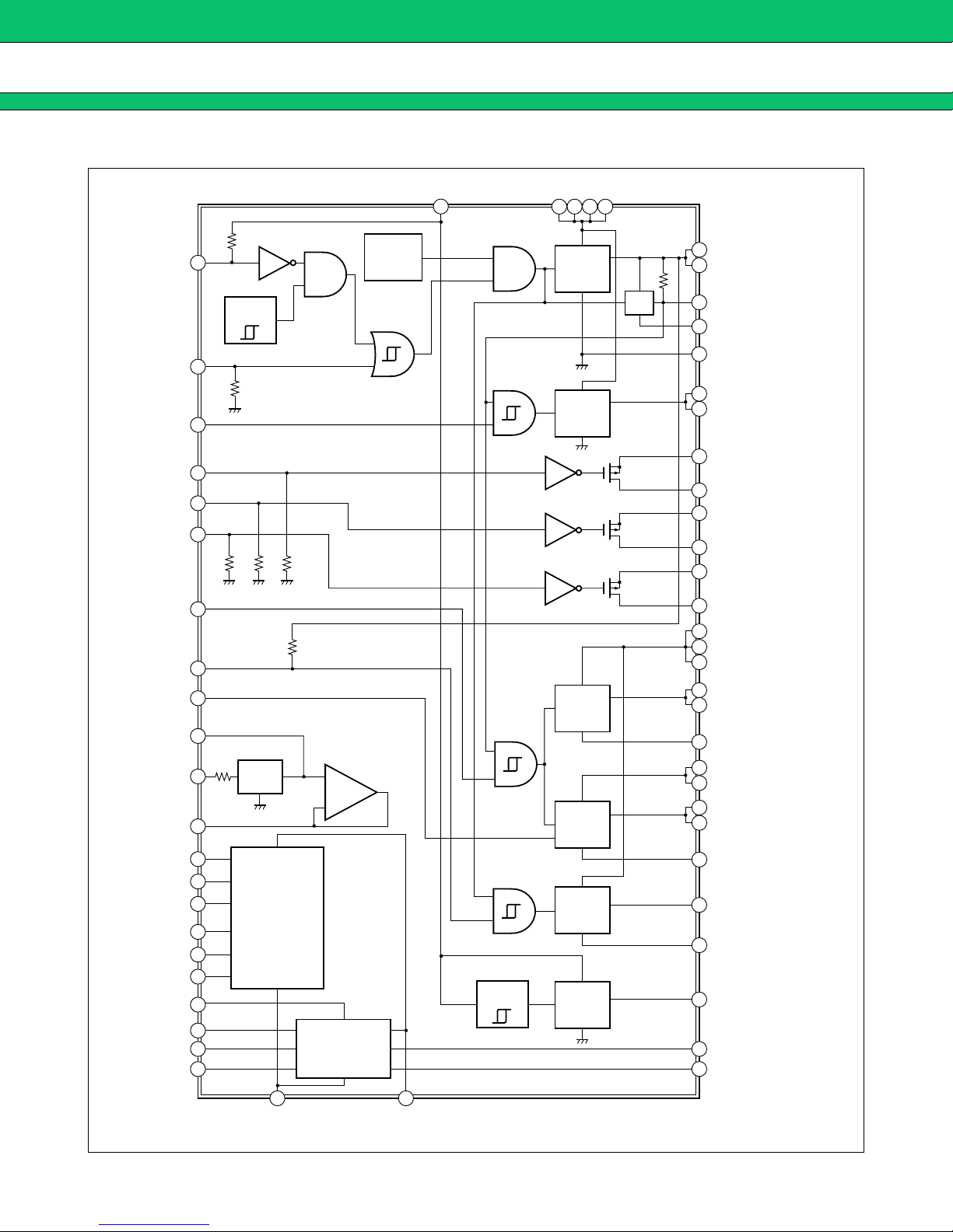
■BLOCK DIAGRAM
14
16
53
54
55
44
22
33
20 8 9 10 11
12
13
17
18
19
15
+
−
6
7
46
45
52
51
48
60
61
42
43
62
3
5
4
47
40
41
39
21
34
35
36
37
38
27
28
26
CONT1
CONT6
CONT2
SW1-ON
SW2-ON
SW3-ON
CONT4
VREF
RESET-IN
CLK-IN
µP-IO
RST
CLK
SIM-IO
VSIM-ON
SIMPROG
OSC
VBAT2 VBAT1
OUT1
OUT2
SW1-INPUT
SW1-OUTPUT
SW2-INPUT
SW2-OUTPUT
SW3-INPUT
SW3-OUTPUT
VBAT3
OUT3
GND3
VBAT4
OUT4
GND4
V-BACKUP
XPOWERGOOD
DELAYCAP
GND1
POR
Main
UVLO
Over
Temp
Protection
LDO1
LDO2
SW1
SW2
SW3
ON OUT
ON OUT
ON OUT
LDO3
ON OUT
LDO4
ON OUT
LDO5
ON OUT
LDO6
CONT4
BACKUP
UVLO
VREF VREF-AMP
GSM/SIM
Logic
Level
Translation
VSIMOUT
Charge-pump
57
CONT5
56
CONT3
31 VCAP−
30 VCAP+
59 GND5
58 OUT5
24
REF-OUT
23
VFIL
25
VCC-VSIM
29
VSIMOUT
32
GND-VSIM N.C.
Pin : 1, 2, 49, 50, 63, 64

MB3891
6
■
■■
■ABSOLUTE MAXIMUM RATINGS
* : The packages are mounted on the dual-sided epoxy board(10 cm ×10 cm)
WARNING: Semiconductor devices can be permanently damaged by application of stress (voltage, current,
temperature, etc.) in excess of absolute maximum ratings. Do not exceed these ratings.
■
■■
■RECOMMENDED OPERATING CONDITIONS
WARNING: The recommended operating conditions are required in order to ensure the normal operation of the
semiconductor device. All of the device’s electrical characteristics are warranted when the device is
operated within these ranges.
Always use semiconductor devices within their recommended operating condition ranges. Operation
outside these ranges may adversely affect reliability and could result in device failure.
No warranty is made with respect to uses, operating conditions, or combinations not represented on
the data sheet. Users considering application outside the listed conditions are advised to contact their
FUJITSU representatives beforehand.
Parameter Symbol Conditions Rating Unit
Min. Max.
Power supply voltage VBAT −0.3 7 V
VCC-VSIM −0.3 7 V
LDO regulator
IOOUT1 pin 120 mA
IOOUT2 pin 50 mA
IOOUT3 pin 100 mA
IOOUT4 pin 100 mA
IOOUT5 pin 50 mA
VSIMOUT chargepump IOVSIMOUT pin 10 mA
Power dissipation PDTa ≤+25 °C800* mW
Storage temperature Tstg −55 +125 °C
Parameter Symbol Conditions Value Unit
Min. Typ. Max.
Power supply voltage VBAT 3.0 3.6 5.5 V
VCC-VSIM 3.0 3.6 5.5 V
LDO capacitor guarantee value COOUT1 to OUT5, V-BACKUP pin 0.8 1.0 µF
REF-OUT capacitor guarantee
value COREF-OUT pin 0.027 µF
VSIMOUT capacitor guarantee
value COVSIMOUT pin 10 µF
Operating ambient temperature Ta −20 +25 +85 °C

MB3891
7
■
■■
■ELECTRICAL CHARACTERISTICS (Ta =+25 °C, VBAT1 to VBAT4 =VCC-VSIM =3.6 V)
* : Standard design value
(Continued)
Parameter Symbol Pin No. Conditions Value Unit
Min. Typ. Max.
General
Shutdown supply
current
IBAT1 8, 9, 10, 11,
20, 42, 43,
60, 61, 62
UVLO =“L”,
BACKUP UVLO =“L” 80 µA
IBAT2 8, 9, 10, 11,
20, 42, 43,
60, 61, 62
UVLO =“L”,
BACKUPUVLO=“H” 160 µA
Standby supply
current IBAT3 8, 9, 10, 11,
20, 42, 43,
60, 61, 62
All circuit’s = On
(No load) 400 µA
Operating ground
current IGND 4, 5, 19,
32, 59
All circuit’s -VSIM =
On Max. load on all
regulators 10 mA
UVLO threshold
voltage
VTHH 8, 9, 10, 11,
20, 42, 43,
60, 61, 62 OUT1 =ON 2.980 3.080 3.180 V
VTHL 8, 9, 10, 11,
20, 42, 43,
60, 61, 62 OUT1 =OFF 2.780 2.880 2.980 V
BACKUP UVLO
threshold voltage
VTHH 8, 9, 10, 11,
20, 42, 43,
60, 61, 62 V-BACKUP =ON 2.980 3.080 3.180 V
VTHL 8, 9, 10, 11,
20, 42, 43,
60, 61, 62 V-BACKUP =OFF 2.580 2.680 2.780 V
Input voltage
VIH 16, 56, 57 0.7 ×
OUT1 OUT1 V
VIL 16, 56, 57 00.3 ×
OUT1 V
VIH 14, 15, 44 0.7 ×
VBAT VBAT V
VIL 14, 15, 44 00.3 ×
VBAT V
VIH 26, 27 0.7 ×
VCC-VSIM VCC-VSIM V
VIL 26, 27 00.3 ×
VCC-VSIM V
Pull-up resistor RPU 17 15* kΩ
RPU 14, 57 200* kΩ
Pull-down resistor RPD 15,53,54,55 200* kΩ

MB3891
8
(Ta =+25 °C, VBAT1 to VBAT4 =VCC-VSIM =3.6 V)
(Continued)
Parameter Symbol Pin
No. Conditions Value Unit
Min. Typ. Max.
LDO1
(OUT1)
Output voltage VO12, 13 −50µA>OUT1>−120mA 2.000 2.100 2.200 V
Line regulation Line 12, 13 3.1 V < VBAT1 < 5.5 V 10 mV
Load reguration Load 12, 13 −50 µA>OUT1>−120mA 30 mV
Ripple rejection
∆VBAT1/∆OUT1 R.R 12, 13 f =217 Hz 45 dB
Dropout voltage VDO 12, 13 OUT1 =−120 mA 500 mV
GND current at low load IGND 19 OUT1 >−1 mA 30 µA
GND current at max. load IGND 19 OUT1 =−120 mA 2mA
Output noise volt. (RMS) VNOVL 12, 13 f =10 Hz to 1 MHz,
OUT1 =1 µF500 µV
XPOWER-
GOOD
(RESET)
Output voltage VOH 17 0.8 ×
OUT1 OUT1 V
VOL 17 00.1 ×
OUT1 V
Hold time TXPG 17 DELAYCAP =0.033 µF102540ms
LDO2
(OUT2)
Output voltage VO6, 7 −50 µA >OUT2 >−50 mA 2.700 2.800 2.900 V
Line regulation Line 6, 7 3.1 V < VBAT1 < 5.5 V 10 mV
Load regulation Load 6, 7 −50 µA >OUT2 >−50 mA 30 mV
Ripple rejection
∆VBAT1/∆OUT2 R.R 6, 7 f =217 Hz 45 dB
Dropout voltage VDO 6, 7 OUT2 =−50 mA 250 mV
GND current at low load IGND 19 OUT2 >−1 mA 30 µA
GND current at max. load IGND 19 OUT2 =−50 mA 1mA
Output noise volt. (RMS) VNOVL 6, 7 f =10 Hz to 1 MHz,
OUT2 =1 µF350 µV
General
purpose
switches Input/Output resistance
RSW1 45, 46 SW1-INPUT =2.8 V
(Gate/Source =2.8 V) 4.0 Ω
RSW2 51, 52 SW2-INPUT =2.8 V
(Gate/Source =2.8 V) 7.0 Ω
RSW3 47, 48 SW3-INPUT =2.8 V
(Gate/Source =2.8 V) 7.0 Ω

MB3891
9
(Ta =+25 °C, VBAT1 to VBAT4 =VCC-VSIM =3.6 V)
(Continued)
Parameter Symbol Pin No. Conditions Value Unit
Min. Typ. Max.
LDO3
(OUT3)
Output voltage VO3, 4 −50 µA >OUT3 >−100 mA 2.700 2.800 2.900 V
Line regulation Line 3, 4 3.1 V < VBAT3 < 5.5 V 10 mV
Load regulation Load 3, 4 −50 µA >OUT3 >−100 mA 30 mV
Ripple rejection
∆VBAT3/∆OUT3 R.R 3, 4 f =217 Hz 45 dB
Dropout voltage VDO 3, 4 OUT3 =−100 mA 250 mV
GND current at low load IGND 5OUT3>−1 mA 30 µA
GND current at max.
load IGND 5OUT3=−100 mA 2mA
Output noise volt. (RMS) VNOVL 3, 4 f =10 Hz to 1 MHz,
OUT3 =1 µF350 µV
LDO4
(OUT4)
Output voltage VO40, 41 −50µA>OUT4>−100mA,
CONT4 =“L” 2.700 2.800 2.900 V
VO40, 41 −50µA>OUT4>−100mA,
CONT4 =“H” 2.400 2.500 2.600 V
Line regulation Line 40, 41 3.1 V < VBAT4 < 5.5 V 10 mV
Load regulation Load 40, 41 −50 µA >OUT4 >−100 mA 30 mV
Ripple rejection
∆VBAT4 - OUT4/∆OUT4 R.R 40, 41 f =217 Hz 45 dB
Dropout voltage VDO 40, 41 OUT4 =−100 mA 250 mV
GND current at low load IGND 39 OUT4 >−1 mA 30 µA
GND current at max.
load IGND 39 OUT4 =−100 mA 2mA
Output noise volt. (RMS) VNOVL 40, 41 f =10 Hz to 1 MHz,
OUT4 =1 µF500 µV
LDO5
(OUT5)
Output voltage VO58 −50 µA >OUT5 >−50 mA 2.700 2.800 2.900 V
Line regulation Line 58 3.1 V < VBAT3 < 5.5 V 10 mV
Load regulation Load 58 −50 µA >OUT5 >−50 mA 30 mV
Ripple rejection
∆VBAT3/∆OUT5 R.R 58 f =217 Hz 45 dB
Dropout voltage VDO 58 OUT5 =−50 mA 250 mV
GND current at low load IGND 59 OUT5 >−500 µA20 µA
GND current at max.
load IGND 59 OUT5 =−50 mA 1mA
Output noise volt. (RMS) VNOVL 58 f =10 Hz to 1 MHz,
OUT5 =1 µF350 µV

MB3891
10
(Ta =+25 °C, VBAT1 to VBAT4 =VCC-VSIM =3.6 V)
(Continued)
Parameter Symbol Pin No. Conditions Value Unit
Min. Typ. Max.
LDO6
(V-BACKUP)
Output voltage VO21 −10 µA >V-BACKUP
>−250 µA2.000 2.100 2.200 V
Line regulation Line 21 3.1 V < VBAT2 < 5.5 V 10 mV
Load regulation Load 21 −10 µA >V-BACKUP
>−250 µA30 mV
Ripple rejection
∆VBAT2/
∆V-BACKUP R.R 21 f =217 Hz 25 dB
GND current at
low load IGND 19 V-BACKUP >−10 µA10 µA
GND current at
max. load IGND 19 V-BACKUP =−250 µA50 µA
Output noise volt.
(RMS) VNOVL 21 f =10 Hz to 1 MHz,
V-BACKUP =1 µF500 µV
Reverse current IRC 21 VBAT2 =0 V,
V-BACKUP =3.0 V 100 nA
REF-OUT
Output voltage VO24 0 µA >REF-OUT >−50 µA 1.200 1.225 1.250 V
Line regulation Line 24 3.1 V < VBAT2 < 5.5 V 10 mV
Load regulation Load 24 0 µA >REF-OUT >−50 µA 6mV
Ripple rejection
∆VBAT2/
∆REF-OUT R.R 24 f =217 Hz 50 dB
Output noise volt.
(RMS) VNOVL 24 f =10 Hz to 1 MHz,
REF-OUT =27 nF 250 µV
VSIMOUT
chargepump
Output voltage VO29 −50µA>VSIMOUT>−10mA,
SIMPROG =“H” 4.600 5.000 5.400 V
VO29 −50µA>VSIMOUT>−10mA,
SIMPROG =“L” 2.760 3.000 3.240 V
Line regulation Line 29 3.1 V < VCC-VSIM < 5.5 V 50 mV
Load regulation Load 29 −50 µA >VSIMOUT >−10 mA 100 mV

MB3891
11
(Ta =+25 °C, VBAT1 to VBAT4 =VCC-VSIM =3.6 V)
(Continued)
Parameter Symbol Pin No. Conditions Value Unit
Min. Typ. Max.
VSIMOUT
chargepump
Ripple rejection
∆VCC-VSIM/
∆VSIMOUT R.R 29 f =217 Hz 30 dB
Output current IO29 3.1V< VCC-VSIM< 5.5V,
VSIMOUT =5 V 10 mA
IO29 3.1V< VCC-VSIM< 5.5V,
VSIMOUT =3 V 6mA
GND current at
no load IGND 32 VSIMOUT >−50 µA100 µA
Efficiency at
max. load η25, 29 VSIMOUT =−10 mA,
VSIMOUT =5 V 85 %
Output ripple
voltage VRP 29 f =10 Hz to 1 MHz,
VSIMOUT =10 µF100 mVPP
Shutdown sup-
ply current ILDO 25 VSIM-ON =“L” 100 nA
GSM/SIM
logic level
translation
µp interface
Input voltage VIH 33, 34,
35 0.7 ×
OUT1 OUT1 V
VIL 33, 34,
35 00.3 ×
OUT1 V
Output voltage VOH 35 µP-IO (max.) =−20 µA0.8 ×
OUT1 OUT1 V
VOL 35 µP-IO (max.) =1 mA 0 0.2 ×
OUT1 V

MB3891
12
(Continued)
(Ta =+25 °C, VBAT1 to VBAT4 =VCC-VSIM =3.6 V)
Parameter Symbol Pin No. Conditions Value Unit
Min. Typ. Max.
SIM
interface
5 V
(SIMPROG
=H)
Output voltage VOH 36 RST (max.) =−20 µAVSIMOUT
−0.7 VSIMOUT V
VOL 36 RST (max.) =200 µA00.6 V
Rise time TR36 RESET-IN =RST =30 pF 400 µs
Fall time TF36 RESET-IN =RST =30 pF 400 µs
Output voltage VOH 37 CLK (max.) =−20 µA0.7 ×
VSIMOUT VSIMOUT V
VOL 37 CLK (max.) =200 µA00.5 V
Rise time TR37 CLK-IN =CLK =30 pF 27 ns
Fall time TF37 CLK-IN =CLK =30 pF 27 ns
Output voltage VOH 38 SIM-IO (max.) =−20 µA3.8 VSIMOUT V
VOL 38 SIM-IO (max.) =1 mA 0 0.4 V
Input voltage VIH 38 0.7 ×
VSIMOUT VSIMOUT V
VIL 38 00.8 V
Rise time TR38 SIM-IO =30 pF 1µs
Fall time TF38 SIM-IO =30 pF 1µs
SIM
interface
3 V
(SIMPROG
=L)
Output voltage VOH 36 RST (max.) =−20 µA0.8 ×
VSIMOUT VSIMOUT V
VOL 36 RST (max.) =200 µA00.2 ×
VSIMOUT V
Rise time TR36 RESET-IN =RST =30 pF 400 µs
Fall time TF36 RESET-IN =RST =30 pF 400 µs
Output voltage VOH 37 CLK (max.) =−20 µA0.7 ×
VSIMOUT VSIMOUT V
VOL 37 CLK (max.) =200 µA00.2 ×
VSIMOUT V
Rise time TR37 CLK-IN =CLK =30 pF 50 ns
Fall time TF37 CLK-IN =CLK =30 pF 50 ns
Output voltage VOH 38 SIM-IO (max.) =−20 µA0.7 ×
VSIMOUT VSIMOUT V
VOL 38 SIM-IO (max.) =1 mA 0 0.4 V
Input voltage VIH 38 0.7 ×
VSIMOUT VSIMOUT V
VIL 38 00.2 ×
VSIMOUT V
Rise time TR38 SIM-IO =30 pF 1µs
Fall time TF38 SIM-IO =30 pF 1µs

MB3891
13
■
■■
■TYPICAL CHARACTERISTICS
(Continued)
400
350
300
250
200
150
100
50
0012345
Ta =+25 °C
CONT1 =“L”
CONT2 =“H”
CONT3 =“H”
CONT4 =OPEN
CONT5 =OPEN
CONT6 =OPEN
VSIM-ON =“H”
SIMPROG =“H” OUT1 = No load
OUT2 = No load
OUT3 = No load
OUT4 = No load
OUT5 = No load
V-BACKUP = No load
VSIMOUT = No load
350
300
250
200
150
100
50
0012345
Ta =+25 °C
CONT1 =OPEN
CONT2 =“H”
CONT3 =“H”
CONT4 =OPEN
CONT5 =OPEN
CONT6 =“H”
VSIM-ON =“H”
SIMPROG =“H” OUT1 = No load
OUT2 = No load
OUT3 = No load
OUT4 = No load
OUT5 = No load
V-BACKUP = No load
VSIMOUT = No load
450
400
350
300
250
200
150
100
50
0
450
400
350
300
250
200
150
100
50
0
012345
Ta =+25 °C
CONT1 =OPEN
CONT2 =“H”
CONT3 =“H”
CONT4 =OPEN
CONT5 =OPEN
CONT6 =“H”
VSIM-ON =“H”
SIMPROG =“H” OUT1 = 18 Ω
OUT2 = 56 Ω
OUT3 = 28 Ω
OUT4 = 28 Ω
OUT5 = 56 Ω
V-BACKUP = 8.4 kΩ
VSIMOUT = 510 Ω
IBAT
IGND
3.0
2.5
2.0
1.5
1.0
0.5
0.0 01234567
Ta =+25 °C
OUT1 =1 µF
CONT1 =OPEN
CONT6 =“H”
3.0
2.5
2.0
1.5
1.0
0.5
0.0 012345
Ta =+25 °C
OUT1 =1 µF
CONT1 =“L”
CONT6 =OPEN
2.2
2.1
2.0
1.9
1.8
1.7 0−100 −200 −300 −500−400 −600 −700 −800
Ta =+25 °C
VBAT =3.6 V
CONT1 =“L”
CONT6 =OPEN
Power supply current IBAT (µA)
Power supply current vs. power supply voltage Power supply current vs. power supply voltage
Power supply voltage VBAT (V) Power supply voltage VBAT (V)
Output voltage vs. power supply voltage (LDO1)
Power supply current IBAT (mA)
Power supply voltage VBAT (V)
Output voltage VOUT1 (V)
Power supply current , GND current vs.
power supply voltage
Power supply voltage VBAT (V)
Output voltage VOUT1 (V)
Output voltage vs. load current (LDO1)
Load current ILOAD (mA)
GND current IGND (µA)
Output voltage VOUT1 (V)
Power supply voltage VBAT (V)
Output voltage vs. power supply
voltage (LDO1)

MB3891
14
0
−20
−40
−60
−80
−10010 100 1 k 10 k 100 k 1 M
Ta =+25 °C
VBAT =3.6 V
OUT1 =1 µF
OUT1 =18 Ω
CONT1 =“L”
CONT6 =OPEN
0
−20
−40
−60
−80
−10010 100 1 k 10 k 100 k 1 M
Ta =+25 °C
VBAT =3.6 V
OUT1 =1 µF
CONT1 =“L”
CONT6 =OPEN
0.6
0.5
0.4
0.3
0.2
0.1
0.0 0−50 −100 −150 −200
VBAT = 2.1 V
CONT1 = OPEN
CONT6 = “H” Ta =+85 °C
Ta =−20 °C
Ta =+25 °C
2.13
2.12
2.11
2.10
2.09
2.08−40 −20 0 20 40 60 80 100
VBAT = 3.6 V
CONT1 = OPEN
CONT6 = “H”
10
5
0
2.0
1.5
1.0
0.5
0.0
0.0 0.5 1.0 1.5 2.0 2.5 3.0 3.5 4.0 4.5 5.0
OUT1
VBAT
Ta = +25°C
OUT1 = 18 Ω
CONT1 = “L”
CONT6 = OPEN
Ripple rejection vs. frequency (LDO1) Ripple rejection vs. frequency (LDO1)
Ripple rejection R.R (dBm)
Frequency f (Hz) Frequency f (Hz)
Dropout voltage vs. load current (LDO1)
Dropout voltage VDO (V)
Load current ILOAD (mA)
Output voltage vs. ambient temperature (LDO1)
Output voltage VOUT1 (V)
Ambient temperature Ta ( °C)
Output voltage rising waveforms (LDO1)
Power supply voltage VBAT
t (ms)
Output voltage VOUT1 (V)

MB3891
15
(Continued)
4
3
2
1
02
1
0
0 50 100 150 200 250 300 350 400 450 500
Ta = +25°C
OUT1 = No load
CONT1 = “L”
CONT6 = OPEN
VBAT
OUT1
4
2
0
2
1
0
0.0 0.2 0.4 0.6 0.8 1.0 1.2 1.4 1.6 1.8 2.0
OUT1
VBAT
Ta = +25°C
VBAT = 1 µF
OUT1 = No load
CONT1 = “L”
CONT6 = OPEN
4
2
0
2
1
0
02040
60 80 100 120 140 160 180 200
OUT1
CONT1
Ta = +25°C
VBAT = 3.6 V
OUT1 = 18 Ω
CONT6 = OPEN
10
5
0
2.0
1.5
1.0
0.5
0.0
020 40 60 80 100 120 140 160 180 200
CONT1
OUT1
Ta = +25°C
VBAT = 3.6 V
OUT1 = No load
CONT6 = OPEN
2.0
1.5
1.0
0.5
0.0
2
1
0
0102030
40 50 60 70 80 90 100
OUT1
VC
OUT1 = 0 A −120 mA
Ta = +25°C
VBAT = 3.6 V
CONT1 = “L”
CONT6 = OPEN
VBAT = 3.6 V
VREF = 1.225 V LDO1 OUT1
1 µF
120 mA
4 V
0 V
VC
Output voltage falling waveforms (LDO1) Output voltage falling waveforms (LDO1)
Waveform at rapid change of output load
(LDO1)
Output voltage VOUT1 (V)
t (µs)
NPN collector voltage VC(V)
PowersupplyvoltageVBAT (V)
t (ms)
Output voltage VOUT1 (V)
t (s)
Output voltage rising waveforms (LDO1)
InputvoltageVCONT1 (V)
t (µs)
Output voltage VOUT1 (V)
Output voltage falling waveforms (LDO1)
t (ms)
[Measurement diagram]
(IC internal)
Power supply voltage VBAT (V)
Output voltage VOUT1 (V)
Input voltage VCONT1 (V)
Output voltage VOUT1 (V)

MB3891
16
(Continued)
2.0
1.5
1.0
0.5
0.0
2
1
0
0.0 0.5 1.0 1.5 2.0 2.5 3.0 3.5 4.0 4.5 5.0
OUT1 = −120 mA 0 A
VC
OUT1
Ta = +25°C
VBAT = 3.6 V
CONT1 = “L”
CONT6 = OPEN
VBAT = 3.6 V
VREF = 1.225 V LDO1 OUT1
1 µF
120 mA
4 V
0 V
VC
3.0
2.5
2.0
1.5
1.0
0.5
0.0
3
2
1
0
OUT2
VC
0 102030405060708090100
OUT2 = 0 A −50 mA
Ta = +25°C
VBAT = 3.6 V
CONT1 = “L”
CONT2 = “H”
CONT6 = OPEN
VBAT = 3.6 V
VREF = 1.225 V LDO2 OUT2
1 µF
50 mA
4 V
0 V
VC
3.0
2.5
2.0
1.5
1.0
0.5
0.0
3
2
1
0
0 102030405060708090100
OUT2
VC
OUT2 = −50 mA 0 A
Ta = +25°C
VBAT = 3.6 V
CONT1 = “L”
CONT2 = “H”
CONT6 = OPEN
VBAT = 3.6 V
VREF = 1.225 V LDO2 OUT2
1 µF
50 mA
4 V
0 V
VC
Waveform at rapid change of output load (LDO1)
Output voltage VOUT1 (V)
t (ms)
NPN Collector voltage VC(V)
[Measurement diagram]
(ICinternal)
Waveform at rapid change of output load (LDO2)
Output voltage VOUT2 (V)
t (µs)
NPN Collector voltage VC(V)
[Measurement diagram]
(IC internal)
Waveform at rapid change of output load (LDO2)
Output voltage VOUT2 (V)
t (ms)
NPN Collector voltage VC(V)
[Measurement diagram]
(IC internal)

MB3891
17
(Continued)
1.4
1.2
1.0
0.8
0.6
0.4
0.2
0.0 01234567
Ta =+25 °C
VFIL =0.1 µF
1.24
1.23
1.22
1.21
1.20
1.19−40 −20 0 20 40 60 80 100
VBAT =3.6 V
Ta =+25 °C
VBAT =3.6 V
VSIM-ON =“H”
SIMPROG =“H”
VSIMOUT =510 Ω
VSIMOUT =No load
100000
10000
1000
100
10
1012345
Ta =+25 °C
VBAT =3.6 V
VSIM-ON =“H”
SIMPROG =“L”
100000
10000
1000
100
10
1012345
VSIMOUT =510 Ω
VSIMOUT =No load
Ta =+25 °C
VBAT =3.6 V
VSIM-ON =“H”
SIMPROG = “H”
VSIMOUT = No load
SIMPROG = “L”
VSIMOUT = No load
5
4
3
2
1
001234567
Reference voltage VFIL (V)
Reference voltage vs. power supply voltage Reference voltage vs. ambient temperature
Power supply voltage VBAT (V) Ambient temperature Ta ( °C)
Output voltage vs. power supply voltage
(VSIMOUT Chargepump)
Power supply current ICC-VSIM (µA)
Power supply voltage VCC-VSIM (V)
Output voltage VSIMOUT (V)
Power supply current vs. power supply voltage
(VSIMOUT Chargepump)
Power supply voltage VCC-VSIM (V)
Power supply current ICC-VSIM (µA)
Power supply voltage VCC-VSIM (V)
Power supply current vs. power supply voltage
(VSIMOUT Chargepump)

MB3891
18
(Continued)
3.00
2.99
2.98
2.97
2.96
2.95
2.94
2.93
2.92
2.91
2.90 0−5−10 −15 −20
VCC-VISM =5.5 V
VCC-VISM =3.1 V VCC-VISM =3.6 V
Ta =+25 °C
VSIM-ON =“H”
SIMPROG =“L”
5.00
4.95
4.90
4.85
4.80
4.75
4.70
4.65
4.60 0−5−10 −15 −20
VCC-VISM =5.5 V
VCC-VISM =3.1 V VCC-VISM
=3.6 V
Ta =+25 °C
VSIM-ON =“H”
SIMPROG =“H”
0
−20
−40
−60
−80
−10010 100 1 k 10 k 100 k 1 M
Ta =+25 °C
VBAT =VCC-VSIM =3.6 V
VSIM-ON =“H”
SIMPROG =“H”
VCAP+VCAP−=0.1 µF
VSIMOUT =10 µF
VSIMOUT = 510 Ω
0
−20
−40
−60
−80
−10010 100 1 k 10 k 100 k 1 M
Ta =+25 °C
VBAT =VCC-VSIM =3.6 V
VSIM-ON =“H”
SIMPROG =“H”
VCAP+VCAP−=0.1 µF
VSIMOUT = 10 µF
0
−20
−40
−60
−80
−10010 100 1 k 10 k 100 k 1 M
Ta =+25 °C
VBAT =VCC-VSIM =3.6 V
VSIM-ON =“H”
SIMPROG =“L”
VCAP+VCAP−=0.1 µF
VSIMOUT =10 µF
VSIMOUT =510 Ω
0
−20
−30
−40
−80
−10010 100 1 k 10 k 100 k 1 M
Ta =+25 °C
VBAT =VCC-VSIM =3.6 V
VSIM-ON =“H”
SIMPROG =“L”
VCAP+VCAP−=0.1 µF
VSIMOUT =10 µF
Output voltage VSIMOUT (V)
Output voltage vs. load current
(VSIMOUT Chargepump) Output voltage vs. load current
(VSIMOUT Chargepump)
Load current ILOAD (mA) Load current ILOAD (mA)
Ripple rejection R.R (dBm)
Frequency f (Hz)
Ripple rejection vs. frequency
(VSIMOUT Chargepump)
Ripple rejection R.R (dBm)
Frequency f (Hz)
Ripple rejection vs. frequency
(VSIMOUT Chargepump)
Ripple rejection R.R (dBm)
Frequency f (Hz)
Ripple rejection vs. frequency
(VSIMOUT Chargepump)
Ripple rejection R.R (dBm)
Frequency f (Hz)
Ripple rejection vs. frequency
(VSIMOUT Chargepump)

MB3891
19
(Continued)
100
90
80
70
60
50
40
30
20
10
03.0 3.5 4.0 4.5 5.0 5.5
Ta =+25 °C
VSIM-ON =“H”
SIMPROG =“L”
ILOAD =−10 mA
ILOAD =−1 mA
100
90
80
70
60
50
40
30
20
10
03.0 3.5 4.0 4.5 5.0 5.5
ILOAD =−10 mA
ILOAD =−1 mA
Ta =+25 °C
VSIM-ON =“H”
SIMPROG =“H”
100
90
80
70
60
50
40
30
20
10
00−5−10 −15 −20
Ta =+25 °C
VBAT =VCC-VSIM =3.6 V
VSIM-ON =“H”
SIMPROG =“L”
VCC-VSIM =5.5 V
VCC-VSIM =3.6 V
VCC-VSIM =3.1 V
100
90
80
70
60
50
40
30
20
10
00−5−10 −15 −20
Ta =+25 °C
VBAT =VCC-VSIM =3.6 V
VSIM-ON =“H”
SIMPROG =“H”
VCC-VSIM =3.1 V
VCC-VSIM =3.6 V
VCC-VSIM =5.5 V
0.0 0.5 1.5 2.0 2.5 3.0 3.5 4.0 4.5 5.01.0
10
5
05
4
3
2
1
0
VSIM-ON
VSIMOUT
Ta =+25 °C
VBAT =VCC-VSIM =3.6 V
SIMPROG =“H”
VSIMOUT =510 Ω
0.0 0.5 1.5 2.0 2.5 3.0 3.5 4.0 4.5 5.01.0
10
5
0
3
2
1
0
VSIM-ON
VSIMOUT
Ta =+25 °C
VBAT =VCC-VSIM =3.6 V
SIMPROG =“L”
VSIMOUT =510 Ω
Efficiency η(%)
Efficiency η(%)
Efficiency vs. power supply voltage
(VSIMOUT Chargepump) Efficiency vs. power supply voltage
(VSIMOUT Chargepump)
Power supply voltage VCC-VSIM (V) Power supply voltage VCC-VSIM (V)
Efficiency η(%)
Load current ILOAD (mA)
Efficiency vs. load current
(VSIMOUT Chargepump)
Efficiency η(%)
Load current ILOAD (mA)
Efficiency vs. load current
(VSIMOUT Chargepump)
InputvoltageVSIM-ON (V)
t (ms)
Output voltage rising waveforms
(VSIMOUT Chargepump)
Output voltage VSIMOUT (V)
t (ms)
Output voltage rising waveforms
(VSIMOUT Chargepump)
Input voltage VSIM-ON (V)
Output voltage VSIMOUT (V)

MB3891
20
(Continued)
SIMPROG
VSIMOUT
Ta =+25 °C
VBAT =VCC-VSIM =3.6 V
VSIMOUT =510 Ω
VSIM-ON =“H”
0.0 0.5 1.5 2.0 2.5 3.0 3.5 4.0 4.5 5.01.0
10
5
05
4
3
2
1
0
SIMPROG
VSIMOUT
Ta =+25 °C
VBAT =VCC-SIM =3.6 V
VSIMOUT =510 Ω
VSIM-ON =“H”
0.0 0.5 1.5 2.0 2.5 3.0 3.5 4.0 4.5 5.01.0
10
5
05
4
3
2
1
0
0 5 15 20 25 30 35 40 45 5010
10
5
05
4
3
2
1
0
Ta =+25 °C
VBAT =VCC-VSIM =3.6 V
SIMPROG =“H”
VSIMOUT =510 Ω
VSIM-ON
VSIMOUT
0 5 15 20 25 30 35 40 45 5010
10
5
0
3
2
1
0
Ta =+25 °C
VBAT =VCC-VSIM =3.6 V
SIMPROG =“L”
VSIMOUT =510 Ω
VSIM-ON
VSIMOUT
0 2 6 8 10 12 14 16 18 204
40
20
0
−20
−40
Ta =+25 °C
VBAT =VCC-VSIM =3.6 V
VSIM-ON =“H”
SIMPROG =“H”
VSIMOUT =No load
AC COUPLED
0 2 6 8 10 12 14 16 18 204
20
0
−20
Ta =+25 °C
VBAT =VCC-SIM =3.6 V
VSIM-ON =“H”
SIMPROG =“L”
VSIMOUT =No load
AC COUPLED
Output voltage VSIMOUT (mV)
t (µs)
Output voltage waveforms
(VSIMOUT Chargepump)
Output voltage VSIMOUT (mV)
t (µs)
Output voltage waveforms
(VSIMOUT Chargepump)
Input voltage VSIMPROG (V)
t (ms)
Output voltage rising waveforms
(VSIMOUT Chargepump)
Output voltage VSIMOUT (V)
t (ms)
Output voltage falling waveforms
(VSIMOUT Chargepump)
Input voltage VSIM-ON (V)
t (ms)
Output voltage falling waveforms
(VSIMOUT Chargepump)
Output voltage VSIMOUT (V)
t (ms)
Output voltage falling waveforms
(VSIMOUT Chargepump)
Input voltage VSIMPROG (V)
Output voltage VSIMOUT (V)
Input voltage VSIM-ON (V)
Output voltage VSIMOUT (V)
Table of contents
Other Fujitsu Cell Phone Accessories manuals