Furuno FAX-30 User manual

FACSIMILE RECEIVER
FAX-30
Back

The paper used in this manual
is elemental chlorine free.
・FURUNO Authorized Distributor/Dealer
9-52 Ashihara-cho,
Nishinomiya, 662-8580, JAPAN
Telephone : +81-(0)798-65-2111
Fax : +81-(0)798-65-4200
A : NOV 2002
.
Printed in Japan
All rights reserved.
B3 : DEC . 15, 2010
Pub. No. SME-62600-B3
*
00080965100
*
*
00080965100
*
(KAOK ) FAX-30
*
00080965100
*
*
00080965100
*
* 0 0 0 8 0 9 6 5 1 0 0 *


Chapter 1 General ..................................................................................................1
Chapter 2 Circuit Description ..........................................................................2
Chapter 3 Location of Parts................................................................................9
Chapter 4 Maintenance
4.1 Self test ........................................................................................................................11
4.2 LED .............................................................................................................................12
4.3 Test Point.......................................................................................................................12
4.4 Adjustment ..................................................................................................................14
4.5 Jumper setting ..............................................................................................................14
4.6 DIP Switch setting.........................................................................................................14
4.7 Changing Program.........................................................................................................15
Content
s

This page is intentionally left blank.

Chapter 1 General
1
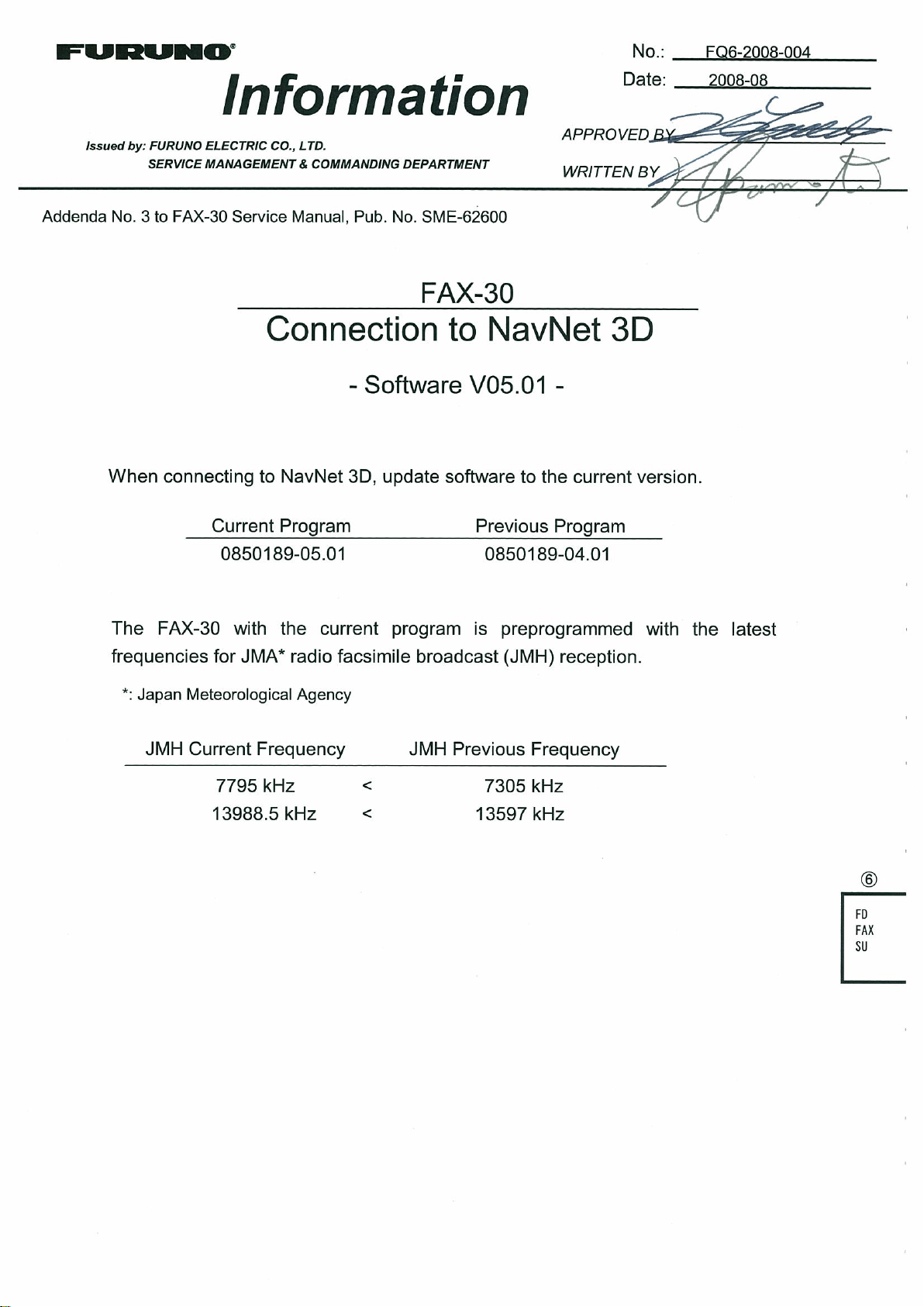
FAX-30 is a weather facsimile receiver. The received facsimile image is displayed on the
NavNet display unit and a PC.
1) NAVTEX function is not compliance with IMO standard. (For Non-SOLAS ship)
2) When FAX image is being received, NAVTEX message cannot be received.
3) The PC is required to run a web browser such as NETSCAPE or INTERNET EXPLORER.
4) Automatic station selection mode for NAVTEX reception requires position data from the
GPS.
5) When both the PC and NavNet are connected, FAX-30 is operated from the PC.
6) Receiving priority
(1) In FAX&NAVTEX mode, NAVTEX message is received except for the time set by
the timer.
(2) In FAX&NAVTEX mode, the priority is as follows.
FAX manual reception > FAX timer reception > NAVTEX reception
(3) The auto reception by receiving FAX start signal is valid only in FAX ONLY mode.

Chapter 2 Circuit Description
2
FAX-30 consists of MAIN, RCV and I/F boards.
Fig.1 Configuration of FAX-30
FAX-30
2.6 m whip antenna + FAX-5,
wire antenna or 6 m whip RCV board
NAVNET or PC
Power supply
12 VDC to 24 VDC
MJ6P connector
MJ3P connector
POWER LED
I/F
board MAIN board
M connector

Chapter 2 Circuit Description
3
MAIN board (08P3218)
MAIN board consists of CPU, NET and PWR circuits.
CPU circuit
CPU consists of 32-bit CPU&DSP with a built-in Ethernet controller, 24-bit CODEC (AD
converter), Flash ROM and SDRAM.
The main function of CPU&DSP (U18) is as follows.
1) Filtering of received signal (DSP)
2) Demodulation of FAX data (DSP)
3) Demodulation of NAVTEX data (DSP)
4) Communication with NAVNET or PC (CPU)
5) Processing position data for auto NAVTEX reception (CPU)
6) Setting the receiving frequency for RCV circuit (CPU)
FAX signal (16.29 kHz) and NAVTEX signal are AD-converted by the CODEC and sent to
CPU&DSP. Flash ROM memorizes the system program and the image for backup. SDRAM
memorizes FAX image.
Fig.2 Block Diagram of CPU Circuit
or
(Using
16 bit)

Chapter 2 Circuit Description
4
NET circuit
Net circuit is Ethernet 10Base-T interface circuit using TCP/IP protocol. U2 is a full feature
Physical Layer device with integrated PMD (Physical Medium Dependant) sublayers to support
10Base-T Ethernet protocol.
Fig.3 Block Diagram of NET Circuit
PWR circuit
Fig.4 shows the block diagram of power supply circuit. The power supply circuit employs a
floating type flyback switching regulator. Switching regulator controller U5 outputs a switching
signal of 190 kHz adjusted by R38. R51 adjusts +15 V line voltage.
Fig.4 Block Diagram of Power Supply Circuit
NAVNET or PC
10.8 VDC to 31.2 VDC
Controller
Protector
Reference
voltage
Reverse connection
protecting diode
Flyback
SW Poly switch
RT1
Filter
Rectifier
Feedback
+5 V
+3.3 V
+15 V
PULSE
TRANSFORMER
T1, T2

Chapter 2 Circuit Description
5
Power Supply Specification
Input voltage: 10.8 Vdc to 31.2 Vdc
Power consumption: 12 W (Maximum)
Input current: 1.0 A or less (12 V) and 0.5 A or less (24 V)
Protection circuit
PWR circuit is protected by;
Output short-circuit protector; 3.3 V line: U17 includes a protector.
5.0 V line: U16 includes a protector.
15 V line: poly switch, RT1
Input low- and over-voltage protector; U3 activates in the voltage range from 6.5 Vdc to
10.2 Vdc and from 32.8 Vdc to 40.5 Vdc.
Input reverse protector: Reverse protection diode, CR1
Input over-current protector; 2 A fuse blows out.
Signals between MAIN and RCV boards
MAIN and RCV boards are connected by following signal lines.
MAIN board
(PH14 pin) RCV board
(PH14 pin) Signal Name Remarks
#1 #1 0 V
#2 #2 0 V
#3 (output) #3 +15 V
#4 (output) #4 +15 V
#5 (output) #5 RCV DDS Strobe signal for DDS setting
#6 (output) #6 RCV PLL Strobe signal for PLL setting
#7 (output) #7 RCV CLK Clock receiving frequency setting
#8 (output) #8 RCV DATA Data receiving frequency setting
#9 (output) #9 RCV BAND Strobe signal for band selection
#10 (input) #10 RCV UNLOCK Synthesizer UNLOCK signal
#11 (output) #11 RCV TEST Self test signal
#12 (input) #12 AF_H
#13 (input) #13 AF_L FAX: 16290 Hz ± 400 Hz
NAVTEX: 16290 Hz ± 85 Hz
#14 #14 0 V

Chapter 2 Circuit Description
6
RCV board (08P3219)
Three bandpass filters, FL1, FL2 and FL3 locate at the first stage of the receiver. The filter
passes the following frequencies. When receiving NAVTEX message, FL3 is used.
FL1: 2 MHz to 13.2 MHz
FL2: 13.2 MHz to 25 MHz
FL3: 80 kHz to 518 kHz
The shift register, U10 receives three signals, RCV DATA, RCV CLK and RCV BAND from
MAIN board to select the filter. The signal passed through the filter is sent to the first mixer, Q5
and Q6.
The first mixer mixes RF signal with the first local oscillator signal, F+53.98371 MHz and
outputs the first IF signal, 53.98371 MHz. Further, the signal is mixed with the second local
oscillator signal, 54000 kHz at the second mixer, U4. The 16.29 kHz second IF signal is sent to
MAIN board.
Fig.5 Block Diagram of RCV Board

Chapter 2 Circuit Description
7
The synthesizer consists of 18 MHz oscillator, Direct Digital Synthesizer (DDS), PLL and VCO.
The signals from MAIN board, RCV DATA, RCV CLK, RCV DDS, RCV PLL and RCV BAND,
determines the frequency of the local oscillator depending on the selected receiving frequency.
When the synthesizer unlocks, RCV UNLOCK signal is generated for the error message.
The VCO is adjusted as follows.
Setting frequency Adjuster Voltage at TP4
29.9999 MHz T7 8.9 V to 9.1 V
25.5000 MHz No adjuster 5.3 V or more
25.4999 MHz No adjuster 8.0 V to 9.5 V
21.5000 MHz No adjuster 5.3 V or more
21.9999 MHz T6 8.9 V to 9.1 V
17.5000 MHz No adjuster 5.3 V or more
17.4999 MHz No adjuster 8.0 V to 9.5 V
13.5000 MHz No adjuster 5.3 V or more
13.4999 MHz T5 9.2 V to 9.4 V
9.5000 MHz No adjuster 5.3 V or more
9.4999 MHz No adjuster 8.0 V to 9.5 V
6.0000 MHz No adjuster 5.3 V or more
5.9999 MHz T4 8.9 V to 9.1 V
3.0000 MHz No adjuster 5.3 V or more
2.9999 MHz No adjuster 8.0 V to 9.5 V
0.0800 MHz No adjuster 5.3 V or more

Chapter 2 Circuit Description
8
CPU generates RCV TEST signal at the self test. Receiving this signal, the switch, Q11 turns on
and 18 MHz test signal is supplied to the antenna terminal.
Item Specification
Receiving frequency FAX LF: 80 kHz to 160 kHz
FAX MF/HF:2 MHz to 25 MHz
NAVTEX: 490 kHz/518 kHz
Emission mode FAX: F3C/J3C
(1) LF ± 150 Hz
Normal mode: white: +150 Hz; black: -150 Hz
Reverse mode: white: –150 Hz; black: +150 Hz
(2) MF/HF ± 400 Hz
Normal mode: white: +400 Hz; black: -400 Hz
Reverse mode: white: –400 Hz; black: +400 Hz
(3) NAVTEX: F1B (± 85 Hz FSK signal, 100 bps)
Antenna impedance 50 ohms
First IF signal 53.98371 MHz
Second IF signal 16.29 kHz
Synthesizer
Reference frequency: 18 MHz ± 2.5 ppm
First local oscillator: F+53.98371 MHz, 100 Hz step
Second local oscillator: 54000 kHz
Test signal: 18 MHz
Power supply to pre-amplifier +12 VDC
I/F board (08P3220)
3-pin, MJ connector for power supply and 6-pin, MJ connector for Network are soldered onto the
I/F board.

Chapter 3 Location of Parts
9
Fig.6 FAX-30, with cover removed
RCV board (08P3219) MAIN board (08P3218)
IF board
(08P3220)
LAN connector (Network)POWER connectorANT connector

Chapter 3 Location of Parts
10
Fig.7 RCV board (08P3219)
Fig.8 MAIN board (08P3218)
J23
(
ACT/WIRE
)
Filter 1, 2 and 3 TP5 (AGC)
R15
TP7
TP2
TP6 (+5V)
TP1 (0V) TP12 (0V)
TP13
(0V)
TP8 (2nd L0)
TP9 (AF)J22TP10 (18 MHz)VC0TP4 (VC0)TP3 (0V)TP11 (0V)J21
TP1 (SWF) TP2 R38 R51 TP7 (5V) J13 TP8 (15V) J12
TP9 (AF)J16
TP10 (0V)
TP11 (TEST)J15S1J17CR9 (G)
J11
J14 TP5 (0V)
TP6 (3.3V)
TP4 (CLK)
TP12 (0V)

Chapter 4 Maintenance
11
4.1 Self test
The self-test is performed by using the procedure below.
1. Press [MENU] on NavNet display.
2. Press “FAX-30 SYSTEMSETUP”.
3. Press “TEST” to start the test. The result appears as shown in Fig.9.
4. Press “RETURN” to return to the SYSTEM SETUP display.
Fig.9 Self test display
Table below lists the details of the test.
Item Description Item Description
ROM1 SS
Signal strength, 50 to 70
normally
ROM2
Flash ROM (U11) test. Test items are
differ between ROM1 and ROM 2. SN Signal to Noise ratio, 50 to 70
normally
SDRAM SDRAM test LAT/LON Latitude and longitude
RECEIVE
UNLOCK RCV board test
Displaying Detail Program version
The detail program version appears in the self test display when the unit is turned on with DIP
switch, S1, #2 on MAIN board set to ON position.
Example: 0850188-01.01
0850189-01.01
PROGRAM NO. 0850188-01
0850189-01
ROM1 OK
ROM2 OK
SDRAM OK
RECEIVER UNLOCK OK
SS 65
SN 60
LAT/LON OK

4.2 LED
12
4.2 LED
POWER LED (CR9, green) on MAIN board blinks as follows.
1) When loading the image at power-up; ON: 0.2 seconds, OFF: 0.2 seconds
2) At normal operation; ON: 1 second, OFF: 1 second
4.3 Test Point
The following signals appear at the test points.
MAIN board (08P3218)
TP No. Signal name Rating Remarks
TP1 SW F 190 kHz ± 5 kHz Switching frequency, Adjuster: R38
TP2 DC M DC minus
TP3 0 V
TP4 MCLK 29.655040 MHz ± 90 Hz GND: TP3
TP5 0 V
TP6 3.3 V 3.3 V ± 0.2 V
TP7 5 V 5 V ± 0.25 V
TP8 15 V 15.0 V ± 0.5 Adjuster: R51
Other manuals for FAX-30
5
Table of contents
Other Furuno Fax Machine manuals

Furuno
Furuno FAX-30 Owner's manual

Furuno
Furuno FAX-30 User manual

Furuno
Furuno FAX-30 User manual

Furuno
Furuno FAX-408 User manual

Furuno
Furuno FAX-207 User manual

Furuno
Furuno FAX-30 Manual

Furuno
Furuno DFAX FAX-208/A/N User manual

Furuno
Furuno FAX-207 User manual

Furuno
Furuno FAX-410 User manual

Furuno
Furuno DFax-208 How to use