GE LBI-31482 User manual

Mobile Communications
MAINTENANCE MANUAL
FOR
GENERAL ELECTRIC
33-50 MHz
BeaconMonitor Pager
Maintenance Manual
LBI-31482
Printed in U.S.A.

Copyright © June 1985, General Electric Company
TABLE OF CONTENTS
Page
DESCRIPTION . . . . . . . . . . . . . . . . . . . . . . . . . . . . . . . . . . . . . . . . . . . . . . . . . . . . . 2
OPERATION . . . . . . . . . . . . . . . . . . . . . . . . . . . . . . . . . . . . . . . . . . . . . . . . . . . . . . 2
BATTERY INFORMATION . . . . . . . . . . . . . . . . . . . . . . . . . . . . . . . . . . . . . . . . . . . . . . 2
CIRCUIT ANALYSIS . . . . . . . . . . . . . . . . . . . . . . . . . . . . . . . . . . . . . . . . . . . . . . . . . . 2
Receiver . . . . . . . . . . . . . . . . . . . . . . . . . . . . . . . . . . . . . . . . . . . . . . . . . . . . . . 2
Sequential Tone Decoder . . . . . . . . . . . . . . . . . . . . . . . . . . . . . . . . . . . . . . . . . . . . . 3
DETERMINATION OF TONE FREQUENCIES . . . . . . . . . . . . . . . . . . . . . . . . . . . . . . . . . . . 5
GE Format . . . . . . . . . . . . . . . . . . . . . . . . . . . . . . . . . . . . . . . . . . . . . . . . . . . . . 5
Quik-Call II Format . . . . . . . . . . . . . . . . . . . . . . . . . . . . . . . . . . . . . . . . . . . . . . . . 5
SERVICING
Disassembly . . . . . . . . . . . . . . . . . . . . . . . . . . . . . . . . . . . . . . . . . . . . . . . . . . . . 6
Alignment Procedure . . . . . . . . . . . . . . . . . . . . . . . . . . . . . . . . . . . . . . . . . . . . . . . 6
Troubleshooting . . . . . . . . . . . . . . . . . . . . . . . . . . . . . . . . . . . . . . . . . . . . . . . . . . 8
OUTLINE DIAGRAM . . . . . . . . . . . . . . . . . . . . . . . . . . . . . . . . . . . . . . . . . . . . . . . . . 11, 12
SCHEMATIC DIAGRAM . . . . . . . . . . . . . . . . . . . . . . . . . . . . . . . . . . . . . . . . . . . . . . . 13
PARTS LIST AND PRODUCTION CHANGES . . . . . . . . . . . . . . . . . . . . . . . . . . . . . . . . . . . . 14
PARTS BREAKDOWN . . . . . . . . . . . . . . . . . . . . . . . . . . . . . . . . . . . . . . . . . . . . . . . . . 15
TYPICAL SPECIFICATIONS
FCC Identification Number AXA9ERER-145-A1, B1, C1, D1
GE Type Number ER-145-A1: 41-45 MHz
ER-145-B1: 37-41 MHz
ER-145-C1: 33-37 MHz
ER-145-D1: 45-50 MHz
Frequency Range 33-50 MHz
Type of Operation Tone, Voice and Monitor
Signalling System Two-Tone Sequential
Audio Power Output (4 Ohm Speaker)
HI
LO 150 Milliwatts
20 Milliwatts
TYPICAL SPECIFICATIONS (CONT.)
Current Drain (at 2.5 Volts)
Standby
Receive 5.2 milliamperes
105 milliamperes
Battery Life
Nicke1-Cadmium
Mercury 25 hours
115 hours
Modulation Acceptance ±8 kHz
Channel Spacing 20 kHz
Selectivity (EIA) -65 dB
Paging Sensitivity 7 uV/meter
Usable Sensitivity (12 dB SINAD) 18 uV/meter
Spurious Response -56 dB
Frequency Stability ±5 PPM
Audio Distortion 5%
Dimensions (H x W x D) 110 x 52 x 36 millimeters (with belt clip)
(4.3 x 2 x 1.4 inches)
Weight 160 grams (5.66 ounces) with battery and belt clip
COMBINATION NOMENCLAURE
Digits 1 & 2
Digit 3
Digit 4 Digit 5 Digit 6 Digit 7 Digit 8
Product
Code
Tone
Option
Control Color Channel
Spacing Frequency
Range Distribution
L
T99/Quick Call
M
Separator W
Black 5
20 kHz B
33-37 MHz A
All Other
P8
Pager
R
Red C
37-41 MHz D
Dealer
D
41-45 MHz B
Less Xtals &
Reeds
E
45-50 MHz E
Less Xtals &
Reeds Dealer
LBI-31482 LBI-31482
1

DESCRIPTION
The General Electric BeaconMonitor Pager is a
highly reliable, extremely compact receiver for tone and
voice paging and channel monitor applications.
The Pager is equipped with a built-in speaker, earphone
jack and antenna, and is shipped with two nickel-cadmium
rechargeable batteries and an external earphone.
The receiver is housed in a ruggedly-constructed case,
with all operating controls conveniently mounted on the top
and side of the case. An accessory jack on the bottom of the
radio is provided for an external earphone.
Power for the Pager is normally supplied by two re-
chargeable nickel-cadmium batteries that fit in a separate
battery compartment in the bottom section of the case. The
batteries can be recharged either in or out of the receiver.
If desired, the Pager can also be operated by mercury,
zinc-carbon, or alkaline batteries. However, these batteries
are not rechargeable.
The spring clip on the Pager may be used to clip the ra-
dio to a pocket or belt.
OPERATION
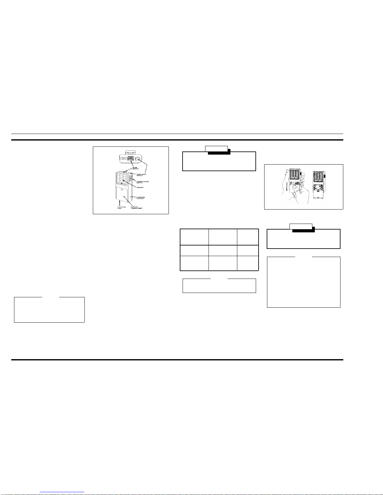
Turn the receiver on by placing the Power/Volume
switch to Volume HI position (See Figure 1). Several short
bursts of tone should be heard. The receiver is now ready to
receive messages.
Before a message is received, a short, interrupted burst
of tone will be heard, followed by a voice message. As soon
as the message is completed, press the Reset/Monitor button
to reset the receiver.
The Pager operates in either the SELECTIVE or MONI-
TOR mode.
In the SELECTIVE mode, the Pager operates as a tone
and voice receiver, and allows only those calls that are tone
coded for the Pager to be heard. After the call has been re-
ceived, the Pager switches automatically to the MONITOR
mode. The Pager will remain in the MONITOR mode, re-
ceiving all calls on the channel until the RESET switch is
pressed.
Placing the mode switch in the MONITOR position al-
lows all calls on the channel to be heard whether they are
tone coded or not. The Pager will squelch when no calls are
being received.
An earphone is available for use in high-noise areas, or
for receiving messages in private. Plugging the earphone
into the earphone jack disables the Pager speaker so that
messages can only be heard through the earphone.
After receiving the first message, it may be desirable to
reduce the volume by placing the OFF-HI switch in the LO
position.
CHARGERS
A single-unit desk-top charger and a multi-unit charger
are available for recharging the nickel-cadmium batteries in
the radio as well as spare nickel-cadmium batteries.
Temperature characteristics of nickel cadmium batteries
prevent a full charge at temperature extremes. For maxi-
mum capacity, recharge the batteries at room temperatures
between 65° to 85° Fahrenheit.
To use the charger, connect the power cable to an appropri-
ate power source. Place the Pager into the charger. The red
light will turn on, indicating that the Pager is being charged. To
charge spare nickel-cadmium batteries, place them into the bat-
tery insert. A second red light will come on to indicate that the
batteries are being charged.
BATTERY INFORMATION
Two different types of batteries are normally used in the
Pager.The type and battery life for each battery is shown in the
following chart.
BATTERY
TYPE PART
NUMBER TYPICAL
BATTERY
LIFE
Nickel-Cadmium
(Rechargeable) 19A703502P1 25 Hours
Mercury (Not
Rechargeable) 19A701300P1
Mallory MP401,
Eveready EP401E
115 Hours
BATTERYREPLACEMENT
The Pager is shipped from the factory ready for immediate
operation upon installation of two fully charged batteries.
To install or replace the batteries:
1. Slide the Pager OFF-HI switch to the OFF position.
2. Press in the battery cover on the ridges at the top of
the cover and slide cover down as shown.
3. Replace batteries according to the (+) and (-) signs in
the battery compartment.
4. Slide battery cover back into place.
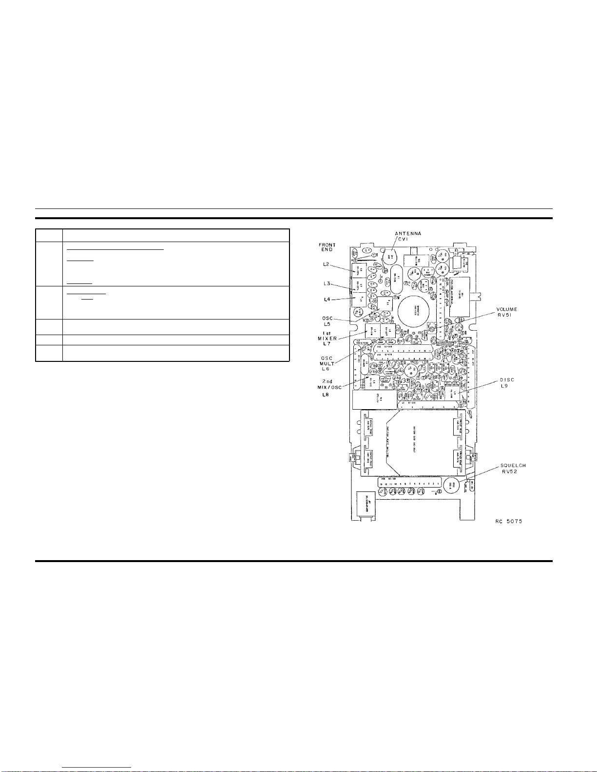
CIRCUITANALYSIS
RECEIVER
Paging receiver Types ER-145-A1, -B1, -C1 and -D1 are
double-conversion, superheterodyne receiver for tone and
voice paging in the 33-50 MHz range. One circuit board con-
Failure to press the Reset button after receiving a
message may shorten battery life. Do not press the
Reset button while receiving a message or an alert
tone. Doing so will prevent you from receiving the
message.
NOTE
Figure 1 - Operating Controls
Do not attempt to charge mercury, alkaline or zinc-
carbon batteries. To do so may cause the batteries to
explode.
WARNING
Nickel-cadmium batteries should be fully re-charged
before using.
NOTE
Do not dispose of either the rechargeable battery or the
Mercury battery by burning.To do so may cause abat-
tery to explode.
WARNING
There is no way to dispose of mercury batteries with-
out possible polution except by returning them to the
manufacturer for recycling.
Mallory Battery Company will buy all used mercury
batteries at the current market price. Batteries are to be
shipped prepaid, enclosing a packing slip indicating
who is to receive payment for the batteries to:
Mallory Battery Company
Plant #2
Lexington, North Carolina 27292
NOTE
Figure 2 - Battery Replacement
LBI-31482 LBI-31482
2

tains both tone and voice circuits, and utilizes both discrete
components and Thick Film Integrated Circuit Modules (IC’s).
The receiver has intermediate frequencies of 10.7 MHz and
455 kHz. Adjacent channel selectivity is provided by using
two, 2-pole ceramic filters. References to symbol numbers
mentioned in the following text are found in the Outline Dia-
gram, Schematic Diagram and Parts List (See Table of Con-
tents).A block diagram of the receiver is shown in Figure 3.
Receiver Front End
An RF signal from the antenna is coupled through the an-
tenna circuit to the base of RF amplifier Q1. The antenna cir-
cuit consists of L1, CV1 and C2. The circuit is tuned by CV1.
The output of Q1 is coupled through three tuned circuits
that provide most of the front end selectivity. The tuned cir-
cuits are L2, L3, L4 and associated circuitry. The output of L4
is coupled through C10 to the base of the first mixer.
1st Oscillator
Q2, X1, L5 and associated circuitry make up a Colpitts os-
cillator. The frequency is controlled by a third mode crystal op-
erated at one third of the required injection frequency. L5 is
used to set the oscillator on frequency. R3 is in parallel with
X1 to ensure operation on the third overtone of the crystal. The
injection frequency is the operating frequency (-) 10.7 MHz,
and is coupled through C16 to the first mixer. L6 is tuned to
three times, the crystal frequency. The output to the 1st mixer
is approximately 60-90 millivolts rms.
1st Mixer and IF Filter
RF from the Pager front end is applied to the base of first
mixer Q3. Injection voltage from the first oscillator is also ap-
plied to the base of Q3. The 10.7 MHz first IF frequency is
coupled through L7 to 10.7 MHz filter FL1. L7 is used to
match the mixer output to the input of FL1.
The highly-selective filter provides the first portion of the
receiver IF selectivity. The 10.7 MHz output of FL1 is applied
to the second mixer IC (Al).
2nd Oscillator, Mixer and IF Filter
Al and associated circuitry make up the 2nd oscillator and
mixer. The crystal for the oscillator is X2. The oscillator oper-
ates at 10.245 MHz for low side injection of the 2nd IF (stand-
ard), or 11.155 MHz for high side injection for those radios
determined to be operating on a tweet frequency. This fre-
quency is mixed with the 10.7 MHz input to provide the 455
kHz 2nd IF frequency.
The output of Al is coupled through ceramic filter FL2
which provides the 455 kHz selectivity. The filter output is ap-
plied to IF amplifier A2.
IFAmplifier and Detector
A2 and associated circuitry make up the IF amplifier. The
amplifier IC also provides the 455 kHz limiting. The output of
A2 is applied to the discriminator.
The discriminator demodulates the 455 kHz signal. This
type of detector provides a high degree of AM rejection. The
recovered audio, tone and noise is applied to audio amplifier
ICA51.
Audio Stages
The discriminator output is applied to buffer/pre-amp A51.
One output at A51-4 is coupled through high-pass filter A56
which filters out frequencies under 200 Hz to eliminate any
Channel Guard (CTCSS) tone. The filter output is applied to
squelch circuit A55, and to the decodercircuitry.
Applying the proper sequential tones to the receiver acti-
vates the decoder circuitry and audio stages, causing the sec-
ond alert tone to be heard at the speaker.
After the alert tone is heard, the output of A51 is applied to
the push-pull audio amplifiers Q51 and Q52, and then to the
speaker.
Squelch
Squelch control IC A55 monitors noise in the 30-40 kHz
range on A55-1. When there is no carrier present, the noise is
above a squelch threshold set by RV52. This condition makes
A55-7 high, shutting off the audio amp at A51-9. When a car-
rier is present, the noise level drops below the threshold driv-
ing A55-7 and A51-9 low. This turns the audio amp on
allowing transmissions on the channel to be monitored.
SEQUENTIAL TONE DECODER
The decoder is a two-reed, sequential tone decoder for op-
eration with any two-tone sequential encoder in individual call
applications.
The two reeds mount at the bottom of the circuit board, and
are available for operation on tone frequencies in the 288.5 to
2000 Hz range.
Figure 3 - Pager Block Diagram
LBI-31482 LBI-31482
3

The pager is also compatible with Quik-Call II two-tone
paging systems, and operates in both individual call and
group call applications.
Timing waveforms for the decoder circuitry are shown in
Figures 4-1, 4-2 and 5-1, 5-2. It is recommended that these
waveforms be studied in conjunction with the circuit analy-
sis for a better understanding of the decoder operation.
Tone Amplifiers & Reeds
When the proper tone sequence is applied to the Pager,
the discriminator output is applied to buffer/amplifier A51-1.
Tone A
When an HE signal containing Tone A is applied to the
Pager for approximately one second, the output at A51-2 is
applied to limiter-amplifier Q53. The square wave output of
Q53 drives reed FL51 into mechanical resonance. The reed
output is applied to tone amplifier Q54 which provides a
gain of approximately 20 dB. The amplifier output is recti-
fied by D52, and the resulting low (-0.2 VDC) is applied to
A52-1.
Tone B
After Tone A has been received, Tone B is applied to the
receiver for approximately three seconds. The tone is ampli-
fied by Q53 and applied to reed FL52. The reed output is
amplified by Q55 (approximately 20 dB gain) and rectified
by D53. The low output (-0.2 VDC) is applied to A53-1.
Individual Call
The one-second low output from Q54 and D52 applied to
A52-1 causes A52-6 to go low for approximately one second
after a delay of 0.6 second (See Figures 4-1 and 4-2). A52-6
then returns to a high state controlled by delay timer C68
and R69. The high at A52-6 causes A52-8 to go low momen-
tarily, and then go high.
After Tone A is received, Tone B causes a low to be ap-
plied to A53-1. The lows applied to A52-1 and A53-1 acti-
vate an “AND” gate in A52, causing the output at A52-11 to
go low for approximately 2.5 seconds. The low at A52-11 is
applied to A54-6, activating the alert tone oscillator.
The continuous tone output at A54-7 is shunted to ground
for 50 milliseconds at 100 millisecond intervals by Q59 to pro-
vide the interrupted alert tone. The alert tone is then applied to
A51-5.
The same time the tone alert oscillator starts, A55-5 and
A55-7 go low. The low at A55-7 is applied to amplifier A51-9,
turning the amplifier on so that messages can be heard.
GROUP CALL
In group call applications, only Tone B is applied to the re-
ceiver. The tone is applied for approximately 8 seconds. This
applies a low to A53-1, causing A53-6 to go low after a 0.3
second delay caused by C72. After a 5-second delay by delay
timer circuit R72, R73, and C73, A53-11 goes low and turns
off Q56. This allows Q57 to turn on, applying a low to A54-6
and a high to A54-3. This causes a continuous, interrupted 3.5
second alert tone to be heard, followed by the voice message.
ANTI-SHOCK CIRCUIT
When the Pager is subjected to a mechanical shock, both
reeds will vibrate and apply a low to pin 1 of A52 and A53.
This causes a high at pin 2 of decoders A52 and A53 which
disables the decoders to prevent falsing.
RESET/MONITOR CIRCUIT
Pressing momentary reset button S52 at any time applies a
negative pulse to A54-9. This drives A54-12 and squelch con-
trol IC A55-13 low. A55-7 then applies a low to audio amp
A51-9 and turns it on. While the reset button is depressed,
noise or any transmission on the Pager frequency will be
heard. Releasing the reset button causes A54-9, A54-12, A55-
13, A55-7 and A51-9 to all go high shutting off the audio amp
and resetting the Pager.
MODE SELECT
When mode select switch S53 is in the SEL (SELECT) po-
sition, A54-11 is high and the Pager operates in the tone and
voice paging mode. Placing S53 in the MON (MONITOR) po-
sition applies a low to A54-11, causing A54-6 to go low and
A54-12 to go high. This causes the Pager to switch to the
monitor mode so that all transmissions on the Pager frequency
can be monitored.
Figure 4-1 - Individual Call Timing Diagram Figure 4-2 - Individual Call Timing Diagram Figure 5-1 - Group Call Timing Diagram Figure 5-2 - Group Call Timing Diagram
LBI-31482 LBI-31482
4

DETERMINATION OF TONE
FREQUENCIES
The Pager can receive and decode two-tone sequential sig-
nals coded in the GE Type 99 format or the Motorola format.
The GE tone frequencies range from 517.5 Hz to 967.5 Hz.
Motorola tone frequencies range from 288.5 Hz to 1433.4 Hz.
The Pager is capable of both Individual and Group Call.
However, the Group Call will operate only with the Quik-Call
II signaling format.
GE FORMAT
INDIVIDUAL CALL
Tables 1 and 2 enable the technician to determine the tone
frequencies without opening the radio to examine the reed net-
works.
For example, assume the paging number to be 123. The
first digit of the paging number is a 1. Look in Table 1, and
read down the column labeled “100’s Digit” to a 1. Read hori-
zontally across to the column labeled “10’s Digit”. The tone
group is B. The second digit of the paging number is a 2. The
tone number is B2. Look in Table 2 and down the column la-
beled “Tone Designator” to find B2. Read horizontally across
to the column labeled “Tone Frequency”. The first tone fre-
quency is 787.5 Hz.
To determine the second tone frequency look in Table 1 and
as before, find the first digit of the paging number 1. Read
horizontally across to the column labeled “1’s Digit”.
The second tone group is A. The third digit of the paging
number is a 3 and the Tone Designator is A3. In Table 2 read
down the columnlabeled “Tone Designator” and find A3. Read
horizontally across the column labeled “Tone Frequency”. The
second tone frequency is 802.5 Hz.
For different paging numbers, locate the first digit in the
“100’s Digit” column and determine the tone frequencies as
described in the example. For a complete description of tone
applications see DATAFILE BULLETIN DF-5000-3A.
Table 1 - Tone Groups
100’S
DIGIT 10’S
DIGIT 1’S
DIGIT
For 1st
Tone For 2nd
Tone
0
1
2
3
4
5
6
7
8
9
A
B
B
A
C
C
C
A
B
Not Used
A
A
B
B
C
A
B
C
C
Table 2 - Tone Generator
TONE
GROUP TONE
DESIGNATOR TONE
FREQUENCY
A0
Al
A2
A3
A4
A5
A6
A7
A8
A9
682.5 Hz
592.5 Hz
757.5 Hz
802.5 Hz
847.5 Hz
892.5 Hz
937.5 Hz
547.5 Hz
727.5 Hz
637.5 Hz
B0
B1
B2
B3
B4
B5
B6
B7
B8
B9
652.5 Hz
607.5 Hz
787.5 Hz
832.5 Hz
877.5 Hz
922.5 Hz
967.5 Hz
517.5 Hz
562.5 Hz
697.5 Hz
C0
C1
C2
C3
C4
C5
C6
C7
C8
C9
667.5 Hz
712.5 Hz
772.5 Hz
817.5 Hz
862.5 Hz
907.5 Hz
952.5 Hz
532.5 Hz
577.5 Hz
622.5 Hz
Diagonal Tone 742.5 Hz
QUIK-CALL II FORMAT
INDIVIDUAL CALL
Tables 3 and 4 are used to determine the Quik-Call II
tone frequencies.
The first digit of the code determines the tone groups
used in the code (See Table 3). Then Table 4 is used to deter-
mine the actual tone frequencies.
Table 3 - Quik-Call II Code Numbers
FIRST DIGIT
OF
CODE
GROUP FROM
WHICH TONE A
IS SELECTED
GROUP FROM
WHICH TONE B
IS SELECTED
11 1
22 2
31 2
44 4
55 5
62 1
74 5
85 4
92 4
04 2
A3 3
For a code of 124, the tone groups used are shown in Ta-
ble 3. (Tone Aand Tone B are both located in Tone Group 1.)
Tone A is tone number 2 in Tone Group 1, and Tone B is
tone number 4. Refer to the following examples for addi-
tional information.
EXAMPLE 1 - Code 098:
The digit “0” in Table 3 (First Digit of Code) shows that
Tone A is in Tone Group 4, and Tone B is inTone Group
2 as shown in Table 4.
Tone number 9 in Tone Group 4 is 524.6 Hz.
Tone number 8 in Tone Group 2 is 879.0 Hz.
EXAMPLE 2 - Code 265:
The digit “2” in Table 3 shows that both Tone Aand Tone
B are both in Tone Group 2.
Tone number 6 is 788.5 Hz.
Tone number 5 is 746.8 Hz.
GROUP CALL
In Group Call application, the Tone Group is determined
by Table 5, while the frequency is determined by Table 4.
Refer to the following examples.
TONE
NO. TONE
GROUP 1 TONE
GROUP 2 TONE
GROUP 3 TONE
GROUP 4 TONE
GROUP 5 TONE
GROUP 6
1 349.0 Hz 600.9 Hz 288.5 Hz 339.6 Hz 584.8 Hz 1153.4 Hz
2 368.5 Hz 634.5 Hz 296.5 Hz 358.6 Hz 617.4 Hz 1185.2 Hz
3 389.0 Hz 669.9 Hz 304.7 Hz 378.6 Hz 651.9 Hz 1217.8 Hz
4 410.8 Hz 707.3 Hz 313.0 Hz 399.8 Hz 688.3 Hz 1251.4 Hz
5 433.7 Hz 746.8 Hz 953.7 Hz 422.1 Hz 726.8 Hz 1285.8 Hz
6 457.9 Hz 788.5 Hz 979.9 Hz 445.7 Hz 767.4 Hz 1321.2 Hz
7 483.5 Hz 832.5 Hz 1006.9 Hz 470.5 Hz 810.2 Hz 1357.6 Hz
8 510.5 Hz 879.0 Hz 1034.7 Hz 496.8 Hz 855.5 Hz 1395.0 Hz
9 539.0 Hz 928.1 Hz 1063.2 Hz 524.6 Hz 903.2 Hz 1433.4 Hz
0 330.5 Hz 569.1 Hz 1092.4 Hz 321.7 Hz 553.9 Hz 1122.5 Hz
Table 4 - Quik-Call II Tone Frequencies and Groups
Group Call code numbers range from 00 to 99. How-
ever, there are several Group Calls with the sameTone
B frequency. This limits the total number of Group
Calls to 40.
NOTE
LBI-31482 LBI-31482
5

EXAMPLE 1 - Group Call Code 07 (also code 27 and
37):
The digit “0” in Table 5 shows that Tone B is in Tone
Group 2 along with 20 to 29 and 30 to 39.Tone number 7 in
Tone Group 2 is 832.5 Hz (See Table 4).
EXAMPLE 2 - Group Call Code 98 (also code 48 and
88):
The digit “9” in Table 5 shows that Tone B is in Tone
Group 4 along with 40 to 49 and 80 to 89.Tone number 8 in
Tone Group 4 is 496.8 Hz.
Table 5 - Group Call Tone Groups (TG)
GROUP CALL
CODE NUMBER TONE GROUP
(Tone B)
00 - 09 TG2
10 - 19 TG1
20 - 29 TG2
30 - 39 TG2
40 - 49 G4
50 - 59 TG5
60 - 69 TG1
70 - 79 TG5
80 - 89 TG4
90 - 99 TG4
DISASSEMBLY
To gain access to the receiver board for servicing:
1. Loosen the two screws in the back cover and while
applying pressure to the lower portion of the front
cover, lift off cover.
2. With the speaker facing down, carefully loosen the
board in the front cover, starting with the bottom of
the printed board first.
3. Carefully turn the Pager over in the palm of the
hand (speaker facing up) and lift off the front
cover.
When replacing the board in the case, hold the case with
the speaker grill facing down and insert the Mode Select
switch, Reset switch and the Power/Volume switch into their
appropriate positions in the top of the case first. Make sure
the speaker is properly located. Then gently press the board
up into the case. Snap the back cover back into place and
tighten the two securing screws.
ALIGNMENT PROCEDURE
ALIGNMENT PROCEDURES
(33-50 MHz)
EQUIPMENT REQUIRED:
1. Multimeter.
2. SINAD Meter or Distortion Analyzer (with floating instrument circuit ground).
3. RF Signal Generator (two required).
4. 2-Tone Generator.
STEP PROCEDURE
1. Construct a 50 ohm coaxial cable (RG58-type) with a BNC connector on one end and clip leads on the other end.
2. Remove printed hoard assembly from case and insert fully charged batteries.
3. Connect the shield clip lead of the coaxial cable to the negative battery terminal. (This terminal connects directly
to chassis ground.)
4. Place the center conductor lead of the coaxial cable beneath the pager and lay pager flat on work bench. (cable
lead should be insulated from radio circuitry.)
5. Connect BNC end of cable to the RF Signal Generator.
6. Turn of the Pager and adjust squelch controlRV52 until the pager is fully un-squelched.
7. Set unmodulated RF signal generator to desired pager operating frequency. Keeping the RF generator exactly on
frequency. Slowly turn up the RF output of the generator until the pager starts to quiet.
8. Set another unmodulated RF generator to 10.7 MHz. Loosely couple this 10.7 MHz signal into coil form of L7.
9. Adjust L5 for desired frequency by tuning until a zero beat between the two signals is heard in the speaker.
10. Remove the 10.7 MHz signal. Connect an RF millivolt meter to TP1 and adjust L6 for maximum output on the
meter.
11. Modulate the RF generator with 1 kHz tone at 3 kHz deviation. Set the generator’s output so that an audible level
of approximately 12 dB SINAD is heard at the speaker.
12. Adjust L2, L3 and CV1 for best quieting. Reduce the generator output while tuning to maintain an audible level
of approximately 12 dB SINAD.
13. Adjust L7 to mid-range.
13.1 Connect the probe of the RF millivolt meter to TP1. Note thereading on the meter. Next, increase the radiated,
un-modulated RF input to the pager by turning up the generator output until a significant increase in meter
reading is obtained. Then adjust L4 for maximum reading on the meter. (If two peaks are observed, tune to the
one nearest the top of the coil form.)
Use short, direct cabling and wiring to keep RF interference to a minimum.
NOTE
LBI-31482 LBI-31482
6

RECEIVER ER-145-A1, B1, C1, D1
ISSUE 1
STEP PROCEDURE
14. Peform steps 14 and 15 Only if deemed necessary.
Discriminator: Apply a strong RF signal (approximately 1 mV Carrier with 1 kHz modulation at 3 kHz
deviation) and adjust the discriminator coil (L9) for maximum audio output level measured across the 4 ohm
speaker.
Service Note:If there are two output peaks, set the coil to the higher peak.
15. Audio Output Level: Apply a strong RF signal (approximately 1 millivolt carrier with 1 kHz modulation, but
now at 2 kHz deviation). Set the power/volume switch to HI, and adjust the audio gain potentiometer (RV51) for
rated audio output (150 milliwatts or 0.775 volts RMS across the 4-ohm speaker).
Set the Power/Volume switch to LO. The audio output level should drop 10 dB +2 dH.
16. Set up as in Step 11 above. Adjust squelch control (RV52) for an audible level of approximately 12 dB SINAD
squelch opening.
17. Slide S53 to SELposition and push S52 to reset pager.
18. Modulate the RF generator with the proper tone sequence from the 2-tone generator. Verify the alignment and
performance by successfully decoding several pages.
ALIGNMENT PROCEDURES
WITH TQ0602 TEST FIXTURE)
ALTERNATE TUNING PROCEDURE
1. Remove Printed Board Assembly from Case and insert fully charged batteries.
2. Place back cover of pager in fixture.
3. Place the pager on the cover.
4. Connect RF generator to RF input jack on fixture.
5. Go to step 6 of the main alignment procedure and continue through that procedure to complete the alignment.
LBI-31482 LBI-31482
7

RECEIVER ER-145-A1, B1, C1, D1
TROUBLESHOOTING PROCEDURE
LBI-31482 LBI-31482
8

RECEIVER ER-145-A1, B1, C1, D1
TROUBLESHOOTING PROCEDURE
LBI-31482 LBI-31482
9

RECEIVER ER-145-A1, B1, C1, D1
TROUBLESHOOTING PROCEDURE
LBI-31482 LBI-31482
10

SOLDER SIDE
ISSUE 1
OUTLINE DIAGRAM
LBI-31482 LBI-31482
11

COMPONENT SIDE
OUTLINE DIAGRAM
LBI-31482 LBI-31482
12

RECEIVER ER-145-A1, B1, C1, D1
SCHEMATIC DIAGRAM
LBI-31482 LBI-31482
13

PARTS LIST
33-50 MHz
BEACON MONITORPAGER
4DT-2049E
SYMBOL DESCRIPTION PART NO.
A1 Integrated Circuit 0800210000
A2 Integrated Circuit 0800200000
A51 Integrated Circuit 0800170000
A52 Integrated Circuit 0800180000
A53 Integrated Circuit 0800180000
A54 Integrated Circuit 0800190000
A55 Integrated Circuit 0801680000
A56 Integrated Circuit 0801690000
BT51 Nickel-Cadmium Battery 1.2V/150 mAh 5300170818
BT52 Nickel-Cadmium Battery 1.2V/150 mAh 5300170818
C1 — — — — —
C2 Ceramic Capacitor
30 MHz - 33 MHz 50V, RH200 pF 2004438321
33 MHz - 37 MHz 50V, RH160 pF 2004436321
37 MHz - 41 MHz 50V, RH100 pF 2004431321
41 MHz - 45 MHz 50V, RH75 pF 2004428321
45 MHz - 50 MHz 50V, RH51 pF 2004424321
C3 Ceramic Capacitor 50V, 2200 pF 2001901321
C4 Ceramic Capacitor 50V, 1000 pF 2001400321
C5 Ceramic Capacitor
30 MHz - 33 MHz 50V, RH43 pF 2004422321
33 MHz - 37 MHz 50V, RH36 pF 2004420321
37 MHz - 41 MHz 50V, SH27 pF 2001019321
41 MHz - 45 MHz 50V, SH24 pF 2001018321
45 MHz - 50 MHz 50V, SH20 pF 2001016321
C6 Ceramic Capacitor
30 MHz - 33 MHz 50V,CH4 pF 2001105321
33 MHz - 37 MHz 50V,CH4 pF 2001105321
37 MHz - 41 MHz 50V, CJ3 pF 2001104321
41 MHz - 45 MHz 50V, CJ3 pF 2001104321
45 MHz - 50 MHz 50V, CJ3 pF 2001104321
C7 Ceramic Capacitor
30 MHz - 33 MHz 50V, RH47 pF 2004423321
33 MHz - 37 MHz 50V, RH39 pF 2004421321
37 MHz - 41 MHz 50V, RH30 pF 2004418321
41 MHz - 45 MHz 50V, SH24 pF 2001018321
45 MHz - 50 MHz 50V, SH20 pF 2001016321
C8 Ceramic Capacitor
30 MHz - 33 MHz 50V, CJ3 pF 2001104321
33 MHz - 37 MHz 50V, CJ3 PF 2001104321
37 MHz - 41 MHz 50V, CK2 pF 2001103321
41 MHz - 45 MHz 50V, CK2 pF 2001103321
45 MHz - 50 MHz 50V, CK2 pF 2001103321
C9 Ceramic Capacitor
30 MHz - 33 MHz 50V, RH36 pF 2004420321
33 MHz - 37 MHz 50V, RH30 pF 2004418321
37 MHz - 41 MHz 50V, RH33 pF 2004419321
41 MHz - 45 MHz 50V, SH27 pF 2001019321
45 MHz - 50 MHz 50V, SH22 pF 2001017321
C10 Ceramic Capacitor 50V, 1000 pF 2001400321
C11 Ceramic Capacitor
33 MHz - 37 MHz 50V, SL47 pF 2001326321
37 MHz - 41 MHz 50V, SL47 pF 2001326321
41 MHz - 45 MHz 50V, SL47 pF 2001326321
45 MHz - 50 MHz 50V, SL47 pF 2001326321
C12 Ceramic Capacitor
33 MHz - 37 MHz 50V, SH33 pF 2001021321
37 MHz - 41 MHz 50V, SH33 pF 2001021321
41 MHz - 45 MHz 50V, SH22 pF 2001017321
45 MHz - 50 MHz 50V, SH22 pF 2001017321
C13 Ceramic Capacitor
33 MHz - 37 MHz 50V, SH33 pF 2001021321
37 MHz - 41 MHz 50V, SH33 pF 2001021321
41 MHz - 45 MHz 50V, SH22 pF 2001017321
45 MHz - 50 MHz 50V, SH22 pF 2001017321
C14 Ceramic Capacitor 50V, 1000 pF 2001400321
SYMBOL DESCRIPTION PART NO.
C15 Ceramic Capacitor
33 MHz - 37 MHz 50V, SH15 pF 2001013321
37 MHz - 41 MHz 50V, SH13 pF 2001012321
41 MHz - 45 MHz 50V, SH12 pF 2001011321
45 MHz - 50 MHz 50V, SH10 pF 2001009321
C16 Ceramic Capacitor
33 MHz - 37 MHz 50V,CH7 pF 2001108321
37 MHz - 41 MHz 50V,CH7 pF 2001108321
41 MHz - 45 MHz 50V,CH5 pF 2001106321
45 MHz - 50 MHz 50V,CH5 pF 2001106321
C17 Ceramic Capacitor 50V, 1000 pF 2001400321
C18 Tantalum Capacitor 4V, 10 uF 2013040501
C19 Tantalum Capacitor 4V, 10 uF 2013041501
C20 Ceramic Capacitor 50V, RH270 pF 2004441321
C21 Ceramic Capacitor 50V, RH270 pF 2004441321
C22 Ceramic Capacitor 50V, CH100 pF 2004135321
C23 Ceramic Capacitor 50V, 2200 pF 2001901321
C24 Ceramic Capacitor 50V, CJ3 pF 2001104321
C25 Chip Capacitor
33 MHz - 37 MHz 50V, CH39 pF 2004908061
37 MHz - 41 MHz 50V, CH33 pF 2004909061
41 MHz - 45 MHz 50V, CH22 pF 2004910061
45 MHz - 50 MHz 50V, CH15 pF 2004911061
C51 Tantalum Capacitor 35V, 0.01 uF 2014001501
C52 Tantalum Capacitor 35V, 0.1 uF 2014002501
C53 Tantalum Capacitor 35V, 0.22 uF 2014003501
C54 Tantalum Capacitor 4V, 100 uF 2013042501
C55 Tantalum Capacitor 4V, 100 uF 2013042501
C56 Tantalum Capacitor 4V, 100 uF 2013042501
C57 Tantalum Capacitor 35V, 0.1 uF 2013004501
C58 Tantalum Capacitor 10V, 1 uF 2014004501
C59 Ceramic Capacitor 50V, 1000 pF 2001400321
C60 Tantalum Capacitor 35V, 0.1 uF 2014002501
C61 Ceramic Capacitor 50V, 1000 pF 2001400321
C62 Tantalum Capacitor 10V, 1 uF 2014004501
C63 Tantalum Capacitor 10V, 1 uF 2014004501
C64 Ceramic Capacitor 50V, 330 pF 2001402321
C65 Ceramic Capacitor 50V, 1000 pF 2001400321
C66 Tantalum Capacitor 10V, 1 uF 2014004501
C67 Tantalum Capacitor 10V, 1 uF 2014004501
C68 Tantalum Capacitor 4V, 10 uF 2013040501
C69 Tantalum Capacitor 3V, 2.2 uF 2014005501
C70 Tantalum Capacitor 4V, 47 uF 2013041501
C71 Tantalum Capacitor 4V, 22 uF 2013043501
C72 Tantalum Capacitor 4V, 10 uF 2013040501
C73 Tantalum Capacitor 4V, 33 uF 2013044501
C74 — — — — —
C75 Tantalum Capacitor 10V, 1 uF 2014004501
C76 Tantalum Capacitor 3V, 2.2 uF 2014005501
C77 Tantalum Capacitor 16V, 0.68 uF 2014006501
C78 — — — — —
C79 Ceramic Capacitor 25V, 4700 pF 2001902321
C80 Tantalum Capacitor 35V, 0.022 uF 2014007501
C81 Tantalum Capacitor 4V, 22 uF 2013043501
C82 Aluminum Capacitor 4V, 47 uF 2029501803
C83 Ceramic Capacitor 50V, 1000 pF 2001400321
C84 Tantalum Capacitor 6.3V, 4.7 uF 2013032501
C85 Tantalum Capacitor 4V, 33 uF 2013044501
C86 Tantalum Capacitor 16V, 2.2 uF 2013023501
C87 Tantalum Capacitor 35V, 0.22 uF 2013005501
C88 Tantalum Capacitor 35V, 0.22 uF 2013005501
CV1 Variable Capacitor 250V, 40 pF 2090012803
D1 Diode 0500017501
D2 Diode 0500017501
D3 Diode 0500017501
D51 Diode 0500050324
D52 Diode 0500051324
D53 Diode 0500051324
D54 Diode, Varistor 0500028501
SYMBOL DESCRIPTION PART NO.
D55 Diode 0500052324
D56 Diode 0500050324
D57 Diode 0500051324
D58 Diode 0500017501
FL1 Ceramic Filter 10.7 MHz 5010011321
FL2 Ceramic Filter 455 kHz 501000532l
FL51 Reed Filter 5010002803
FL52 Reed Filter 5010002803
J51 Earphone Jack 2.5 ø 3700110718
J52 Filter Socket 3700130901
L1 Antenna Coil See Antenna (1)-(3)
L2 RF Coil 3002270101
L3 RF Coil 3002270101
L4 RF Coil
33 MHz - 37 MHz 3002270301
37 MHz - 41 MHz 3002270201
41 MHz - 45 MHz 3002270201
45 MHz - 50 MHz 3002270201
L5 RF Coil
33 MHz - 37 MHz 3002270501
37 MHz - 41 MHz 3002270401
41 MHz - 45 MHz 3002270401
45 MHz - 50 MHz 3002270401
L6 RF Coil 3002270601
L7 IF Coil 3001370401
L8 IF Coil 3001370501
L9 IF Coil 3001370501
Q1 Transistor (NPN) 0222232501
Q2 Transistor (NPN) 0235451501
Q3 Transistor (NPN) 0222232501
Q51 Transistor (PNP) 0009502324
Q52 Transistor (NPN) 0221202324
Q53 Transistor (NPN) 0226033806
Q54 Transistor (NPN) 0226033806
Q55 Transistor (NPN) 0226033806
Q56 Transistor (NPN) 0226033806
Q57 Transistor (NPN) 0226033806
Q58 Transistor (NPN) 0226033806
Q59 Transistor (NPN) 0226033806
Q60 Transistor (NPN) 0226033806
R1 Carbon Film Resistor 1/8 W, 33KΩ1001105803
R2 Carbon Film Resistor 1/8 W, 1KΩ1000070803
R3 Carbon Film Resistor 1/8 W, 1KΩ1001070803
R4 Carbon Film Resistor 1/8 W, 68KΩ1001112803
R5 Carbon Film Resistor 1/8 W, 1KΩ1001070803
R6 Carbon Film Resistor 1/8 W, 220Ω1001055803
R7 — — — — — — — — — —
R8 Carbon Film Resistor 1/8 W, 680Ω1001066803
R9 Carbon Film Resistor 1/8 W, 33KΩ1000105803
R10 Carbon Film Resistor 1/8 W, 22KΩ1001101803
R11 Carbon Film Resistor 1/8 W, 470Ω1001062803
R12 Carbon Film Resistor 1/8 W, 560Ω1001064803
SYMBOL DESCRIPTION PART NO.
R13 Carbon Film Resistor 1/8 W, 2.2KΩ1001078803
R14 Carbon Film Resistor 1/8 W, 680Ω1001066803
R15 Carbon Film Resistor 1/8 W, 100KΩ1001116803
R16 Carbon Film Resistor 1/8 W, 100KΩ1001116803
R51 Carbon Film Resistor 1/8 W, 100KΩ1001116803
R52 Carbon Film Resistor 1/8 W, 47KΩ1000108803
R53 Carbon Film Resistor 1/8 W, 220Ω1001055803
R54 Carbon Film Resistor 1/8 W, 10Ω1001024803
R55 DA Jumper — — — — —
R56 Carbon Film Resistor 1/8 W, 2.2MΩ1000346803
R57 Carbon Film Resistor 1/8 W, 100KΩ1001116803
R58 Chip Resistor 1/16 W, 100KΩ2004904061
R59 Carbon Film Resistor 1/8 W, 220KΩ1001124803
R60 Carbon Film Resistor 1/8 W, 1MΩ1001139803
R61 Carbon Film Resistor 1/8 W, 47KΩ1001108803
R62 Carbon Film Resistor 1/8 W, 220KΩ1001124803
R63 Chip Resistor 1/16 W, 100KΩ2004904061
R64 Carbon Film Resistor 1/8 W, 220KΩ1001124803
R65 Carbon Film Resistor 1/8 W, 1 MΩ1001139803
R66 Carbon Film Resistor 1/8 W, 47KΩ1001108803
R67 Carbon Film Resistor 1/8 W, 220KΩ1001124803
R68 Carbon Film Resistor 1/8 W, 18KΩ1001099803
R69 Carbon Film Resistor 1/8 W, 100KΩ1001116803
R70 Carbon Film Resistor 1/8 W, 100KΩ1001116803
R71 Carbon Film Resistor 1/8 W, 100KΩ1001116803
R72 Carbon Film Resistor 1/8 W, 47KΩ1001108803
R73 Carbon Film Resistor 1/8 W, 150KΩ1001120803
R74 Carbon Film Resistor 1/8 W, 56KΩ1001110803
R75 Carbon Film Resistor 1/8 W, 100KΩ1001116803
R76 Carbon Film Resistor 1/8 W, 39KΩ1001144803
R77 Carbon Film Resistor 1/8 W, 100KΩ1001116803
R78 Carbon Film Resistor 1/8 W, 100KΩ1001116803
R79 Carbon Film Resistor 1/8 W, 33KΩ1001105803
R80 Carbon Film Resistor 1/8 W, 220KΩ1001124803
R81 Carbon Film Resistor 1/8 W, 150KΩ1001120803
R82 Carbon Film Resistor 1/8 W, 10KΩ1001093803
R83 Carbon Film Resistor 1/8 W, 100KΩ1001116803
R84 Carbon Film Resistor 1/8 W, 47KΩ1001108803
R85 Carbon Film Resistor 1/8 W, 47KΩ1001108803
R86 Carbon Film Resistor 1/8 W, 100KΩ1001116803
R87 — — — — — — — — — —
R88 Carbon Film Resistor 1/8 W, 220KΩ1001124803
R89 Carbon Film Resistor 1/8 W, 10KΩ1001093803
RV51 Variable Resistor B-30KΩ1049022803
RV52 Variable Resistor B-22KΩ1049002004
S51 Slide Switch 4200001224
S52 Push Switch 4100001224
S53 Slide Switch 4200029004
SP51 Speaker 40ø 4Ω/0.1W 5210001370
X1 Crystal 4512403321
X2 Crystal 11.155 MHz 4506210221
or 10.245 MHz 4506209221
PARTS LIST
LBI-31482 LBI-31482
14

RECEIVER ER-145-A1, B1, C1, D1
Issue 1
MECHANICAL PARTS BREAKDOWN AND PARTS LIST
SYMBOL NO. DESCRIPTION GE STOCK NUMBER
1 FRONT CASE (BLACK) 2Mz-2111-1
FRONT CASE (RED) 2MZ-2111-2
2 PUSH BUTTON (1) 4MZ-1760-3
3 PUSH BUTTON (2) 4MZ-1761-3
4 SWITCH PARTS (1) 4MZ-2128-1
5 SWITCH PARTS (2) 4MZ-2129-1
6 SWITCH PLATE 4MZ-2114-1
7 SPEAKER NET 4MZ-1277
8 CUSHION 4MZ-0489-57
9 CHARGE CONTACT 4MB-7098-1
10 CHARGE CONTACT 4MB-7098-2
11 BATTERY COVER (BLACK) 3MZ-2113-1
BATTERY COVER (RED) 3MZ-2113-2
12 REAR COVER ASSEMBLY (BLACK) 2MZ-2112-1
REAR COVER ASSEMBLY (RED) 2MZ-2112-2
13 ANTI REMOVABLE SCREW 4MH-0634
14 ANTENNA CONTACT 4MB-6644
15 CLIP 3MZ-1894
16 NON. SLIDING PARTS 4MZ-1258
17 ANTENNA PLATE 4MB-6643
18 SPRING 4MB-5960
19 CLIP PIN 4MH-0829
20 BATTERY CASE 3MZ-2047
21 CONTACT 4MB-4287J
22 CONTACT POINT 4MB-7070
23 CUSHION 4MZ-2085
24 PARTITION PLATE 4MZ-2190
25 BATTERY CONTACT 4MB-7073
26 INSULATOR 4MZ-1936
27 ANTENNA CONTACT POINT 4MH-0841
28 TUNER CASE ASSEMBLY 4MB-5783
29 SUPPORT 4MZ-1333
30 INSULATOR 4MZ-2201
31 CUSHION 4MZ-19 71-1
32 CUSHION 4MZ-1971-2
33 CUSHION 4MZ-1971-3
34 NAMEPLATE 4MN-1770
35 SWITCH NAMEPLATE 4MN-2132
36 CALL SEAL 4MN-1771
37 SWITCH NAMEPLATE 4MN-1741
38 NUMBER SEAL 4MN-1883
39 DEALER LABEL 4MN-2088
40 FACTORY MUTUAL LABEL 4MN-2130
41 MAIN NAMEPLATE 3MN-1772
101 CYLINDER SCREW MI.7X5
LBI-31482 LBI-31482
15
Table of contents