GEKCO CLK100 Supplement

GEKCO
DIGITALCLOCK
MODELCLK100
ASSEMBLY&OPERATIONMANUAL
GEKCO Inc.
1565 SW Cypress Ln
McMinnville, OR 97128
(503) 472-4770 P/N595‐445REV1.1
Copyright 2021
GEKCO Inc.
All Rights Reserved
Printed in the United States of America
c

GEKCO DIGITAL CLOCK P/N CLK100 ASSEMBLY & OPERATION MANUAL
2 REV 1.1GEKCO INC.
THIS PAGE INTENTIONALLY BLANK

GEKCO DIGITAL CLOCK P/N CLK100 ASSEMBLY & OPERATION MANUAL
GEKCO INC. Rev 1.1 3
TABLE OF CONTENTS
1. INTRODUCTION ............................................................................................................................................... 5
2. OPERATIONAL SUMMARY .......................................................................................................................... 5
3. PARTS AND UNPACKING .............................................................................................................................. 6
3.1. TOP LEVEL PARTS LIST ...................................................................................................................................... 6
3.2. DISPLAY BOARD PARTS LIST ............................................................................................................................. 7
3.3. MAIN BOARD PARTS LIST .................................................................................................................................. 8
3.4. FINAL ASSEMBLY PARTS LIST ........................................................................................................................... 9
3.5. ENCLOSURE PARTS LIST ..................................................................................................................................... 9
4. ASSEMBLY NOTES......................................................................................................................................... 10
4.1. TOOLS ............................................................................................................................................................. 10
4.2. ASSEMBLY .................................................................................................................................................... 10
4.3. SOLDERING ................................................................................................................................................... 10
5. STEP-BY-STEP ASSEMBLY ......................................................................................................................... 11
5.1. DISPLAY CIRCUIT BOARD................................................................................................................................. 11
5.2. MAIN CIRCUIT BOARD ..................................................................................................................................... 15
6. INITIAL TESTS................................................................................................................................................. 17
7. FINAL TESTS .................................................................................................................................................... 18
8. IN CASE OF DIFFICULTY ............................................................................................................................ 18
9. FINAL ASSEMBLY .......................................................................................................................................... 18
10. OPERATIONAL INSTRUCTIONS .......................................................................................................... 21
10.1. SETTING THE TIME ............................................................................................................................................ 21
10.2. SETTING THE UTC MODE ON OR OFF ............................................................................................................. 21
10.3. SETTING THE UTC HOUR OFFSET.................................................................................................................... 21
10.4. SETTING THE ALARM TIME .............................................................................................................................. 22
10.5. SETTING THE ALARM ON OR OFF..................................................................................................................... 22
10.6. SETTING THE LOCAL TIME TO 12 OR 24 HOUR................................................................................................. 22
10.7. SETTING THE DISPLAY BRIGHTNESS ................................................................................................................ 22
11. THEORY OF OPERATION ....................................................................................................................... 24
11.1. BLOCK DIAGRAM.............................................................................................................................................. 24
11.2. MAIN BOARD CIRCUIT DESCRIPTION .............................................................................................................. 25
11.3. DISPLAY BOARD CIRCUIT DESCRIPTION.......................................................................................................... 25
12. FIRMWARE .................................................................................................................................................. 26
12.1. FLOW CHART .................................................................................................................................................... 26
12.2. FIRMWARE DESIGN DESCRIPTION.................................................................................................................... 26
12.2.1. Clock Mode.............................................................................................................................................. 26
13. PCA PICTORIAL DIAGRAMS ................................................................................................................. 27
13.1. MAIN BOARD .................................................................................................................................................... 27
13.2. DISPLAY BOARD ............................................................................................................................................... 28

GEKCO DIGITAL CLOCK P/N CLK100 ASSEMBLY & OPERATION MANUAL
4 REV 1.1GEKCO INC.
14. SCHEMATIC MAIN BOARD.................................................................................................................... 30
15. SCHEMATIC DISPLAY BOARD ............................................................................................................. 31
16. CUSTOMER SERVICE............................................................................................................................... 32
17. DOCUMENT REVISION HISTORY ....................................................................................................... 33
LIST OF FIGURES
FIGURE 1: DISPLAY BOARD TOP SIDE COMPLETED ASSEMBLY .................................................................................. 11
FIGURE 2: DISPLAY BOARD BOTTOM SIDE COMPLETED ASSEMBLY .......................................................................... 11
FIGURE 3DISPLAY BOARD BOTTOM SIDE .................................................................................................................... 12
FIGURE 4: DISPLAY BOARD TOP SIDE ASSEMBLY PICTORIAL ..................................................................................... 13
FIGURE 5: MAIN BOARD COMPLETED ASSEMBLY ....................................................................................................... 15
FIGURE 6MAIN BOARD TOP VIEW 1............................................................................................................................. 15
FIGURE 7: MAIN BOARD TOP VIEW 2 ........................................................................................................................... 15
FIGURE 8: MAIN BOARD TOP VIEW 3 ........................................................................................................................... 15
FIGURE 9: MAIN BOARD TOP VIEW 4 ........................................................................................................................... 16
FIGURE 10: MAIN BOARD BOTTOM VIEW .................................................................................................................... 16
FIGURE 11 RTC MODULE ASSEMBLY........................................................................................................................... 17
FIGURE 12: DISPLAY BOARD HARDWARE ASSEMBLY ................................................................................................. 18
FIGURE 13: DISPLAY BOARD TO MAIN BOARD ASSEMBLY ......................................................................................... 18
FIGURE 14: ENCLOSURE COVER TO BASE ASSEMBLY ................................................................................................. 19
FIGURE 15: FRONT PANEL ............................................................................................................................................. 19
FIGURE 16: FRONT PANEL TO BASE ASSEMBLY ........................................................................................................... 19
FIGURE 17: DISPLAY AND MAIN BOARD TO ENCLOSURE ASSEMBLY ......................................................................... 19
FIGURE 18 ENCLOSURE BACK ....................................................................................................................................... 20
FIGURE 19: MENU FLOW CHART................................................................................................................................... 23
FIGURE 20: BLOCK DIAGRAM ....................................................................................................................................... 24
FIGURE 21: SOFTWARE FLOWCHART ............................................................................................................................ 26
FIGURE 22: MAIN BOARD TOP ...................................................................................................................................... 27
FIGURE 23: MAIN BOARD BOTTOM .............................................................................................................................. 27
FIGURE 24 DISPLAY BOARD TOP SIDE .......................................................................................................................... 28
FIGURE 25 DISPLAY BOARD BOTTOM SIDE .................................................................................................................. 29

CLK100
GEKCO INC. Rev 1.1 5
1. Introduction
The Digital Clock Model CLK100 was designed to fill the need for an accurate digital clock with the
capabilities of two time zone displays in a compact format.
This clock has 6 digits for hours, minutes and seconds and the hours display can alternate between
two time zones, i.e. Coordinated Universal Time (UTC) and local time.
The CLK100 is offered in kit form or fully assembled and tested. The kit is easy to assemble with no
surface mount parts.
This step by step manual will guide you through the process to complete the assembly and testing of
the model CLK100 Digital Clock. The manual was designed so a total beginner in electronics can be
successful, but the more experienced builder can skip any unnecessary information. Also, this design
is fully open source for both the hardware and firmware. There are full schematics and pictorial
diagrams of the hardware, also there are links and flowcharts of the firmware microcontroller code.
2. Operational Summary
The Model CLK100 has 6 digits of seven segment displays to display HOURS, MINUTES and
SECONDS. The HOURS display can alternate between two time zones, which can be UTC and local
time. This function can be turned off by a menu selection if desired.
•The six digit display provides Hours, Minutes and Seconds
•Dual time zone display, alternates between two time zones every 2 seconds, i.e. UTC and
local
•The display LEDs are high contrast red, 0.56 inch character height
•Adjustable display brightness
•Local hours can be set for 12 or 24 hour mode
•Very accurate Real Time Clock (RTC) with battery backup
•Powered by a U.L. listed 5 VDC wall adapter
•Size: 4.16 x 2.35 x 3.5 inches (Width x Height x Depth)
•Weight: 0.75 pounds

GEKCO DIGITAL CLOCK P/N CLK100 ASSEMBLY & OPERATION MANUAL
6 REV 1.1GEKCO INC.
3. Parts and Unpacking
The kit is packaged in the order that the assembly is recommended. Each assembly block has an
associated parts bag. Only open a parts bag when called for during assembly to avoid misplacing parts.
3.1. Top Level Parts List
Remove the parts from the main bag and separate each individual parts bags.
ITEM
QTY
PART NO.
DESCRIPTION
1
1
DBR100-KIT
Clock Display Board PCA parts bag
2
1
CLK100M-KIT
Clock Main Board PCA parts bag
3
1
2217625
Real Time Clock (RTC) Module DS3231
4
1
CLK100HDW-KIT
Final Assembly Hardware
5
1
CLK100ENC-KIT
Enclosure with Front and Back Panels
6
1
54-660
AC to DC Power Supply Wall Adapter Single
Output 5 Volt 1 Amp 5 Watt 2.1mm Conn

DIGITAL CLOCK MODEL CLK100
GEKCO INC. Rev 1.1 7
3.2. Display Board Parts List
Clock 100 Display Board Printed Circuit Assembly (PCA) parts kit, P/N DBR100-KIT
ITEM
QTY
REFDES
PART NO.
DESCRIPTION
1
3
DS1,DS2,DS3
412-499
LED Display Module 7-Segment 2-Digit 0.56"
2
1
X1
434-3110
Socket IC Dip24-300
3
1
U1
442-3090
IC LED Display Driver MAX7219CNG
4
1
J1
131-1X10
Connector Header Single Row Male 10 pins
5
2
LED1,LED2
412-125
LED Red PCB Mount T1 3/4
6
1
C2
26-102
Cap elect alum radial lead 10uF/16v
7
1
C1
20-104
Cap mono Cer 50v radial lead
8
1
R1
6-1002-12
Res metal film 1/4w 1% 10k
9
1
81-180911D
PCB Display Board
1
2 3 8
6
5
7
4
3

GEKCO DIGITAL CLOCK P/N CLK100 ASSEMBLY & OPERATION MANUAL
8 REV 1.1GEKCO INC.
3.3. Main Board Parts List
Clock 100 Main Board PCA parts kit, CLK100M-KIT
ITEM
QTY
REFDES
PART NO.
DESCRIPTION
VALUE
1
3
C3,C4,C5
20-104
Cap mono Cer 50v radial lead
0.1UF
2
2
C1,C2
21-220
Cap mono Cer COG radial
lead
22pF 100v
3
1
C6
26-102
Cap elect alum radial lead
10uF/16v
4
1
Y1
404-160
Crystal HC49
16.00 MHz
5
1
D1
55-62
Diode schottky rectifier
1N5817-T
6
3
SW1,SW2,S
W3
64-1839
Switch Momentary SPST
7
1
SW4
64-1827
Switch Momentary 5mm H
8
1
J4
131-1X10S
Conn Header Female Single
Row 10 pins
9
1
J2
131-1X06RA
Conn Header Right Angle
Male 1 row of 6
pins
10
1
J3
131-1X05
Connector Header
Male 1 row of 5
pins
11
1
J1
134-002
Connector Power 2.1mm PCB
Mount
12
1
RN1
95-103
Res network 6 sip
10K 5 Res SIP
Package
13
1
X1
434-311
Socket IC
Dip28-300
14
1
U1
444-106-01
IC Microcontroller
Programmed
Part CLK100
V1.01
15
1
LS1
220-1420
Audio Piezo Transducer 30V
16
1
81-181004A
Printed Circuit Board
Main Board
1
2
16
3
4
5
6
7
13
14
8910
12
11
15

DIGITAL CLOCK MODEL CLK100
GEKCO INC. Rev 1.1 9
3.4. Final Assembly Parts List
Clock 100 Final Assembly Hardware parts kit, P/N CLK100HDW-KIT
ITEM
QTY
PART NO.
DESCRIPTION
1
2
258-616
Hardware Angle Bracket 4-40
2
2
250-1418
Hardware Screw Panhead 4-40 x 1/4”
3
2
250-1533
Hardware Screw Panhead 4-40 x 1/8”
4
2
252-440
Hardware Nut 4-40
3.5. Enclosure Parts List
Clock 100 Enclosure kit, P/N CLK100ENC-KIT
ITEM
QTY
PART NO.
DESCRIPTION
1
1
86-20113001
Enclosure Base
2
1
86-20113002
Enclosure Cover
3
2
86-20113003
Enclosure Bezel
4
1
86-181114F-A
Enclosure Front Panel
5
1
86-181114F-A
Enclosure Rear Panel
6
1
250-1410
Hardware Screw Flat-head 4-40 x 3/8”

GEKCO DIGITAL CLOCK P/N CLK100 ASSEMBLY & OPERATION MANUAL
10 REV 1.1GEKCO INC.
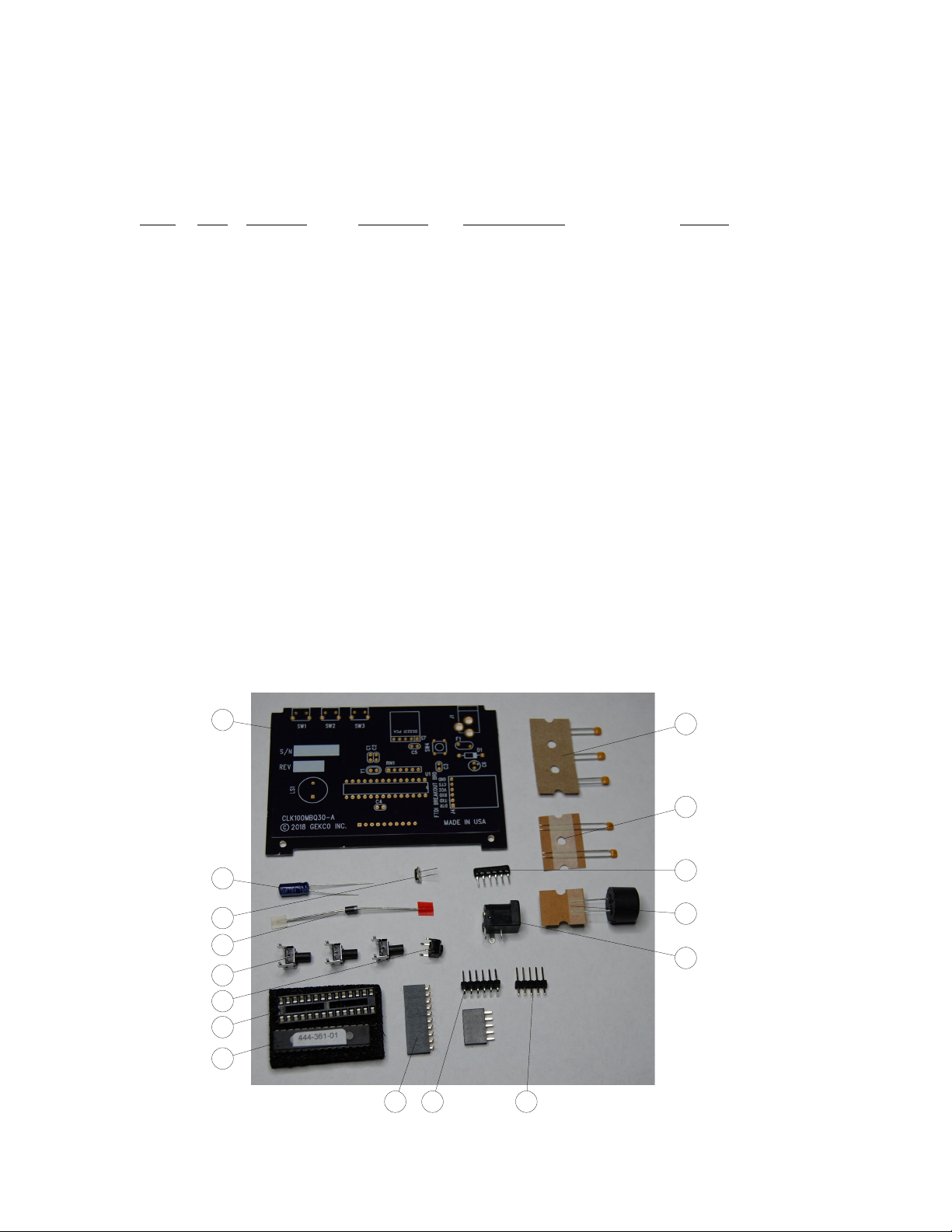
4. Assembly Notes
4.1. TOOLS
You will need these tools to assemble your kit.
•Diagonal Cutters
•Needle Nose Pliers
•Flat Head Screwdriver
•Philips Screwdriver (for the enclosure
only)
•Pencil Soldering Iron (22 to 25
WATTS)
4.2. ASSEMBLY
1. Follow the instructions carefully. Read the
entire step before you perform each
operation.
2. Refer to the Pictorial and Detail
Illustrations for help in performing the
assembly steps. The illustrations are
arranged in the proper sequence, as called
for in the assembly steps.
3. Pictorials show the overall operation for a
group of assembly steps: Details generally
illustrate a single step. When you are
directed to refer to a certain Pictorial “for
the following steps,” continue using that
Pictorial until you are referred to another
Pictorial for another group of steps.
4. Position all parts as shown in the
Pictorials.
5. Solder instructions are generally given only
at the end of a series of similar steps. You
may solder more often if you desire.
6. Each circuit part in an electronic kit has its
own reference designator (R3, C8, etc.).
Use these designators when you want to
identify the same part in the various
sections of the manual.
7. SAFETY WARNING: Avoid eye injury
when you cut off excessive lead
lengths. Wear safety glasses or
goggles and hold the leads so they
cannot fly toward your eyes.
4.3. SOLDERING
Soldering is one of the most important
operations you will perform while assembling
your kit. A good solder connection will form an
electrical connection between two parts such
as a component lead and a circuit board foil. A
bad solder connection could prevent an
otherwise well-assembled kit from operating
properly.
It is easy to make a good solder connection if
you follow a few simple rules:
Use the right type of soldering iron. A 22 to 25-
watt pencil soldering iron with a 1/8” or 3/16”
chisel or pyramid tip works best.
Keep the soldering iron tip clean. Wipe it often
on a wet sponge or cloth: then apply solder to
the tip to give the entire tip a wet look. This
process is called tinning, and it will protect the
tip and enable you to make good connections.
When solder tends to “ball” or does not stick to
the tip, the tip needs to be cleaned and re-
tinned.
NOTE: What solder to use, leaded or lead
free? The printed circuit boards in this kit are
plated with lead free solder so if you choose to
use lead free solder the complete assembly will
be RoHS compliant. Regarding kits though, it is
more difficult to solder with lead free material
due to the higher melting temperature, so we
recommend using a rosin core, radio-type
solder (60/40) or (63/37) tin-lead content) for all
of the soldering in this kit. If you decide to use
leaded solder, be careful to wash your hands
after soldering and never eat, drink or smoke,
until you wash thoroughly and you are done
soldering. Contain all materials that touched
leaded solder in a special container dedicated
for that purpose. This waste can be disposed
of at electronic-recycling events or contact your
waste management company

DIGITAL CLOCK MODEL CLK100
GEKCO INC. Rev 1.1 11
5. Step-By-Step Assembly
5.1. Display Circuit Board
Figure 1: Display Board Top Side Completed Assembly
Figure 2: Display Board Bottom Side Completed Assembly

GEKCO DIGITAL CLOCK P/N CLK100 ASSEMBLY & OPERATION MANUAL
12 REV 1.1GEKCO INC.
( ) Open the Display Board Printed Circuit Assembly (PCA) parts kit, P/N DBR656-KIT
Refer to Figure 3 for the following steps.
Position the Display Circuit Board with the bottom side facing up as shown
U3
NOTCH
Figure 3 Display Board Bottom Side
Locate the 24 pin IC socket for U3
Place the socket on the board with the notch on the socket aligned with the notch noted on the printed
circuit board (PCB) silkscreen. Turn the board over and solder the corner pins and check to be sure the
socket is firmly against the board and then solder the rest of the pins.
( ) X3: 24 pin DIP socket

DIGITAL CLOCK MODEL CLK100
GEKCO INC. Rev 1.1 13
Position the Display Circuit Board with the component side facing up as shown below
C1 R1 C2
Figure 4: Display Board Top Side Assembly Pictorial
Install the decoupling capacitor.
( ) C1: 0.1 uF (104) radial-lead ceramic capacitor
( ) R1: 10 kΩ(brn-blk-org-silver) resistor
NOTE: Before you install an electrolytic capacitor, look at it and identify the leads. One lead will have
either a negative ( −) mark or a positive ( +) mark near it on the side of the capacitor. The aluminum
electrolytic capacitor has the marking for a negative lead which may look like an oblong bar, sometimes
with a circle around it, inside an arrow. Be sure to install the positive lead in the positive-marked hole.
( ) C2: 10 uF radial-lead electrolytic aluminum capacitor (lay down the capacitor against the board
so it does not interfere with the enclosure)
C2 SIDE VIEW
( ) Solder the leads to the foil and cut off the excess lead lengths.
In the next step, make sure the LED display modules are oriented correctly. Match the decimal point on
the display with the orientation shown on the PCB silkscreen. Solder the corner pins first and make

GEKCO DIGITAL CLOCK P/N CLK100 ASSEMBLY & OPERATION MANUAL
14 REV 1.1GEKCO INC.
sure the display is mounted flush with the board and oriented correctly and then solder the rest of the
pins.
( ) DS1: 7 segment LED display module
( ) DS2: 7 segment LED display module
( ) DS3: 7 segment LED display module
Make sure the LEDs are oriented correctly, there is a flat side on the LED housing or make sure the
long lead (anode) is inserted in the square hole and the short lead (cathode) in the round hole.
( ) LED1: LED Red PCB Mount
() LED2: LED Red PCB Mount
Note: LED3, LED4, LED5 and LED6 are not installed in this version of the display board.
( ) Solder the leads to the foil and cut off the excess lead lengths.
This completes the assembly of the Display Board. Connector J1 will be installed after the main board
assembly is almost complete. Set aside for the final assembly later.

DIGITAL CLOCK MODEL CLK100
GEKCO INC. Rev 1.1 15
5.2. Main Circuit Board
Figure 5: Main Board Completed Assembly
Figure 6 Main Board Top View 1
() C3: 0.1 uF (104) radial-lead ceramic
capacitor
( ) C4: 0.1 uF (104) radial-lead ceramic
capacitor
( ) C5: 0.1 uF (104) radial-lead ceramic
capacitor
Figure 7: Main Board Top View 2
() C1: 22 pF (22) radial-lead ceramic
capacitor
( ) C2: 22 pF (22) radial-lead ceramic
capacitor
( ) C6: 10 uF radial-lead electrolytic
aluminum capacitor
Figure 8: Main Board Top View 3
() Y1: Crystal HC49 16 MHz
For the next step, be careful to position the end
with the dot or line towards the “square pad”
and tapered outline on the circuit board. After
you solder the first pin make sure the pins are
fully seated in their holes, solder the rest of the
pins to the foil.
( ) RN1: 10 kΩ103 resistor pack.
NOTE: When you install the diode, be sure to
orient the diode correctly. Always match the
band on the diode with the band mark on the

GEKCO DIGITAL CLOCK P/N CLK100 ASSEMBLY & OPERATION MANUAL
16 REV 1.1GEKCO INC.
circuit board. The circuit will not work properly if
a diode is installed backwards.
( ) D1: 1N5817 schottky diode
When installing the IC socket next, be sure to
align the notch on the socket with the notch on
the PCB silkscreen.
( ) X1: 28 pin DIP socket
Figure 9: Main Board Top View 4
() SW1: momentary right angle switch
( ) SW2: momentary right angle switch
( ) SW3: momentary right angle switch
( ) SW4: momentary switch
( ) J2: Connector Header Male 6 pin right
angle mount
( ) J3: Connector Header Male 5 pin right
angle mount
In the next step, solder one pin and re-align the
connector if necessary and then solder the rest
of the pins. The connector needs to be aligned
with the silkscreen outline.
( ) J1: Connector Power 2.1 mm
( ) LS1: Audio Piezo Speaker
( ) Solder the leads to the foil and cut off
the excess lead lengths.
The next step is to install the mating connector
between the display board (J1) and the main
board (J4). Turn the board over and install
connector J4 on the bottom side of the PCB.
Figure 10: Main Board Bottom View
This completes the assembly of the Main
board.
CIRCUIT BOARD CHECKOUT
Carefully inspect the circuit boards for the
following problems.
( ) Unsoldered connections
( ) Poor solder connections
( ) Solder bridges between foil patterns
( ) Protruding leads which could touch
together
Refer to the illustration where the parts were
installed as you make the following visual
checks.
( ) Diodes for the proper type and
positioning of the banded end
( ) Electrolytic capacitors for the correct
position of the positive ( +) or a negative ( −)
marked ends

DIGITAL CLOCK MODEL CLK100
GEKCO INC. Rev 1.1 17
() Locate the RTC module and install on
the clock main board as shown.
RTC Module
Figure 11 RTC Module Assembly
6. Initial Tests
Before installing the IC’s perform the following
tests.
Display Board
Using a multi-meter to measure resistance
perform the following checks.
( ) Verify that the resistance with the
positive lead on C1 positive pin and negative
lead on C1 negative pin, is greater than 2k
ohms.
Main Board
( ) Verify that the resistance with the
positive lead on D1 cathode ( the component
end with the band) and negative lead on the
ground pad TP1, is greater than 2k ohms.
IC INSTALLATION.
NOTE: You will install the following IC’s on the
main circuit board.
CAUTION: Integrated circuits (IC’s) are
complex electrical devices that perform many
complicated operations in a circuit. These
devices can be damaged during installation.
Read all of the following information before you
install the IC’s.
Some of the IC’s you will install in the following
steps are MOS {metal oxide semiconductor)
devices. Be sure they do not get damaged by
static electricity. Once you remove the IC from
the foam pad, do not let go of it or lay it down
until it is in its socket. Install it as follows. Read
all of the following steps before you pick up an
IC.
1. Pick up the IC and touch the foam pad
with both hands.
2. Hold the foam pad with one hand and
remove the IC with the other hand.
3. Continue to hold the IC with the one hand
and straighten any bent pins with the other
hand.
4. The pins on the IC’s may be bent out at an
angle as shown in A, and if this is the case,
they will not line up with the holes in the IC
socket or circuit board pads. Lay the IC
down on its side as shown in B and very
carefully roll it toward the pins to bend the
lower pins into line. Then turn the IC over
and bend the pins on the other side in the
same manner. Do not try to install and IC
without first bending the pins as described.
To do so may damage the IC pins or the
socket, causing an intermittent contact.
Install the IC on the display circuit board. Be
sure to line up the dimple with the circuit board
silkscreen
( ) U1: MAX7219 IC
Install the IC on the main circuit board:
( ) U1: ATMEGA328P IC
This completes the assembly of the circuit
boards.

GEKCO DIGITAL CLOCK P/N CLK100 ASSEMBLY & OPERATION MANUAL
18 REV 1.1GEKCO INC.
( ) Locate the miscellaneous hardware bag
and attach the angle bracket to the display
board using the 4-40 screws and nuts as
shown.
Figure 12: Display Board Hardware Assembly
( ) Attach the display board assembly to the
main board using the two 4-40 x 1/8” screws.
Figure 13: Display Board to Main Board Assembly
This completes the final assembly of the main
and display boards
7. Final Tests
Using a multi-meter to measure resistance
perform the following checks.
( ) Verify that the resistance with the
positive lead on U5 pin 20 and negative lead
on pin 10, is greater than 2k ohms.
( ) Connect the plug in transformer T1 to
power connector PS1 and plug into a wall
outlet and verify that the voltage with the
positive lead on U5 pin 20 and negative lead
on pin 10, is 5V.
8. In Case Of Difficulty
The “Visual Checks” that are provided below
will help you locate any difficulties that might
occur during the assembly and testing of your
Digital Clock. Additional “ In Case of Difficulty”
information is also provided in your Operation
Manual.
In an extreme case where you are unable to
resolve a difficulty, refer to the “Customer
Service” information at the back of the Manual.
VISUAL CHECKS
1. The majority of kits that fail are due to poor
solder connections. Therefore, you can
eliminate many difficulties by carefully
inspecting each connection to make sure it
is soldered as described in the solder
instructions section. Reheat any doubtful
connections.
2. Check the circuit board to be sure there
are no solder bridges between adjacent
connections.
3. Check capacitor values carefully. Be sure
the proper value part is installed at each
capacitor location and that the negative
( −) mark or a positive ( +) mark is
oriented correctly.
4. Check each resistor value carefully.
5. Be sure the correct diode is installed at
each location, and that the banded end is
positioned correctly.
6. Check the orientation and the correct part
number of the Integrated Circuits. Use the
pictorial diagrams as a reference.
9. Final Assembly
Skip these steps if the enclosure is not used.

DIGITAL CLOCK MODEL CLK100
GEKCO INC. Rev 1.1 19
( ) Unpack the enclosure parts kit, which
includes the front and back panels with bezels,
four 4-40 flat head screws and the base and
cover pieces.
( ) Slide the cover into the base as shown
in figure 14.
Figure 14: Enclosure Cover to Base Assembly
( ) Insert the front panel into one of the
bezels and attach to the enclosure front end as
shown in figure 15.
Figure 15: Front Panel
( ) Attach the front panel with the bezel to
the enclosure base with two 4-40 pan head
screws.
Figure 16: Front Panel to Base Assembly
( ) Slide the main and display board
assembly into the enclosure base from the
back end as shown.
Figure 17: Display and Main Board to Enclosure Assembly
( ) Insert the rear panel to the other bezel
and attach to the enclosure assembly with two
4-40 pan head screws. Be careful to make
sure the panel is aligned correctly so the switch
buttons can move freely.

GEKCO DIGITAL CLOCK P/N CLK100 ASSEMBLY & OPERATION MANUAL
20 REV 1.1GEKCO INC.
Figure 18 Enclosure Back
This completes the assembly.
Congratulations you have successfully
completed the assembly of the unit and now
you can enjoy using a clock that you have
assembled yourself.
Table of contents
Other GEKCO Clock manuals
Popular Clock manuals by other brands

La Crosse Technology
La Crosse Technology WS-8418U-IT instruction manual

Gorgy Timing
Gorgy Timing LEDI 1.60 user guide

Bodet
Bodet Style 5 Seconde Installation and operation manual

Bodet
Bodet Profil 960 Installation and operating instructions

WHARTON
WHARTON 4860 Operating and installation instructions

La Crosse Technology
La Crosse Technology WT-8005U manual

La Crosse Technology
La Crosse Technology WS-8016U instruction manual

Oregon Scientific
Oregon Scientific CIR100 quick start guide

Quartz
Quartz WT 650 instruction manual

Siemens
Siemens SICLOCK TC100 operating instructions

Q&Q
Q&Q D057-500Y quick guide

Pyramid
Pyramid 4000 Installation and operation instructions