Index
Table of Contents
Chapter 1 Introduction ...........................................................1
1.1 Copyright Notice.................................................................. 2
1.2 Aboutthis User's Manual.......................................................2
1.3 Warning ...............................................................................2
1.4 Replacing thelithium battery .................................................3
1.5 Technical Support ................................................................ 3
1.6 Warranty ............................................................................. 4
1.7 Packing list.......................................................................... 5
1.8 Cable Kit............................................................................. 5
1.9 Ordering Information.......................................................... 6
1.10 Specification ......................................................................7
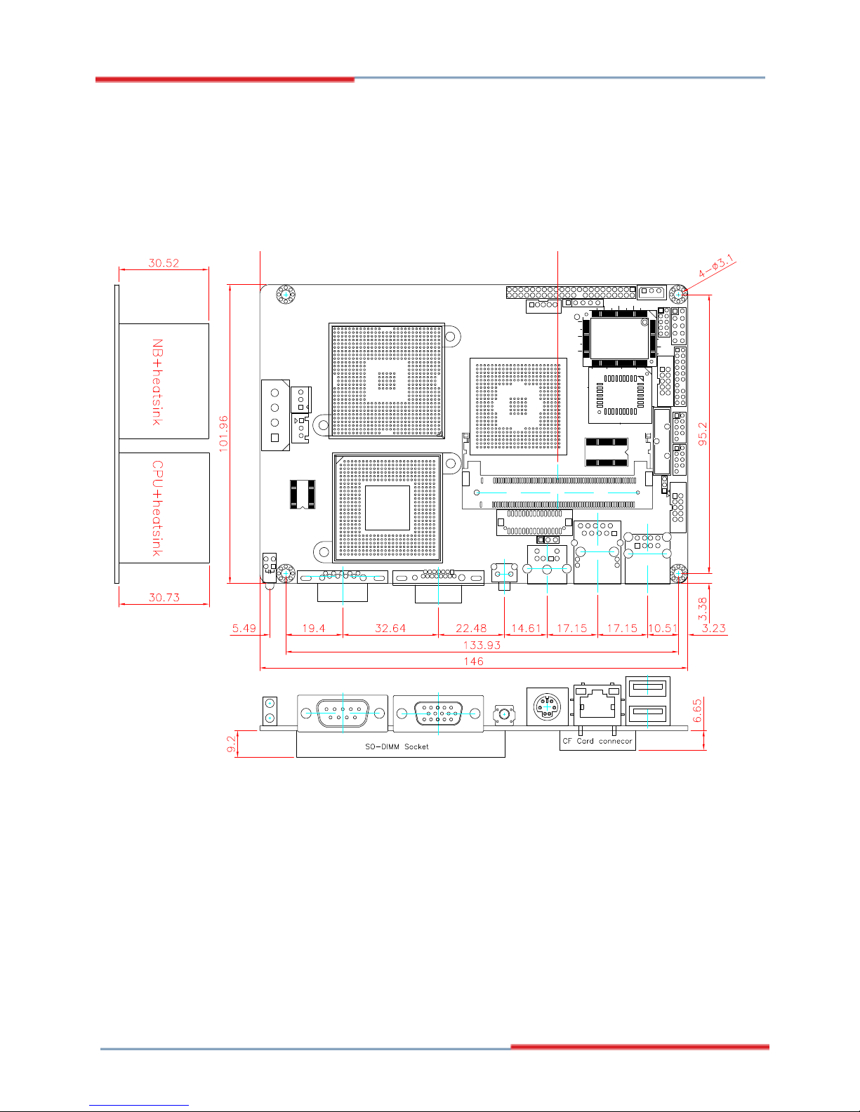
1.11 Board dimensions .............................................................. 8
Chapter 2 Installation ............................................................ 9
2.1 Board layout ........................................................................ 10
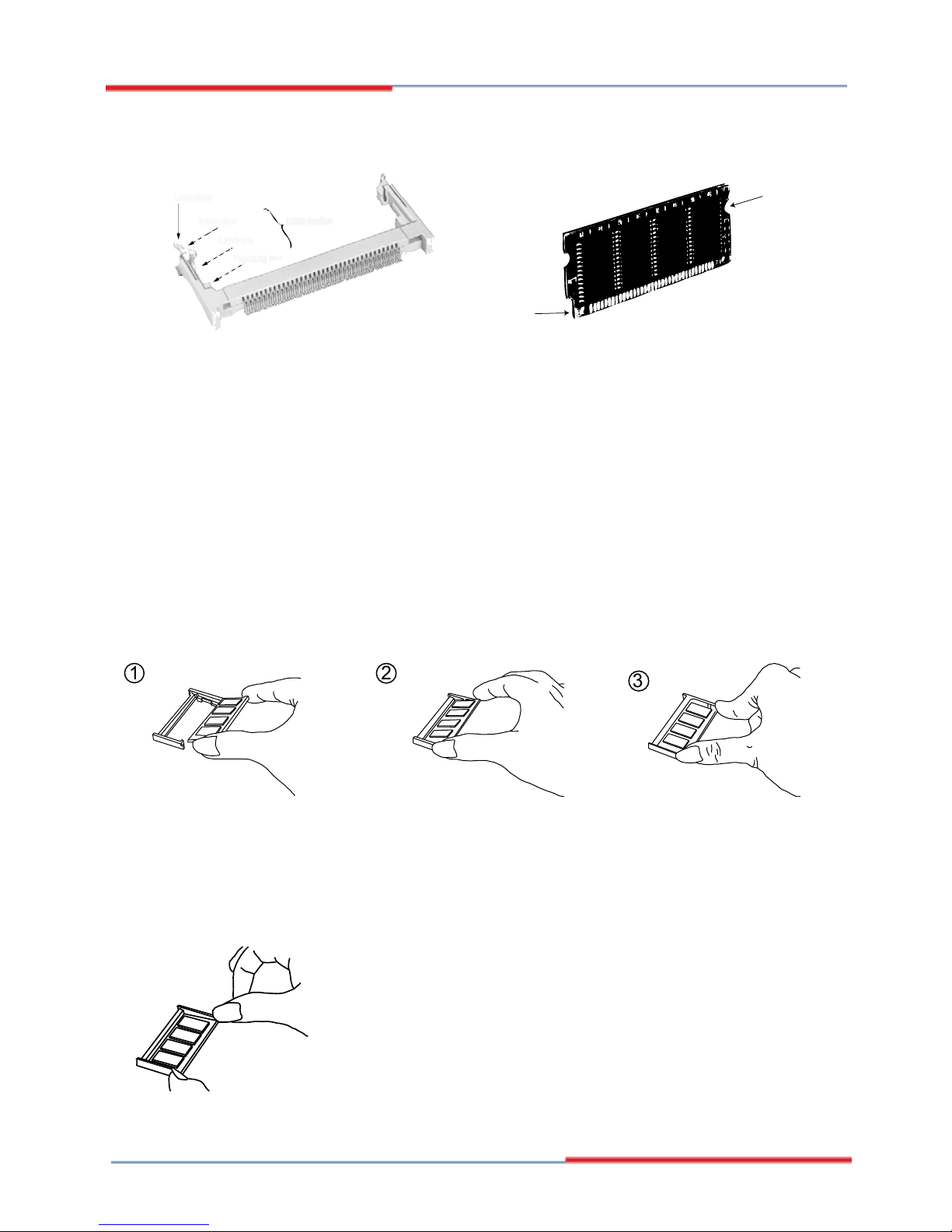
2.2 Jumpers andConnectors ...................................................... 11
Chapter 3 BIOS ...................................................................... 25
3.1 BIOS Introduction ................................................................ 26
3.2 BIOS Setup ......................................................................... 26
3.3 Standard CMOS Features ..................................................... 27
3.4 Advanced BIOS Features ..................................................... 29
3.5 Advanced Chipset Features .................................................. 33
3.6 Integrated Peripherals ..........................................................36
3.8 PNP/PCI Configurations ....................................................... 45
3.9 PC Health Status ................................................................. 46
3.10 Frequency/Voltage Control ................................................. 47
3.12 Set Password .....................................................................48
3.13 Save & Exit Setup ...............................................................49
3.14 Exit Without Saving ............................................................ 49
3.15 BIOS memory map ............................................................. 50
3.16 Award BIOS Post Codes ......................................................50
Chapter 4 Appendix ............................................................... 56
4.1 I/O Map ............................................................................... 57
4.2 IRQ Map ..............................................................................58
4.3 Example of Watch Dog codes ................................................ 58
3.7 Power Management Setup ................................................... 42
3.11 Load Optimized Defaults ..................................................... 47