Gopel Electronic PXI 3080 User manual

Technical Specification
PXI
/
PCI 3080
CAN/ LIN/ K-LINE/ J1850 Interfaces
User Manual
Version 1.5
GOEPEL electronic GmbH
Goeschwitzer Str. 58/60
D-07745 Jena
Phone: +49-3641-6896-597
Fax: +49-3641-6896-944
E-Mail: [email protected]
http://www.goepel.com
Get the total Coverage!

Issue: April 2012
© 2012 GOEPEL electronic GmbH. All rights reserved.
The software described in this manual as well as the manual itself are supplied under license and
may be used or copied only in accordance with the terms of the license.
The customer may make one copy of the software for safety purposes.
The contents of the manual is subject to change without prior notice and is supplied for information
only.
The hardware and software might be modified also without prior notice due to technical
progress.
In case of inaccuracies or errors appearing in this manual, GOEPEL electronic GmbH assumes
no liability or responsibility.
Without the prior written permission of GOEPEL electronic GmbH, no part of this documentation
may be transmitted, reproduced or stored in a retrieval system in any form or by any means
as well as translated into other languages (except as permitted by the license).
GOEPEL electronic GmbH is neither liable for direct damages nor consequential damages from
the company’s product applications.
Printed: 23.04.2012
All product and company names appearing in this manual are trade names or registered trade names of their respective owners.

Table of Contents
PXI 3080/ PCI 3080 – User Manual I
1BOARD INSTALLATION..................................................1-1
1.1 HARDWARE INSTALLATION ...................................................1-1
1.2 DRIVER INSTALLATION........................................................1-2
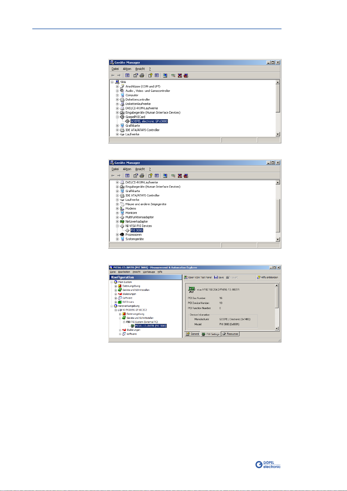
1.2.1
Windows Device Driver ...........................................1-2
1.2.2
VISA Device Driver .................................................1-3
2PXI/ PCI 3080 HARDWARE ...........................................2-1
2.1 DEFINITION .....................................................................2-1
2.2 TECHNICAL DATA ..............................................................2-3
2.2.1
General..................................................................2-3
2.2.2
Dimensions ............................................................2-3
2.2.3
PXI 3080/ PCI 3080 Characteristics..........................2-3
2.3 CONSTRUCTION ................................................................2-4
2.3.1
General..................................................................2-4
2.3.2
Addressing.............................................................2-5
2.3.3
Communication Interfaces.......................................2-6
2.3.4
Assembly ...............................................................2-9
2.3.5
Assignment Frontal Plug Connector........................2-11
2.3.6
LED Display..........................................................2-12
2.4 DELIVERY NOTES.............................................................2-13
3CONTROL SOFTWARE....................................................3-1
3.1 PROGRAMMING VIA G-API.FEHLER!TEXTMARKE NICHT DEFINIERT.
3.2 PROGRAMMING VIA DLL FUNCTIONS.......................................3-3
3.2.1
Windows Device Driver ...........................................3-4
3.2.1.1 Driver Info..........................................................3-5
3.2.1.2 DLL Version ........................................................3-6
3.2.1.3 XILINX Download................................................3-7
3.2.1.4 XILINX Write Data...............................................3-8
3.2.1.5 DPRAM Write Instruction .....................................3-9
3.2.1.6 DPRAM Read Response......................................3-10
3.2.1.7 Reset Port ........................................................3-11
3.2.2
VISA Device Driver ...............................................3-12
3.2.2.1 Init...................................................................3-13
3.2.2.2 Done................................................................3-13
3.2.2.3 Driver Info........................................................3-14
3.2.2.4 XILINX Download..............................................3-15
3.2.2.5 XILINX Write Data.............................................3-16
3.2.2.6 Write Data........................................................3-17
3.2.2.7 Read Data ........................................................3-18
3.2.2.8 Reset Port ........................................................3-19
3.3 PROGRAMMING WITH LABVIEW ..........................................3-20
3.3.1
LabVIEW via the G-API .........................................3-20
3.3.2
LLB using the Windows Device Driver.....................3-20
3.3.3
LLB using the VISA Device Driver...........................3-20
3.4 FURTHER GOEPEL SOFTWARE............................................3-20


Board Installation
PXI 3080/ PCI 3080 – User Manual 1-1
1Board Installation
1.1 Hardware Installation
Please make absolutely certain that all of the installation procedures
described below are carried out with your system switched off and
disconnected from the mains supply.
Please refer also to the user manual of your PXI/ PCI system for
additional installation instructions that possibly have to be followed.
Electro Static Discharge (ESD) can harm your system and destroy
electronic components. This can lead to irreparable damage on both
the PXI/ PCI 3080 controller board and the system hosting the board
as well as to unexpected malfunction of your test system.
Therefore do not touch the board surface or any connector pins and
electronic components.
The PCI™, CompactPCI™ or PXI™ system is to be opened according
to its conditions. A free slot is to be selected in your system.
Now, the slot cover is to be taken away from the slot selected.
To do this, unscrew the fixation screws if necessary and remove the
cover from the slot.
(If it is necessary to exchange transceiver modules, pay attention to
the general rules to avoid electrostatic charging, see the warning
above. Transceiver modules must never be removed or mounted with
the power switched on!
Additionally, the right alignment is absolutely required.)
Insert the board carefully into the prepared slot. For PXI boards, use
the lever at the front plate in order to push in the board finally.
When the board has been inserted properly, it is to be fixed by means
of the screws at the front plate.
Now, the board has been installed correctly.
Afterwards, carry out the operations required at the system to make it
ready for operation anew.

Board Installation
1-2 PXI 3080/ PCI 3080 – User Manual
1.2 Driver Installation
PXI/ PCI 3080 controller boards can be operated under Windows®
2000/ XP as well as under Windows®7/ 64 bit.
Due to the plug and play capability of Windows®, for every newly
recognized hardware component a driver installation is started
automatically via the hardware assistant.
The hardware assistant can carry out the installation of the device
driver by using the
inf
file contained in the
GPxi3080
folder of the
supplied CD.
If necessary, you can find the required
inf
files as follows:
♦
GPxi3080.inf
for Windows®2000/ XP in the
Win2000 (Version xx)
folder
♦
GPxi3080_x64.inf
for Windows®7/ 64 Bit in the
Win7_x64 (Version xx)
folder
It is not absolutely essential to restart the system.
The following step is only required in case you do not use the G-API
(see also Control Software).
If you want to create your own software for the boards, you possibly
need additional files for user specific programming (
*.LLB
,
*.H
).
These files are not automatically copied to the computer and have to
be transferred individually from the supplied CD to your development
directory.
1.2.1
Windows
Device Driver

Board Installation
PXI 3080/ PCI 3080 – User Manual 1-3
First step
Copy the
VISA (Version xx)
directory from the
GPxi3080
folder of
the delivered CD to your hard disk
(recommendation: Complete directory to
C:
\).
Second step
VISA for Windows2000, WindowsXP :
Due to the plug and play capability, for every newly recognized
hardware component a driver installation is started automatically via
the hardware assistant. Follow the instructions. Enter as target
directory the one which contains the
PXI3080_NT5.inf
file
(according to recommendation:
C:
\
VISA (Version xx)
\
Installation
).
VISA for LabViewRT :
For operating PXI/ PCI 3080 boards under the RT operating system,
use the
P3080_RT.inf
file from the
C:
\
VISA (Version xx)
\
Installation
directory.
Copy this file to the \
ni-rt
\
system
folder of the embedded controller.
Use the NI Measurement & Automation Explorer for that.
The connected RT controller can be found under Remote Systems.
Open a pop-up menu by pressing the right mouse button.
In this menu, select the File Transfer entry and follow the instructions.
If you intend to create a
startup.rtexe
later, copy also the
cvi_lvrt.dll
file to the \
ni-rt
\
system
folder.
Third step:
Reboot your computer to complete installation.
1.2.2 VISA
Device Driver

Board Installation
1-4 PXI 3080/ PCI 3080 – User Manual
After hardware and driver installation, you can check whether the
boards are properly imbedded by the system:
Figure 1-1:
Windows
Figure 1-2:
VISA for Windows XP
Figure 1-3:
ViISA for LabVIEW RT

Hardware
PXI 3080/ PCI 3080 – User Manual 2-1
2PXI/ PCI 3080 Hardware
2.1 Definition
The PXI 3080/ PCI 3080 multi-interface-boards are communication
boards of GOEPEL electronic GmbH.
These boards can be used in general control technology, especially for
applications in automotive technology.
A PXI 3080/ PCI 3080 board in the maximum construction stage offers
the following resources:
♦2 x CAN
♦2 x LIN or K-Line
♦1 x J1850 VPW
♦1 x J1850 PWM
(in this case only ONE LIN or K-Line interface is possible)
♦4 x Digital Input
♦4 x Digital Output
♦2 x Analog Input
♦1 x Wake line
The resources are galvanically separated from the PXI/ PCI interface.

Hardware
2-2 PXI 3080/ PCI 3080 – User Manual
Figure 2-1:
PXI 3080
Abbildung 2-2:
PCI 3080

Hardware
PXI 3080/ PCI 3080 – User Manual 2-3
2.2 Technical Data
The PXI 3080 communication board is a plug-in board developed for
the PXI™ bus (PCI eXtensions for Instrumentation). Basis of this bus
is the CompactPCI™ bus.
The board can be plugged into any desired slot of a CompactPCI™ or
PXI™ system (except for slot 1). It can be definitely identified also in
the case that several boards of this type are used in the same rack.
The PCI 3080 communication board is a PC plug-in board for the PCI
Local Bus Rev. 2.2.
It can be operated at any PCI slot (32 bits, 33 MHz, 3.3 V)
Both boards do not have jumpers for hardware detection and are
automatically integrated into the respective system.
The dimensions of both boards correspond to standard dimensions of
the accompanying bus system:
♦PXI 3080 Multi Interface Board: 160 mm x 100 mm (L x W)
♦PCI 3080 Multi Interface Board: 168 mm x 106 mm (L x W)
Symbol Parameter Min. Typ. Max. Unit Remarks
VBAT Battery voltage 12 27/ 50 V Acc. to transceiver’s type
Transmission rate 1 MBaud CAN
Transmission rate 22 kBaud LIN
Rbus Terminating resistor 1 120 Ohms CAN jumper plugged in
Rbus Terminating resistors 2 10 kOhms CAN jumper plugged in
RPullup Pull-up resistor 680 Ohms K-Line jumper plugged in
Vin Input voltage 3.3 50 V Digital input
Vout Output voltage VBAT V Digital output, OC
Vin Input voltage 26 V Analog input
Viso Galvanic separation 1000 V PXI/ PCI Input/ Output
The Analog input channels are designed with the LTC 1400
(analog-to-digital transducer) of Linear Technology.
This component has a Resolution of 12 Bits and an Input voltage
range of 0..4.095V.
Caused by the input voltage divider (122K/22K) the following results
for the measured voltage:
Vmeas = AD transducer value * 1mV * (122K/22K).
2.2.1 General
2.2.2 Dimensions
2.2.3
PXI 3080/
PCI 3080
Characteristics

Hardware
2-4 PXI 3080/ PCI 3080 – User Manual
2.3 Construction
An ASIC is used as the interface to the PCI or cPCI bus on the PXI/
PCI 3080 boards. It includes all the function blocks required for the
communication with the computer bus.
The PCI 3080 communication board does not have a PXI interface.
To exchange trigger signals with other GOEPEL electronic PCI boards
despite of that, an additional plug connector is on this board with two
lines configurable as input or output (J902 in Figure 2-7).
Figure 2-3: Block diagram of a PXI/ PCI 3080 Communication Board
PCI bus
interface
TC1775
serial0
CAN0
J1850 serial1
CAN1
Transceiver
plug-in place
Transceiver
plug-in place
Transceiver
plug-in place
Transceiver
plug-in place
Transceiver
plug-in place
Dig_In Dig_Out
AD
transducer
Optical
coupling
device
UBat/
Ground
K-Line/LIN
K-Line/LIN
CAN
CAN
J1850
Digital
Out (UBat)
Digital
In (Ubat)
2xAnalog
In (0-20V)
DSub
RAM/
Flash... DC/DC
transducer
Wake
line
Flash interface
2.3.1 General

Hardware
PXI 3080/ PCI 3080 – User Manual 2-5
PXI 3080: PXI racks do have an own geographical slot addressing of
the backplane. Numbering starts with 1and can be seen at the
cover’s front side. Mount always an embedded controller or an MXI
card at slot 1.
The PXI 3080 board can read out this geographical slot address. For
that the belonging FPGA file has to be loaded to the XILINX (see the
XilinxDownload functions for different drivers in the Control Software
section).
PCI 3080: PCI racks do not have an own geographical slot
addressing. There is a separate DIP switch (S900 in Figure 2-7) for
clear identification of the board in a system with several PCI 3080
boards. You can select up to 16 addressing variants by this. The
corresponding binary value (0to 15) set with the S900 switch can be
read out by the delivered software.
2.3.2 Addressing

Hardware
2-6 PXI 3080/ PCI 3080 – User Manual
2 x CAN Interface Version 2.0b:
The type of the mounted transceiver is decisive for proper operation
of a CAN interface in a network. Often CAN networks do only operate
properly in the case that all members use a compatible type of
transceiver.
To offer maximal flexibility to the users of the PXI/ PCI 3080 boards,
the transceivers are designed as plug-in modules. There are several
types (high speed, low speed, single-wire etc.) that can be easily
exchanged.
Not only the type of the mounted transceiver, but also the terminating
resistor of the bus is very important for proper operation of a CAN
network.
For the use of highspeed CAN transceivers, usually one 120 Ohm
resistor is active on each CAN interface.These resistors can be
deactivated by removing the J1401 or J1501 jumpers.
In the case of lowspeed CAN transceivers, usually two resistors with a
resistance value of 10 kOhm for RTH and RTL are active for each
CAN interface (by inserting the J1402/ J1403 or J1502/ J1503
jumpers). Then the J1401 or J1501 jumpers must NOT be
plugged-in.
2.3.3 Commu-
nication Interfaces
Figure 2-4:
CAN Interface

Hardware
PXI 3080/ PCI 3080 – User Manual 2-7
2 x K-Line Interface (ISO 9141) or
2 x LIN Interface Version 2.0:
K-Line:
The transceivers are designed as plug-in modules. Generally, the
L9637 of ST is used for this type of transceicer.
Via the VBat contacts the power supply of the transceiver modules is
connected. To bridge the reverse-connect protection diode for VBatfor
LIN, the J1602 or J1703 jumpers must be plugged-in.
In the case the pull-up resistor to VBat is to be activated, the J1601
or J1701 jumpers must be plugged-in.
LIN:
The transceivers are designed as plug-in modules. Generally, the
TJA1020 of Philips is used for this type of transceicer.
For the standard design of the transceiver modules, it is possible to
change over between Master and Slave configuration per software
using the Rel1 relay for LIN1 and Rel2 for LIN2. The pull-up resistors
for LIN are located on the transceiver module. Therefore the J1601
or J1701 jumpers must NOT be plugged-in.
Via the VBat contacts the power supply of the transceiver modules is
connected. According to the LIN specification, this power supply is to
be carried out via a reverse-connect protection diode. Therefore the
J1602 or J1703 must NOT be plugged-in.
Figure 2-5:
LIN/ K-Line Interface

Hardware
2-8 PXI 3080/ PCI 3080 – User Manual
J1850 Interfaces:
The transceivers are designed as plug-in modules.
Generally, the AU5780 of Philips is used for J1850 VPW
transceivers.
The output circuitry of a J1850 PWM transceiver is realized by discrete
components.
The transceiver for a J1850 VPW interface has to be inserted at the
position for J1850 transceivers.
On the other hand, the transceiver for a J1850 PWM interface must be
inserted at the position for a K-Line/ LIN 2 transceiver
(see Figure 2-6 and Figure 2-7).
J1701 must NOT be mounted in the case of a J1850 PWM
interface!

Hardware
PXI 3080/ PCI 3080 – User Manual 2-9
Figure 2-6 and Figure 2-7 show schematically the component side of
the boards. You can see the positions of the transceiver modules, plug
connectors, DIP switches and jumpers.
Figure 2-6: Component side of a PXI 3080 communication board (schematically)
Figure 2-7: Component side of a PCI 3080 communication board (schematically)
The transceiver for a J1850 VPW interface has to be inserted at the
position for J1850 transceivers.
On the other hand, the transceiver for a J1850 PWM interface must
be inserted at the position for a K-Line/ LIN 2 transceiver.
XS 1
Transceiver-
Module
K-Line/LIN2
1
1
S301
Transceiver-
Module
K-Line/LIN1
1
Transceiver-
Module
J1850
Transceiver-
Module
CAN2
Transceiver-
Module
CAN1
1
1
1
J1701 J1601 J1602
J1403 J1502
J1703
J1402 J1501J1503
J1401
ON
XS 1
Transceiver-
Module
K-Line/LIN2
1
1
S301
Transceiver-
Module
K-Line/LIN1
1
Transceiver-
Module
J1850
Transceiver-
Module
CAN2
Transceiver-
Module
CAN1
1
1
1
J1701 J1601 J1602
J1403 J1502
J1703
J1402 J1501J1503
J1401
ON
Transceiver-
Module
K-Line/LIN2
1
XS 1
J902
1
ON
S900
1
ON
S301
Transceiver-
Module
K-Line/LIN1
1
Transceiver-
Module
J1850
Transceiver-
Module
CAN2
Transceiver-
Module
CAN1
1
1
1
J1703 J1701 J1601 J1602
J1401
J1402
J1403 J1501
J1502
J1503
2.3.4 Assembly

Hardware
2-10 PXI 3080/ PCI 3080 – User Manual
The configuration elements of Figure 2-6 and Figure 2-7 are
explained in the following table:
XS1401 Transceiver module for CAN1
J1401 Jumper to activate the 120Ω terminating resistor for CAN1
J1402 Jumper to activate the RTH 10kΩ terminating resistor for CAN1
J1403 Jumper to activate the RTL 10kΩ terminating resistor for CAN1
XS1501 Transceiver module for CAN2
J1501 Jumper to activate the 120Ω terminating resistor for CAN2
J1502 Jumper to activate the RTH 10kΩ terminating resistor for CAN2
J1503 Jumper to activate the RTL 10kΩ terminating resistor for CAN2
XS1601 Transceiver module for LIN1/ K-Line1
J1601 Jumper to activate the 680Ω pull-up resistor to VBAT for K-Line1
J1602 Jumper to bridge the reverse-connect protection diode for VBat for LIN1
XS1701 Transceiver module for LIN2/ K-Line2/ J1850 PWM
J1701 Jumper to activate the 680Ω pull-up resistor to VBAT for K-Line2
J1703 Jumper to bridge the reverse-connect protection diode for VBat for LIN2
XS1801 Transceiver module for J1850 VPW
S301 DIP switches of the PXI/ PXI 3080 boards to configurate the micro controller.
Do NOT change the settings!
S900 This DIP switch on a PCI 3080 board is for clear identification of the board
(analogously to “geographical addressing” of the PXI specification) in a system with
several PCI 3080 boards.
You can select up to 16 addressing variants this way (0..15).
The corresponding binary value set with the S900 switch can be read out by the
delivered software.
J902 Plug connector to exchange trigger signals with other GOEPEL electronic PCI boards

Hardware
PXI 3080/ PCI 3080 – User Manual 2-11
Type: DSub 25 poles socket
The interfaces are provided via this plug connector at the frontal edge
of the PXI/ PCI 3080 communication boards.
The pinout of both boards is identical according to the following table:
No. XS1 pin Signals name Remarks
1 1 CAN1_High
2 14 CAN1_Low
3 2 CAN2_High
4 15 CAN2_Low
5 3 VBAT Reference potential plus transceiver
6 16 GND Ground potential transceiver
7 4 K-Line1/ LIN1 depending on transceiver
8 17 L-Line1/ WAKE1 depending on transceiver
9 5 K-Line2/ LIN2/ J1850 PWM+ depending on transceiver
10 18 L-Line2/ WAKE2/ J1850 PWM- depending on transceiver
11 6 J1850 VPW
12 19 - Please do not assign
13 7 VBAT Reference potential plus transceiver
14 20 GND Ground potential transceiver
15 8 Analog Input1
16 21 Analog Input2
17 9 Digital Input1
18 22 Digital Output1
19 10 Digital Input2
20 23 Digital Output2
21 11 Digital Input 3
22 24 Digital Output3
23 12 Digital Input 4
24 25 Digital Output4
25 13 Wake line
For K-Line the connections for the L-Line are wired to PIN 17/ 18 if
necessary (depending on the output circuitry).
For LIN the connections for the Wake-Line are wired to PIN 17/ 18
if necessary (depending on the selection of the transceiver).
The pins 3 and 7 as well as 16 and 20 are bridged on the board!
2.3.5 Frontal
Plug Connector
Pinout

Hardware
2-12 PXI 3080/ PCI 3080 – User Manual
The LEDs indicate the following states:
♦Red LED D100: /HDRST hardware reset indication output of the
micro controller
♦Green LED D700: Voltage 5V status
♦Green LED D701: Voltage 3.3V status
♦Green LED D702: Voltage 2.5V status
♦Yellow LED D801: Micro controller CAN 1 status
♦Yellow LED D802: Micro controller CAN 2 status
♦Yellow LED D803: Micro controller K-Line/ LIN 1 status
♦Yellow LED D804: Micro controller K-Line/ LIN 2 status
The LEDs are arranged as follows at the front panel:
D702 D701 D700 D100
D801 D802 D803 D804
2.3.6 LED Display
This manual suits for next models
1
Table of contents
Other Gopel Electronic Recording Equipment manuals