PHASE I
BREADBOARD
tn this phase,you will have an opportunity to construct an experimental
breadboard similar to that used by engineers and technicians in industry.
A breadboard is a layout of electronic parts, wired in such a way that
the parts may be easily added or removed during experimental work.
DISCUSSION
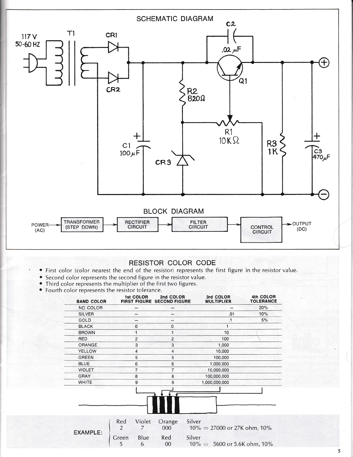
Your Model 803 solid-state Power Supply consists of four
stages of circuitry: power transformer circuit, rectifier circuit,
filter circuit, and voltage control circuit. ln this phase you
will study the operation of your power supply by bread-
boarding one stage at a time.
TRANSFORMER EXPERIENCE
DISCUSSION
A transformer is an alternating current (AC) device that
transfers electrical energy from one circuit to another. lt is
usually used to STEP UP or to STEP DOWN an AC voltage.
ln its basic form, the transformer consists of two coils of
wire wound around an iron core. One coil is connected to
the AC source voltage and is called the PRIMARY winding;
the other coil is called the SECONDARY winding and pro-
vides the proper supply voltage.
The transformer used in this power supply is a step-down
transformer with a center-tap on the secondary winding,
as illustrated by the schematic symbol shown in Fig. A.
The application of two important laws in electricity make
transformers possible. They are: (1) An electric current flow-
MAGNETIC FIELD
ing through a coil produces a magnetic field that varies w'ith
the current; and (2) A magnetic field cutting across the wires
in a coil induces a voltage in the coil. Transformer action is
illustrated in Fig. B. It shows that the changing magnetic
field, created by the varying current in the primary winding,
induces a voltage in the secondary winding as the magnetic
field cuts across the turns of wire in this coil.
The relationship between the input voltage (primary) and
the output voltage (secondary) is determined by the number
of turns of wire in the primary and the number of turns of
wire in the secondary. This relationship is called the TURNS-
RATIO and is expressed mathematically as,
Eprimary _ N primary
Esecondary " N secondary
where,
E is voltage and N the number of turns.
For example: a transformer has 1,000 turns in the primary
and 500 turns in the secondary. lf a voltage of 1-10 volts AC
is applied to the primary, the secondary voltage will be 55
volts AC.
That is, 110 '1000
tsecondary 500
Esecondary : -ry
1000
Esecondary : 55 V
CONSTRUCTION
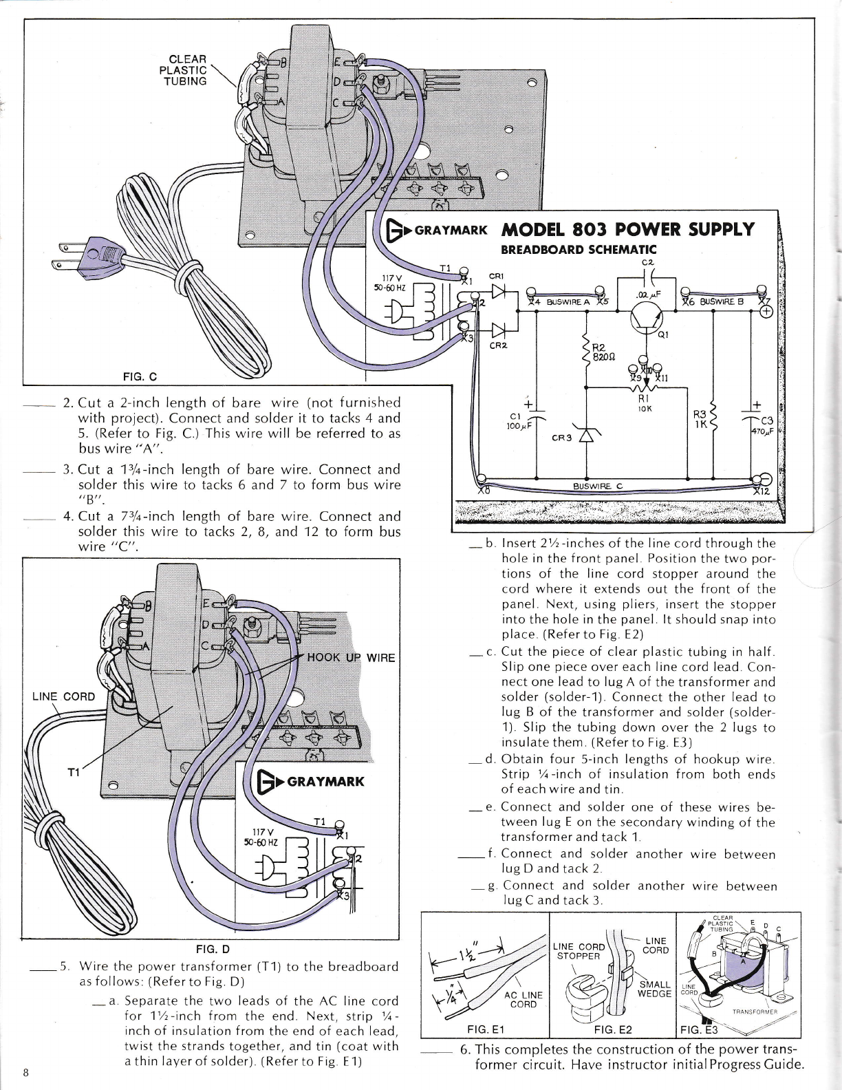
Cut out and fasten the BREADBOARD SCHEMATIC on page
23 to a flat piece of wood. This will serve as a breadboard
base upon which you will construct your experimental cir-
cuits. You will need to obtain the following items not fur-
nished with your project: (1) Twelve copper tacks (or brass
brads); (2) A 12-inch length of bare copper wire; and (3)
Four pieces of hookup wire, each 5-inches in length. 'DO
NOT CUT THE LEADS of any components unless instructed
to do so, because these components will be used for con-
structing other circuits. Caution: Do not disturb the mount-
ing of transistor Q1 . However, if it becomes necessary to
remove it, be sure the insulating washers are replaced
properly.
-- 1. Insert a tack into the breadboard at X marks 1
through 12 on the schematic.
FIG. ,ll,tlll|llll,ll,lllllll,l,]ll|l|lill,t,:l|llIl|lllllll|
CENTER-TAP
PRIMARY
WINDING
SECONDARY
WINDING
STEP-DOWN
FIG. A