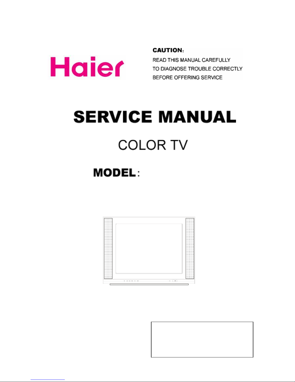
Haier HTR20-A User manual
1
HTR20-A
(TMPA8873PSCNG)
All rightsreserved. Unauthorized copying and distribution is a
violation of law.

2
WARNING
This service information is designed for experienced repair technicians only and is not designed for use
by the general public. It does not contain warnings or cautions to advise non-technical individuals of
potential dangers in attempting to service a product. Products powered b electricity should be serviced
or repaired only by experienced professional technicians. Any attempt to service or repair the product
deal with in this service information by anyone else could result in serious injury or death.
CONTENT
1. SPECIFICATIONS………………………………………………………………………….. 3
2. WAINING…………………………………………………………………………………….. 4
3. FEATURESAND TECHINICAL DESCRIPTION………………………………………... 11
4. Adjustment……………………………………………………………………………………11
5. WIRING CONNECTION DIAGRAM……………………………………………………….21
6. Circuit Explanation…………………………………..…………………..…………….……21
7. Maintenance Service and Trouble shooting………………………………………………24
8 .Circuit Diagram………………………………..……………………………………………..29
3
1. Specification
MODEL
21T07
MODEL
21T07
NO.
ITEM
FUNCTION
USA
NO.
ITEM
FUNCTION
USA
1 Main IC TMPA8873PSCNG 24 Digital curtain ×
2 CRT flat 25 Slow fading on & off ×
3 Color system NTSC+ATSC 26 Semitransparent menu √
4 Audio system M 27
N
on-flshing channel changing √
5
N
O.of channels 181 28 ZOOM √
6 OSD language ENGLISH/F/S 29 16:9 mode √
7
PICTURE
Multi-picture modes 4 30 Games ×
8 AV stereo √ 31 Calendar ×
9 Super woofer × 32 Child-lock ×
10 Surrounding sound × 33 V-CHIP √
11 Treble/bass boost × 34
N
o-picture listening ×
12 Left/right balancer √ 35 Background light ×
13
N
ICAM × 36 Sleep timer √
14 Multi-audio modes × 37 Q.view √
15 Tone adjuster × 38
SOFTWARE
CCD √
16 MTS/SAP √ 39
N
O. of buil
t
-in speakers 2
17
AUDIO
Auto-volume leveling × 40 Audio output power(W) 2×2
18 AV input back 1,front1 41 Total power input(W)85
19 AV output back 1 42 Voltage range(V)AC120
20 DVD terminal back 1 43 Power frequency(Hz)60
21 S-video jack back 1 44 Time of sleep timer(MINS) 240
22 Headphone socket √45
N
et weight(KG) 24
23
JACK
SCART socket × 46 Gross weight(KG) 26
47
N
et dimension(MM) 576×395×458
48
PARAMETER
Packaged dimension(MM) 650×565×525

4
2.Warning
Safety Precautions
IMPORTANT SAFETY NOTICE
Many electrical identify these parts and mechanical parts in this chassis have special
safety-related characteristics! In the Schematic Diagram and Replacement Parts List.
It is essential that these special safety parts should be replaced with the same
components as recommended in this manual to prevent X-RADIATION, Shock, Fire, or
other Hazards.
Do not modify the original design without permission of the manufacturer.
General Guidance
An Isolation Transformer should always be used during the servicing of a receiver whose
chassis is not isolated from the AC power line. Use a transformer of adequate power rating
as this protects the technician from accidents that might result in personal injury caused by
electrical shocks.
It will also protect the receiver and it’s components from being damaged by accidental
shorts of the circuitry that might be inadvertently introduced during the service operation.
If any fuse (or Fusible Resistor) in this TV receiver is blown, replace it with a specified one.
When replacing a high wattage resistor (Oxide Metal Film Resistor, over 1W), keep the
resistor 10mm away from PCB.
Keep wires away from high voltage or high temperature parts.
Due to the high vacuum and large surface area of the picture tube, extreme care should be
taken in handling the Picture Tube. Do not lift the Picture Tube by its Neck.
X-RAY Radiation
Warning:
The source of X-RAY RADIATION in this TV receiver is the High Voltage Section and the
Picture Tube.
For continued X-RAY RADIATION protection, the replacement tube must be of the same
type as specified in the Replacement Parts List.
Before returning the receiver to the customer,
Always perform an AC leakage current check on the exposed metallic parts of the cabinet,
such as antennas, terminals, etc., to make sure that the set is safe to operate without any
danger of electrical shock.

5
Warning and Cautions
1. When you clean the TV set, please pull
out the power plug from AC outlet. Don't
clean the cabinet and the screen with
benzene,petrolandotherchemicals.
4. To prevent the TV set from firing and
electricshock,don't
maketheTVsetrain
ormoisture.
2.
In order to prolong the using life of the
TV set, please place it on a ventilated
place.
5.Don'topenthebackcover,otherwiseitis
possibletodamagethecomponentsinthe
TVsetandharmyou.
3.
Don't place the
TV set in the
sunshine or near
heatsource.
6. When the TV set isn't going to be used
for long time or it is in thunder and
lightening,pleasepulloutthe plug fromAC
outlet and theantennaplugfrom thecover
oftheTVset.
Explanation on the display tube
Generally, it is not needed to clean the tube surface. However, if necessary,its surface can be
cleaned with adry cotton cloth after cutting off the power.Don't use any cleanser. If using hard
cloth, the tube surface will be damaged.
CAUTION: Before servicing receivers covered by this service manual and its supplements
and addenda, read and follow the SAFETY PRECAUTIONS.
NOTE: If unforeseen circumstances create conflict between the following servicing
precautions and any of the safety precautions, always follow the safety precautions.
Remember: Safety First.

6
General Servicing Precautions
1. Always unplug the receiver AC power cord from the AC power source before:
a. Removing or reinstalling any component, circuit board module or any other
assembly of the receiver.
b. Disconnecting or reconnecting any receiver electrical plug or other electrical
connection.
c. Connecting a test substitute in parallel with an electrolytic capacitor in the receiver.
CAUTION: A wrong substitution part or incorrect installation polarity of electrolytic
capacitors may result in an explosion hazard.
d. Discharging the picture tube anode.
2. Test high voltage only by measuring it with an appropriate high voltage meter or other
voltage-measuring device (DVM, FETVOM, etc.) equipped with a suitable high voltage
probe. Do not test high voltage by “drawing an arc”.
3. Discharge the picture tube anode only by (a) first connecting one end of an insulated
clip lead to the degaussing or kine aquadag grounding system shield at the point where
the picture tube socket ground lead is connected, and then (b) touch the other end of
the insulated clip lead to the picture tube anode button, using an insulating handle to
avoid personal contact with high voltage.
4. Do not spray chemicals on or near this receiver or any of its assemblies.
5. Unless specified otherwise in this service manual, clean electrical contacts only by
applying the following mixture to the contacts with a pipe cleaner, cotton-tipped stick or
comparable nonabrasive applicator; 10% (by volume) Acetone and 90% (by volume)
isopropyl alcohol (90%-99% strength)
CAUTION: This is a flammable mixture.
Unless specified otherwise in this service manual, lubrication of contacts is not
required.
6. Do not defeat any plug / socket B+ voltage interlocks with which receivers covered by
this service manual might be equipped.
7. Do not apply AC power to this instrument and/or any of its electrical assemblies unless
all solid-state device heat sinks are correctly installed.
8. Always connect the test receiver ground lead to the receiver chassis ground before
connecting the test receiver positive lead.
Always remove the test receiver ground lead last.
9. Use with this receiver only the test fixtures specified in this service manual.
CAUTION: Do not connect the test fixture ground strap to any heat sink in this receiver.
Electrostatic ally Sensitive (ES) Devices
Some semiconductor (solid state) devices can be damaged easily by static electricity.
Such components are usually called Electrostatic ally Sensitive (ES) Devices. Examples of

7
typical ES devices are integrated circuits and some field effect transistors and
semiconductor “chip” components. The following techniques should be used to help
reduce the incidence of component damage caused by static electricity.
1. Immediately before handling any semiconductor component or semiconductor-
equipped assembly, drain off any electrostatic charge on your body by touching a
known earth ground. Alternatively, obtain and wear a commercially available
discharging wrist strap device, which should be removed to prevent potential shock
prior to applying power to the unit under test.
2. After removing an electrical assembly equipped with ES devices, place the assembly
on a conductive surface such as aluminum foil, to prevent electrostatic charge buildup
or exposure of the assembly.
3. Use only a grounded-tip soldering iron to solder or unsolder ES devices.
4. Use only an anti-static type folder removal device. Some solder removal devices not
classified as “anti-static” can generate electrical charges sufficient to damage ES
devices.
5. Do not use freon-propelled chemicals. These can generate electrical charges
sufficient to damage ES devices.
6. Do not remove a replacement ES device from its protective package until immediately
before you are ready to install it. (Most replacement ES devices are packaged with
leads electrically shorted together by conductive foam, aluminum foil or comparable
conductive material).
7. Immediately before removing the protective material from the leads of a replacement
ES device, touch the protective material to the chassis or circuit assembly into which
the device will be installed.
CAUTION: Be sure no power is applied to the chassis or circuit, and observe all other
safety precautions.
8. Minimize bodily motions when handling unpackaged replacement ES devices.
(Otherwise even some normally harmless motions such as mutual brushing of your
clothes’ fabric or lifting of your foot from a carpeted floor might generate static electricity
sufficient to damage an ES device.)
General Soldering Guidelines
Use a grounded-tip, low-wattage soldering iron and appropriate tip size and shape that
will maintain tip temperature within the range of 500oF to 600oF.
Use an appropriate gauge of RMA resin-core solder composed of 60 parts tin/40 parts
lead.
Keep the soldering iron tip clean and well tinned.
Thoroughly clean the surfaces to be soldered. Use a mall wire bristle (0.5 inch, or 1.25cm)
brush with a metal handle. Do not use freon-propelled spay-on cleaners.
Use the following unsoldering technique
a. Allow the soldering iron tip to reach normal temperature. (500o F to 600o F)

8
b. Heating the component lead until the solder melts.
c. Quickly draw the melted solder with an anti-static, suction-type solder removal
device with solder braid.
CAUTION: Work quickly to avoid overheating the circuit board printed foil.
Use the following unsoldering technique
a. Allow the soldering iron tip to reach normal temperature. (500o F to 600o F)
b. First, hold the soldering iron tip and solder the strand against the component lead
until the solder melts.
c. Quickly move the soldering iron tip to the junction of the component lead and the
printed circuit foil, and hold it there only until the solder flows onto and around both
the component lead and the foil.
CAUTION: Work quickly to avoid overheating the circuit board printed foil.
d. Closely inspect the solder area and remove any excess or splashed solder with a
small wire-bristle brush.
Remove /Replacement
Some chassis circuit boards have slotted holes (oblong) through which the IC leads are
inserted and then bent flat against the circuit foil. When holes are of slotted type, the
following technique should be used to remove and replace the IC. When working with
boards using the familiar round hole, use the standard technique as outlined.
Removal
Desolder and straighten each IC lead in one operation by gently prying up on the lead with
the soldering iron tip as the solder melts.
Draw away the melted solder with an anti-static suction-type solder removal device (or with
solder braid) before removing the IC.
Replacement
Carefully insert the replacement IC in the circuit board.
Carefully bend each IC lead against the circuit foil pad and solder it.
Clean the soldered areas with a small wire-bristle brush. (It is not necessary to reapply
acrylic coating to the areas).
“Small-Signal” Discrete Transistor
Removal/Replacement
Remove the defective transistor by clipping its leads as close as possible to the
component body.
Bend into a “U” shape the end of each of three leads remaining on the circuit board.
Bend into a “U” shape the replacement transistor leads.
Connect the replacement transistor leads to the corresponding leads extending from the

9
circuit board and crimp the “U” with long nose pliers to insure metal to metal contact then
solder each connection.
Power Output, Transistor Device
Removal/Replacement
Heat and remove all solder from around the transistor leads.
Remove the heat sink mounting screw (if so equipped).
Carefully remove the transistor from the heat sink of the circuit board.
Insert new transistor in the circuit board.
Solder each transistor lead, and clip off excess lead.
Replace heat sink.
Diode Removal/Replacement
Remove defective diode by clipping its leads as close as possible to diode body.
Bend the two remaining leads perpendicularly to the circuit board.
Observing diode polarity, wrap each lead of the new diode round the corresponding lead
on the circuit board.
Securely crimp each connection and solder it.
Inspect (on the circuit board copper side) the solder joints of the two “original” leads. If they
are not shiny, reheat them and if necessary, apply additional solder.
Fuse and Conventional Resistor
Removal/Replacement
1. Clip each fuse or resistor lead at top of the circuit board hollow stake.
2. Securely crimp the leads of replacement component around notch at stake top.
3. Solder the connections
CAUTION: Maintain original spacing between the replaced component and adjacent
components and the circuit board to prevent excessive component temperatures.
Circuit Board Foil Repair
Excessive heat applied to the copper foil of any printed circuit board will weaken the
adhesive that bonds foil to the circuit board causing the foil to separate from or “lift-off” the
board. The following guidelines and procedures should be followed whenever this
condition is encountered.
At IC Connections
To repair a defective copper pattern at IC connections use the following procedure to
install a jumper wire on the copper pattern side of the circuit board. (Use this technique
only on IC connections).
1. Carefully remove the damaged copper pattern with a sharp knife. (Remove only as
much copper as absolutely necessary).
10
2. Carefully scratch away the solder resist and acrylic coating (if used) from the end of
the remaining copper pattern.
3. Bend a small “U” in one end of a small gauge jumper wire and carefully crimp it around
the IC pin. Solder the IC connection.
4. Route the jumper wire along the path of the out-away copper pattern and let it overlap
the previously scraped end of the good copper pattern. Solder the overlapped area
and clip off any excess jumper wire.
At other connections
Use the following technique to repair the defective copper pattern at connections other
than IC Pins. This technique involves the installation of a jumper wire on the component
side of the circuit board.
Remove the defective copper pattern with a sharp knife.
Remove at least 1/4 inch of copper, to insure that a hazardous condition will not exist if
the jumper wire opens.
Trace along the copper pattern from both sides of the pattern break and locate the
nearest component that is directly connected to the affected copper pattern.
Connect insulated 20-gauge jumper wire from the lead of the nearest component on one
side of the pattern break to the lead of the nearest component on the other side.
Carefully crimp and solder the connections.
CAUTION: Be sure the insulated jumper wire is dressed so that it does not touch
components or sharp edges.
WARNING
RISKELECTRIC SHOCK
DONOT OPEN
WARNING:To reduce the risk of electric shick don’t remove cover or back.
No user-serviceable parts inside refer service to qualified service personnel.
Safety of operators has been taken into consideration at the design and manufacture phase, but
inappropriate operation may cause electric shock or fire. To prevent the productfrom being damaged,
the following rules should be observed for the installation, use and maintenance of th product. Read the
following safety instruction before starting the operation.
The User Manual uses the following symbols to ensure a safe operation and preventany damage to
operators or properties:

11
3.FEATURES AND TECHINICAL DESCRIPTION
FUNCTIONS :
1.181 channels 2.I2C bus control
3.Auto scan 4.Audio/video input/output interfaces
5.Multiple picture modes selection 6.Blue screen
7NTSC+ATSC 8.CCD
9.SLEEPTIMER 10.Q.VIEW
11.V-CHIP 12.ARC(LETTERBOX/ZOOM/FULL)
4. Adjustment
A..Factory adjustment information
Specific operation: use remote controller
Press “MENU” Æ“8”Æ”8”Æ”9”Æ”3” buttons in sequence to enter into factory
mode.Press “MENU” to enter into next factory menu.
Press [CH+] / [CH-] to select items and press [VOL+] / [VOL-] key, to make data
adjustment of corresponding factory menus.
Press “EXIT” key to exit factory mode.
B.Maintenance menu (Table 8)
You can change the DATA with “*” mark when necessary.
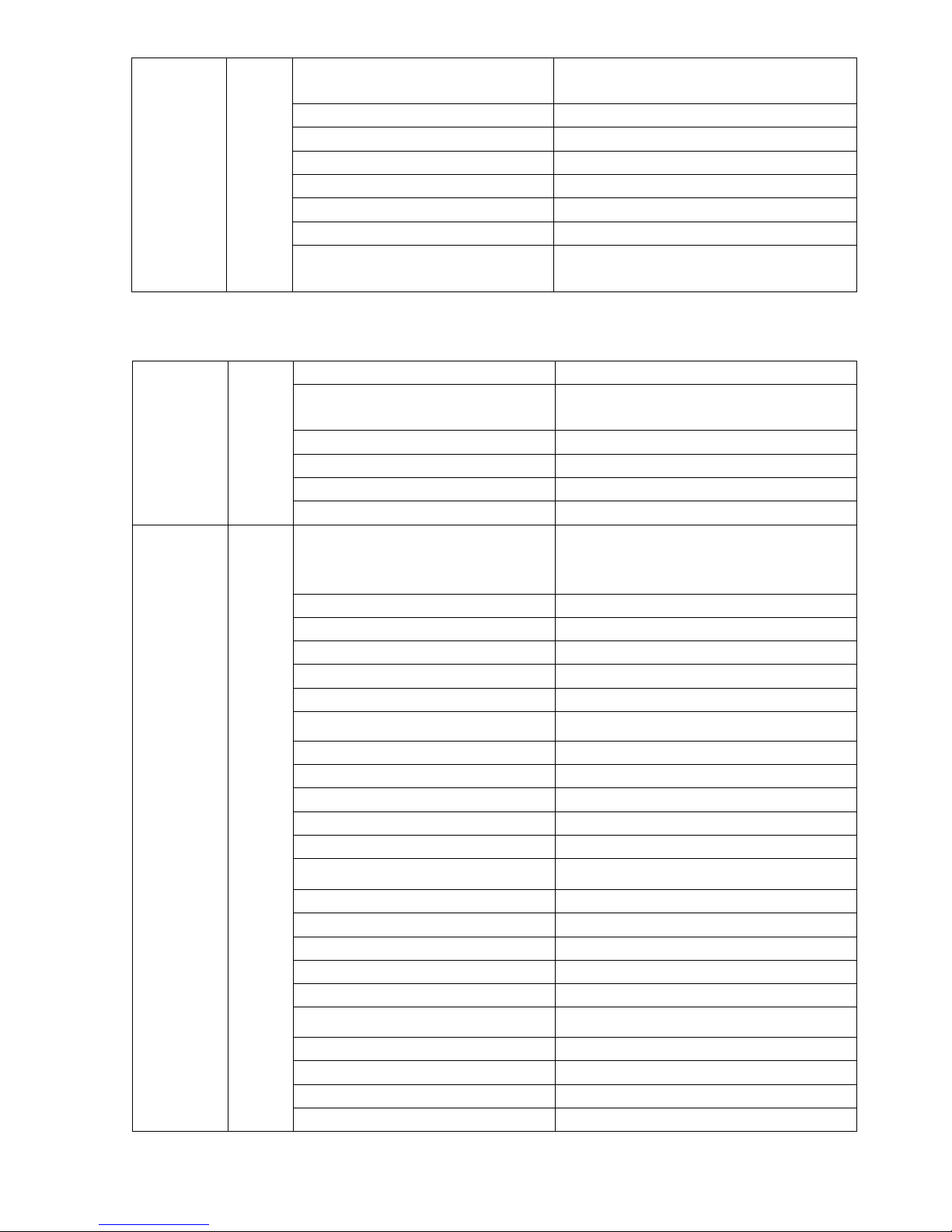
MENU 00
Items
Preset Description predicament
HPOS 0E
60Hz Horizontal shift
VPOS 03 60Hz Vertical shift
00:+20%
VSC 15 S emendation 1F:-20%
00:-12%
10:0%
VLIN 0C Vertical slop 1F:12%
HIT 32 60Hz Vertical amplitude
HBOW 03 H BOW emendation
HPARA 04 H PAPR emendation
00:-20%
20:0%
VCEN 17 Vertical centering 3F:20%
MENU 01
Items
Preset Description predicament

12
HPOS-D 00
DTV Horizontal shift
VPOS-D 00 DTV Vertical shift
VSC-D 00 DTV S emendation
00:-12%
10:0%
VLIN-D 00 DTV Vertical slop 1F:12%
HIT-D 00 DTV Vertical amplitude
0:-22mV,Input DC
8:0mV
DTV-UB 08 Bit 3,2,1,0:DTV U BLK ADJ
F:19mV,2.75mV/dev
0:-22mV,Input DC
8:0mV
DTV-VB 08 Bit 3,2,1,0:DTV V BLK ADJ F:19mV,2.75mV/dev
MENU 02
Items
Preset Description predicament
HSBLK-S 00 H BLK Right
HSBLK-E 00 H BLK Left
00:310H263H 01:306H 259H
Bit 3,2V BLK BTM 10:304H 257H 11:302H 255H
00:23H 22H 01:27H 26H
VBLK 04 Bit 1,0:V BLK TOP 10:29H28H 11:31H 30H
HITW EE Vertical offset
0:-22mV,Input DC
8:0mV
YUV-UB 07 Bit 3,2,1,0:YUV U BLK ADJ
F:19mV,2.75mV/dev
0:-22mV,Input DC
8:0mV
YUV-VB 07 Bit 3,2,1,0:YUV V BLK ADJ
F:19mV,2.75mV/dev
MENU 03
Items
Preset Description predicament
RCUT 3B White point R
GCUT 45 White point G
BCUT 3A White point B
GDRV 40 Black level offset G
BDRV 40 Black level offset B
MENU04
Bit 7:P/N ID (PAL/NTSC killer
sensitivity) 0:Normal
1:LOW
Bit 6:Killer off 0:Normal
1:Always killer off
CLTM 2D
Bit 5:N COMB (Color comb filter for 0:Off

13
NTSC) 1:On
Bit 4:Demodulation Phase 00:PAL 01:NTSC1(93 deg)JAPAN
10:NTSC2 (108 deg)USA 11:DVD
Bit 2,1,0:Y Delay Time 000:0ns 001:40ns
010:80ns 011:120ns
100:160ns 101:200ns
110:240ns 111:280ns
CLVO AD Chroma data ( VIDEO )
CLVD 08 Chroma data ( DTV/YUV )
Bit 3,2,1,0:S Trap f0 For M 0000:Sound-Trap Off
0001:f0 Tuning Min
STM
05
1111:f0 Tuning Max
Bit5,4:S Trap Frequency response
Control HP/LP For M 00:Off
01:1dB HPF
10:-3dBLPF 11:
-2dB LPF
Bit3,2:S Trap Q. for M 00:Q=3
01:Q=5
10:Q=7(Recmmended) 11:
Q=9
Bit1,0:S Trap Group Delay Control for
M 00:Off
01:60ns
SSM
0B
10:90ns
11:120ns
Bit 7:Nouse
Bit 6:Y Peak Limiter 0:Y peak limiter off 1:Y peak limiter
on,105IRE
Bit 5:ACL STATR POINT 00:0V 01:-0.2V
10:-0.3V 11:-1.0V ACL OFF
Bit 3:ABL START POINT 00:0V 01:-0.2V
10:-0.30V 11:-0.4V
Bit 1:ABL GAIN 00:-0.2V 01:-0.35V
ABCL
0E
10:-0.5V 11:-0.65V
TV/AV/YUV(COMP.) data
Bit 7:C Trap Q 0:LOW
1:High
Bit 6:Blanking switch 0:H,V blanking on 1:H,V blanking off
Bit 5:Y Coring SW 0:OFF 1:ON
Bit 4:Blank Strech SW 0:OFF 1:ON
Bit 3:Y GAMMA 00:off 01:Y point
78IRE,Gain -6dB
10:68IRE 11:58IRE
Bit 1:Blank Strech 00:Black strech point=30IRE 01:40IRE
DCBS 11
10:50IRE
11:75IRE
10 DTV data
14
Bit 7:C Trap Q _Y 0:LOW
1:High
Bit 6:Blanking switch 0:H,V blanking on 1:H,V blanking off
Bit 5:Y Coring SW 0:OFF 1:ON
Bit 4:Blank Strech SW 0:OFF 1:ON
Bit 3:Y GAMMA 00:off 01:Y point 78IRE,Gain -6dB
10:68IRE 11:58IRE
Bit 1:Blank Strech 00:Black strech point=30IRE 01:40IRE
DCBS-D
10:50IRE
11:75IRE
MENU05
Bit 5:FM BAND 0:Normal 1:Wide
Bit 4,3:C APC DATA 00:data 1-normal for black &white &NTSC
01:Data 2
10:Data 3 for PAL 11:the same as 10
Bit2:Set chroma APC 0:Disable 1:enable use Bit 3,4 data
Bit 1,0:Internal ADC 00:GND 01:R output
UCOM 00
10:B output 11:Monitor RF AGC via ADC
Bit7,6:AFCGAIN
(AFC Fix=0,TV模式且弱信号,判
断到 Nois_Bit4=0 时)
Data
Description
Blanking period Picture period
00:2 1
01:4 2
10:2/3 1/3
11:OFF OFF
Bit5,4:AFCGAIN Data Description
Blanking period Picture period
00:2 1
01:4 2
10:2/3 1/3
11:OFF OFF
Bit 3,2:AFC GAIN Data Description
Blanking period Picture period
00:2 1
01:4 2
10:2/3 1/3
11:OFF OFF
Bit1,0:AFCGAIN Data Description
Blanking period Picture period
00:2 1
01:4 2
HAFC 86
10:2/3 1/3
15
11:OFF OFF
Bit4:AFC Fix
NOIS 09 Bit 3-0:Compare to NOISE DET
Bit 7-2:No use Data Description
Bit 1,0:AFC GAIN Data Description
Blanking period Picture period
00:2 1
01:4 2
10:2/3 1/3
HAFD 01
11:OFF OFF
Bit 7:VCO readjust when position
select 0:disable,1:enable
Bit 6:Select f0 of chroma BPF 00:BPF (AV)01:TOF1(F0=5MHZ)
RF
10:TOF2(F0=6MHZ)RF 11:TOF3
(F0=7MHZ)RF
Bit 4:BPF-SW 0:Normal,CVBS signal passes along BPF
1:By pass,CVBS signal doesn't pass
along BPF.
NBit 3:ouse
Bit 2:Nyquist Buzz cancel 0:Nyquist Buzz cancel,on 1:off
Bit 1:Nouse
FLG0 24
Bit 0:Over mode 0:Normal 1:PIF over modulation
switch on
Bit 7,6,5:Nouse
Bit 4:MainBoard SW 0:TV:00,AV2:01
1:TV:01,AV2:00
Bit 3:Horizontal side blanking 0:Off
1:On
Bit 2:Nouse
Bit 1:V ramp bias 0:Y/C VCC
V ramp bias 1:IC
FLG1 1A
Bit 0:CW SW 0:Off 1:On
Bit7,6:Audio Monitor Out 00:depand on Audio sw 01:TV
10:Mute 11:Mute
Bit5,4:C Trap MD 00:interlocking video sw 01 :as 00
10
:not interlocking C-trip off 11:not interlock
ctrip on
Bit3:Halftone Gain 0:Main:OSD = 30% :70%
1:Main:OSD = 50% :50%
Bit2:U/V Switch 0:Cb/Cr,Cr input(#21)gain up,+3dB;
1:U/V
Bit1:Sharpness f0 frequency 0:2.75MHz
SHARPNESS f0 switch 1:4MHz
VCD0 08
Bit0:Sync. skew switch
VCD1 00 Bit7,6:Nouse
16
Bit5,4:PIF_DET_LVL 00:2.1Vp-p 01 :2.2Vp-p
10
:2.3Vp-p 11:2.4Vp-p
Bit3,2:FM BPF 00:internal BPF mode 01:not use
10:not use 11:external BPF mode
Bit1,0:Nouse
MENU06
Bit2: H sync judgement 0:BUS
1:TC3
Bit1:sync_sep level 0:40% 1:50%
SYNC 00
Bit0:Sync slice level for weak signal 0:normal 1:low for weak signal
Sync detection setting for BB On
Bit6:Sel LPF mode for sync det
SY-DET-3 recommend 1
Bit5:Sel SY-DET-2 for sync dtection recommend 0
Bit4:Sel SY-DET-1 for sync dtection recommend 0
Bit3:H lock detection mode 00:-8dB weak signal; 01:-4dB;
Bit2:Window pulse for H lock
detection 10/11:0dB
Bit1:Sync detection place choice 00:H_lock_1 R0.3 01:H_lock_2 R1.4
SYBBN 48
Bit0 10:V_lock R1.7
Sync detection setting for BB
Off
Bit6:Sel LPF mode for sync det
SY-DET-3 recommend 1
Bit5:Sel SY-DET-2 for sync dtection recommend 0
Bit4:Sel SY-DET-1 for sync dtection recommend 0
Bit3:H lock detection mode 00:-8dB weak signal; 01:-4dB;
Bit2:Window pulse for H lock
detection 10/11:0dB
Bit1:Sync detection place choice 00:H_lock_1 R0.3 01:H_lock_2 R1.4
SYBBF 48
Bit0 10:V_lock R1.7
Sync detection setting for
search/tuning
Bit6:Sel LPF mode for sync det
SY-DET-3 recommend 1
Bit5:Sel SY-DET-2 for sync dtection recommend 0
Bit4:Sel SY-DET-1 for sync dtection recommend 0
Bit3:H lock detection mode 00:-8dB weak signal; 01:-4dB;
Bit2:Window pulse for H lock
detection 10/11:0dB
Bit1:Sync detection place choice 00:H_lock_1 R0.3 01:H_lock_2 R1.4
SYSR 48
Bit0 10:V_lock R1.7
BBCT 04 Blue back hysteresis counter (BUS H
sync detection)
17
NDTC 1F NOISE DET count (Weak -> Normal)
RAGC 01 RF-AGC 00-07
MENU07
AUCON1 Bit7-4:TDA9850 A05 D3-0
CON2_noise threshold for
SAP_SP3,SP2,SP1,SP0
11 Bit3-0:TDA9850 A04 D3-0
CON1_noise threshold for
STEREO_ST3,ST2,ST1,ST0
AUCON2 Bit4:TDA9850 A09 D7 ALI2_Stereo
level switch_STS_1: STon < 35mV; 0:
Ston < 30mV.
0A Bit3-0:TDA9850 A07 D3-0
CON4_input level adjustment_L0 to
L3
AUALI1 00 TDA9850 A08 D4-0_ALI1_for
wideband expander
AUALI2 00 TDA9850 A09 D4-0_ALI2_for spectral
expander
AUTIM 03 TDA9850 A0A D2-0_TC0 to
TC2_timing current alignment data
AUSTP 01 Audio mute step
MENU08
V01 0D VOLUME OUTPUT DATA AT 1%
V25 3D VOLUME OUTPUT DATA AT 25%
V50 57 VOLUME OUTPUT DATA AT 50%
V100 7F VOLUME OUTPUT DATA AT MAX
BL25 1E % of ATT for Balance 25
BL49 50 % of ATT for Balance 49
ALC 00 ALC= 0:OFF; ALC=1,2,3: On
MENU09
V01-D 0D DTV VOLUME OUTPUT DATA AT
1%
V25-D 42 DTV VOLUME OUTPUT DATA AT
25%
V50-D 60 DTV VOLUME OUTPUT DATA
AT50%
V100-D 7F DTV VOLUME OUTPUT DATA AT
MAX
BRTC-D DTV brightness center

18
BRTX-D DTV brightness max
Bit3:DTV one part number input(no
signal ) 0: ATV 1: DTV
Bit2:ARC 1: G2 side, 0: DLV side
Bit1:RRT Update 1:Yes;0:No
DTV-OPT1 01
Bit0:PAT, PMT Update 1:Yes;0:No
DTV-OPT2 00
MENU10
CNTX 7F contrast max
CNTC 50 contrast center
CNTN 00 contrast min
SCNT 0B Y-SUB CONTRAST
CNTD FE DTV CONTRASRT CENTER
CNTZ FF YUV CONTRASRT MAX
BRTC 4C SUB BRIGHT CENTER
BRTS 00 SUB BRIGHT
MENU11
BRTX 28 SUB BRIGHT MAX
BRTN 1A SUB BRIGHT MINIMUM
COLX 1B SUB COLOR MAX
COLN 0D SUB COLOR MINIMUM
COLC 36 SUB COLOR CENTER FOR NTSC
COLD 03 SUB COLOR CENTER FOR DTV
COLZ 03 SUB COLOR CENTER FOR DVD
MENU12
TNTX 40 SUB TINT MAX
TNTT 40 SUB TINT CENTER FOR NTSC
TNTV 40 SUB TINT CENTER FOR AV
TNTN 40 SUB TINT MINIMUM
TNTD 42 SUB TINT CENTER FOR DTV
TNTZ 40 SUB TINT CENTER FOR YUV
MENU13
ASSH 00 ASYMMETRY – SHARPNESS
SHPX 32 SUB SHARPNESS MAX POINTS
FROM CENTER VALUE
SHPN 19 SUB SHARPNESS MIN POINTS
FROM CENTER VALUE
ST3 18 SUB SHARP CENTER NTSC3.58 IN

19
TV
SV3 20 SUB SHARP CENTER NTSC3.58 IN
VIDEO
SV-DTV 18 SUB SHARP CENTER IN DTV
SV-YUV 20 SUB SHARP CENTER IN YUV
NSHP 1A Not used
MENU14
OSDF 64 OSD Frequency
OSD 45 OSD reference
OSD
BRIGHTNESS adjust
Bit 7-4:Nouse
Bit 3:OSD ABL 0:ABCL active for OSD 1:inactive
Bit 2:Nouse
Bit 1,0:OSD CONTRAST 00:95IRE 01:60 IRE
OSDA 02
10:70IRE 11:80 IRE
CCD-OSD 2E CCD OSD Horizontal shift
CCD-OSDF 59 CCD OSD reference
ONTM 00 exchance channel latency time
VPCT 02 Not used
Bit 7:V mute_type 0:Y-Mute 1:RGB-Mute
Bit 6,5:Nouse
V-MUTE 80 Bit 4,3,2,1,0:V mute time 00:8ms,25:200ms
MENU15
DVD-BLK-T 18 DVD-on latency time
DVD-OFF-T 20 DVD-off latency time
ON-DLY-T 04 POWER-on latency time
Bit 5-7:Nouse
Bit 4:VIDEO1 1:used; 0:Nouse
Bit 3:VIDEO2 1:used; 0:Nouse
Bit 2:S-VIDEO 1:used; 0:Nouse
Bit 1:YUV (COMP.) 1:used; 0:Nouse
AV-SW 1B
Bit 0:DVD 1:used; 0:Nouse
FAC-MOD OFF
EJTAG OFF
BTSC-SW ON
MENU16
Bit 7:Fjp_dmode 0:JP D mode,1:Haier D Mode
Bit 6:Frestart_mode 0: No error deal if DLV abnormal, 1:Deal
Bit 5:Screen Format mute control 0: control by DLV 1:control by G2 (150ms)
OPTM1 C7
Bit 4:ABL control 0: No act when pic mode change 1:change

20
one by one
Bit 3:Fmonitor_sync 0:TV-OUT,1:Varia-OUT
Bit 2:Nouse
Bit 1:Local Key 0:TSB Local key,1:Haier local key
Bit 0:Fjp_stereo 0:Mono mode,1:stereo mode
Bit 7:ALC ON/OFF mute 0:none 1:on
Bit 6:TINT polarity ,input to V/C/D. 0:normal 1:invert
Bit 5:G2_Pin59_opt
Bit 4:ABL control for tune 0: No act when tune 1:change one by one
Bit 3:DTV dot number input 0: invalid 1: DTV
Bit 2:G2-Pin48_opt
Bit 1:AV SW error (only for debug ) 0: Deal 1: Not deal
OPTM2 C2
Bit 0:DVD fashion 0:DVD input from S-video,1:DVD input
from YUV
Bit 7:Sync_det_bb (sync mode:1) 0:H-Lock&Sync-Det
1:H-Lock&Sync-Det&Noise-Det
Bit 6:SPOT Kill when power off 0:Normal,1:BB, SPOT KILL=1 when power
off
Bit 5:Selected Sync Mode 0:Input external C.Sync
1:Read I2C BUS Data
Bit 4:TB1231N V Freq 0:50Hz; 1:60Hz
Bit 3:Nouse
Bit 2:V-Mute ON/Off when CH
change 0:OFF; 1:ON
Bit 1:Nouse
OPTM3 F7
Bit 0:B.B_mute MUTE; 1: Ok, 0: No
Bit 7:DLV error counter opt ( only
used in debug version )
Bit 6:DVD osd display 0: osd display after delay time, 1: osd display
at once
Bit 4-5:Power on action 00:standby; 01: Last status,10,11:Power on
OPTM4 00
Bit 3-0:00-0f: mute time 00- 64ms
when format size change
OPTM5 Nouse
OPTM6 Nouse
OPTM7 Nouse
OPTM8 Nouse
Other manuals for HTR20-A
1
Table of contents
Other Haier TV manuals

Haier
Haier DTA-1518 User manual

Haier
Haier HL42B-B User manual

Haier
Haier 21FA18-T User manual

Haier
Haier HTX20S32 User manual

Haier
Haier LET32T1000HF User manual

Haier
Haier HL32R1 - R-Series - 31.5" LCD TV User manual

Haier
Haier L22P1 User manual

Haier
Haier 25T8D User manual

Haier
Haier HT-2199 User manual

Haier
Haier HL26ATB User manual

Haier
Haier LT15R1WW User manual

Haier
Haier HTAF29S User manual

Haier
Haier HS-2190 User manual

Haier
Haier L26A9A User manual

Haier
Haier BH2404D User manual

Haier
Haier HTN20R15 User manual

Haier
Haier 32E2000 User manual

Haier
Haier WSD-1416 User manual

Haier
Haier L39B2180 Assembly instructions

Haier
Haier BH1304D User manual


