HCFA TX2N-4AD4DA User manual
HCFA Corporation Limited
1
TX2N-4AD4DA Special Function Block
TX2N-4AD2DA Special Function Block
User’s Guide
1. Introduction
●TX2N-4AD4DA analog special function block has four input channels, four output
channels. The input channels receive analog signals and convert them into a digital value.
This is called an A/D conversion. The output channels take a digital value and output an
equivalent analog signal. This is known as a D/A conversion. TX2N-4AD4DA has a
maximum resolution of 12 bits.
●TX2N-4AD2DA analog special function block has four input channels, two output
channels. There’s no CH3, CH4 compared with TX2N-4AD4DA. The function and
performance of CH1, CH2 is same to the ones in TX2N-4AD4DA.
●In AD block, the selection of voltage or current based on input/output is by user wiring.
Analog ranges of -10 to 10V DC (resolution: 5mV), and/or 4 to 20mA, -20 to 20mA
(resolution: 20 µA) may be selected.
●In DA block, the selection of voltage or current based on input/ output is by user wiring.
Analog ranges of -10 to 10V DC (resolution: 5mV), and/ or 0 mA to 20 mA, 4 to 20mA
(resolution: 20 µA) may be selected.
●Data transfer between TX2N-4AD4DA(TX2N-4AD2DA)and main units is completed by
buffer memory exchange. There are altogether 64 buffer memories, 32 in 4AD, 32 in
4DA(each of 16 bits).
●The TX2N-4AD4DA draws 30mA from the 5V rail of the main unit or powered extension
unit.
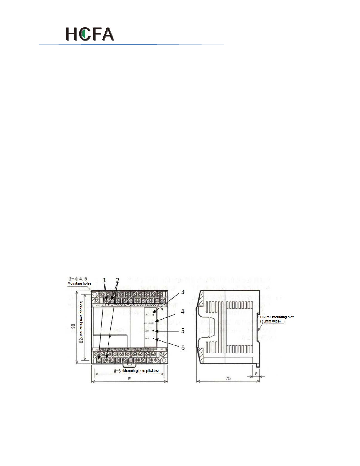
1.1 External Dimensions
1. 24V power supply terminal 2. 0V power supply terminal
3. A/D conversion indicator lamp 4. Bus power indicator lamp (LED)
5. 24V Power indicator lamp 6. D/A conversion indicator lamp

HCFA Corporation Limited
2
1.2 Connection with PLC
Various special function blocks controlled by FROM/TO instruction, such as analog input
units, high speed counting units, can be connected to TX2N programmable
controller(MPU) or the right of other expansion blocks or units. At most 8 special function
blocks can be connected to a MPU from No.0 to No.7 in sequence. As TX2N-4AD4DA is
the equivalent of 4AD, 4DA special function units(TX2N-4AD2DA is the equivalent of 4AD,
2DA special function units), if you want to connect these two special function units with
others at the same time, TX2N-4AD4DA(TX2N-4AD2DA)must be connected at last. At
most 6 special function blocks can be connected except TX2N-4AD4DA(TX2N-4AD2DA).
Please note that the serial number of AD follows the one of DA in TX2N-4AD4DA
(TX2N-4AD2DA).
For example, if 6 special function units has been connected before TX2N-4AD4DA
(TX2N-4AD2DA), DA number of TX2N-4AD4DA(TX2N-4AD2DA)is No.6, but AD
number is No.7.
TX2N-48MR-ES/UL TX2N-16EX TX2N-32ER TX2N-4AD-PT TX2N-4AD4DA
(TX2N-4AD2DA)
Special function Special function
blocks blocks
2. Wiring
1. The analog input and output are received through twisted pair shielded cable. This
cable should be wired away from power lines or any other lines which could induce
noise.
2. If a voltage ripple occurs during I/O, or there is electrically induced noise on the
external wiring, connect a smoothing capacitor of 0.1 to 0.47 µF, 25V.
3. If using current input, please connect the V+ and I+ terminal to each other.
4. If there is excessive voltage noise, connect the FG (frame ground) terminal with the
HCFA Corporation Limited
3
grounded terminal on 4AD.
5. Shorting voltage output terminal or connecting current output load to voltage output
terminal may damage the TX2N-4AD4DA(TX2N-4AD2DA)in D/A conversion.
6. Connect the ground terminal on the TX2N-4AD4DA (TX2N-4AD2DA)unit with the
grounded terminal on the main unit. Use 3-level grounding on the main unit, if
available.
3. Specification
3.1 Environment specification
Item Specification
Environment specifications Same as those on TX2N main unit
Dielectric withstand voltage 5000V AC, 1min (between all terminals and ground)
3.2 Power supply specification
Item Specification
Analog circuits 24V DC±10%,55mA (External power supply from the main unit)
Digital circuits 5V DC,30mA (Internal power supply from the main unit)
3.3 Performance specification
AD Analog Inputs
Items Voltage input Current input
Either voltage or current input can be selected with your choice of input terminal.
Up to four input points can be used at one time.
Analog input range DC -10V to 10V(Input resistance:200K
Ω)
DC -20mA to 20mA(Input resistance:250
Ω)
Digital output 12-bit conversion stored in 16-bit 2’s complement form Maximum value: +2047
Minimum value: -2048
Resolution 5mV(10V default range:1/2000) 20A(20mA default range:1/1000)
Overall accuracy ±1%(for the range of -10V to +10V) ±1%(for the range of -20mA to +20mA)
Conversion Speed 15ms/channel (Normal speed), 6ms/channel (High speed)
DA Analog output

HCFA Corporation Limited
4
Item Voltage output Current output
Analog output
range
DC -10V to 10V (External load resistance:
2KΩto 1MΩ)
DC 0mA to 20mA(External load resistance:500Ω)
Digital Input 16 bits, binary, with sign (Effective bits for numeric value:11 bits and sign bit (1 bit))
(Effective bits for numeric value: 11 bits and sign bit (1 bit)
Resolution 5mV(10V*1/2000) 20μA(20mA*1/1000)
Overall accuracy ±1%(for the range of -10V to +10V ) ±1% (for the range of -20mA to +20mA )
Conversion speed
TX2N-4AD4DA,DA has 4 channels(TX2N-4AD2DA ,DA has 2 channels)
2.1ms for each channel(Change in the number of channels used will not change the conversion speed)
Isolation
Photo-coupler isolation between analog and digital circuits.
DC/DC converter isolation of power from PLC main unit.
No isolation between analog channels
External power
supply
24V DC±10% 200mA
Number of
occupied I/O points
The analog block occupies 8 I/O points. (can be either inputs or outputs)
Power
consumption
5V, 30mA (Internal power supply from MPU or powered extension unit)
I/O Characteristics
(Default: Mode 0)
4. Allocation of buffer memory(BFM)
4.1 Allocation of AD buffer memory(BFM)
BFM Contents
*#0 Channel initialization Default = H0000
*#1 Channel 1 Contains the number of samples (1 to 4096) to be used for
an averaged result.
The default setting is 8- normal speed. High speed
operation can be selected with a value of 1.
*#2 Channel 2
*#3 Channel 3
*#4 Channel 4
#5 Channel 1 These buffer memories contain the averaged input values
for the number of samples entered for the channel in buffer
memories #1 to #4 respectively.
#6 Channel 2
#7 Channel 3

HCFA Corporation Limited
5
#8 Channel 4
#9 Channel 1 These buffer memories contain the present value currently
being read by each input channel.
#10 Channel 2
#11 Channel 3
#12 Channel 4
#13-#14 Reserved
#15 Selection of A/D conversion speed When set to 0, a normal speed is selected of 15ms/channel
When set to 1, a high speed is selected of 6ms/channel
●In buffer memory locations (BFMs) marked with an “*”, data can be written from the PLC
using the TO instruction.
●For buffer memories (BFMs) without “*” mark, data can be read by the PLC using the
FROM instruction.
●Before reading from the analog special function block, ensure that the appropriate
settings have been sent to the analog special function block. Otherwise, the previous
values held in the analog block will be used.
BFM b7 b6 b5 b4 b3 b2 b1 b0
#16-#19 Reserved
*#20 Reset to Defaults and Preset. Default = 0
*#21 Offset, Gain Adjust Prohibit. Default = (0, 1) Permit
*#22 Offset, Gain Adjust G4 O4 G3 O3 G2 O2 G1 O1
*#23 Offset Value Default =0
*#24 Gain Value Default =5,000
#25-#28 Reserved
#29 Error status
#30 Identification code K2010
#31 Cannot be used
●The buffer memory also gives a facility to adjust the offset and gain via software.
●Offset (intercept): The analog input value when the digital output becomes 0.
●Gain (slope): The analog input value when the digital output becomes +1000.
1) Channel selection
Channel selection is made by a 4 character HEX number HOOOO in buffer memory BFM
#0.
The least significant character controls channel 1 and the 4th character controls channel
4.
Setting of each character is as follows:
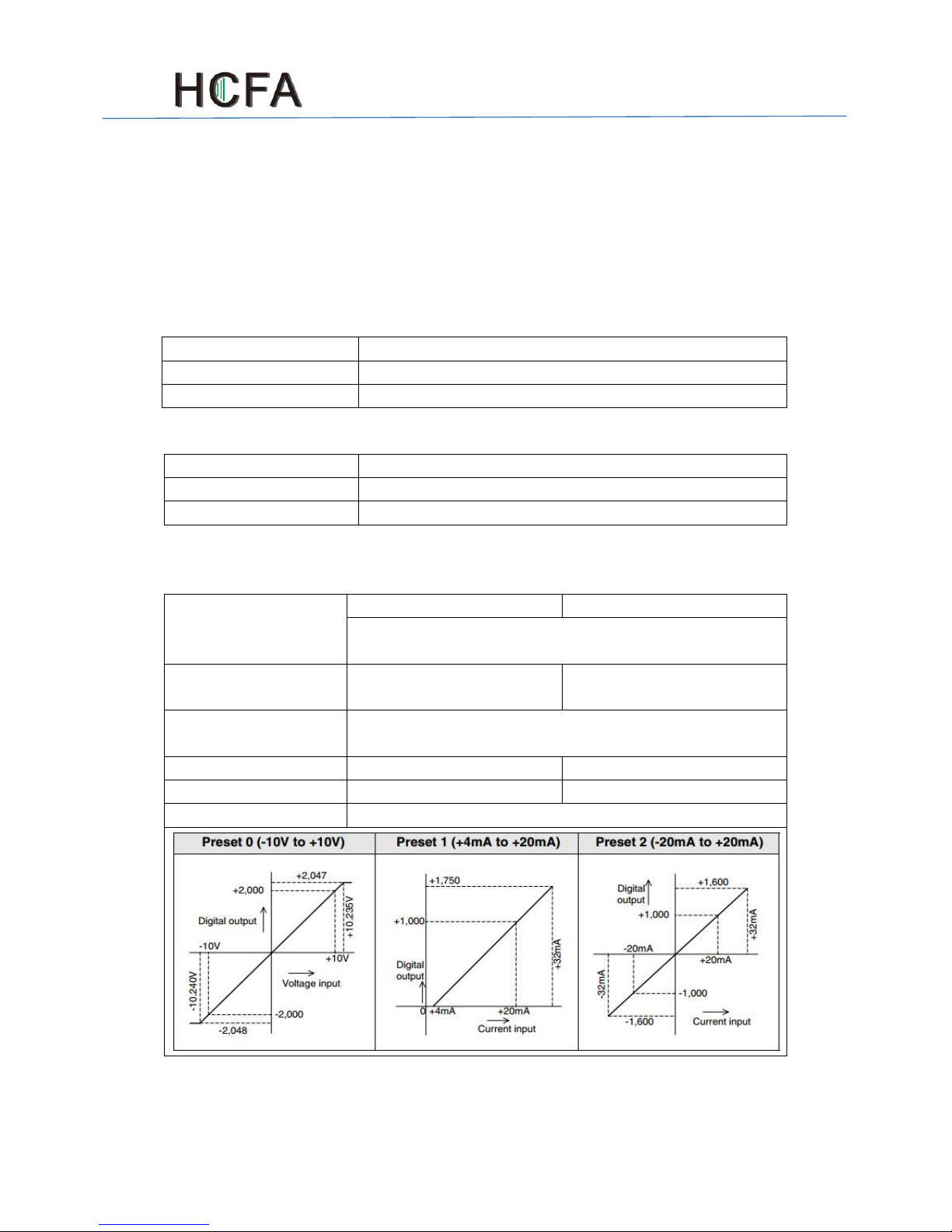
O = 0: Preset range (-10V to +10V) O = 2: Preset range (-20mA to +20mA)
O = 1: Preset range (+4mA to +20mA) O = 3: Channel OFF
Example: H3310
CH1 : Preset range (-10V to +10V)
CH2 : Preset range (+4mA to +20mA)
CH3, CH4: Channel OFF
2) Analog to digital conversion speed change
HCFA Corporation Limited
6
By writing 0 or 1 to BFM #15 of the AD Block, the speed at which A/D conversion is
performed can be changed.
3) Adjusting Gain and Offset values
a) When buffer memory BFM #20 is activated by setting it to K1, all settings within the
analog special function block are reset to their default settings.
b) If (b1, b0) of BFM #21 is set to (1,0), gain and offset adjustments are prohibited to
prevent inadvertent changes by the operator. In order to adjust the gain and offset values,
bits (b1, b0) must be set to (0,1). The default is (0,1)
c) Offset and gain values in BFM #23 and #24 are in units of mV or µA.
4) Status information BFM#29
Bit device of BFM#29 ON OFF
b0:Error When any of b1to b4 is ON, A/D conversion of
all the channels is stopped.
No error
b1:Offset/Gain error Offset/Gain data in the EEPROM
is corrupted or adjustment error.
Offset/Gain data normal
b2:Power source abnormality 24V DC power supply failure Power supply normal
b3:Hardware error A/D converter or other hardware failure Hardware normal
b10:Digital range error Digital output value is less than -2048 or more
than +2047
Digital output value is normal.
b11:Averaging error Number of averaging samples is 4097 or
more or 0 or less
Averaging is normal.
b12:Offset/gain adjust prohibit
Prohibit-(b1, b0) of BFM #21 is set to (1, 0) Permit-(b1, b0) of BFM #21 is set to
(1,0)
4.2 Allocation of DA buffer memory(BFM)
BFM Contents
W #0E Output mode selection. Factory setting H000
#1
#2
#3(Not used in TX2N-4AD2DA)
#4(Not used in TX2N-4AD2DA)
#5E Data holding mode. Factory setting H000
#6,#7 Reserved
1) [BFM #0] Output mode selection: The value of BFM #0 switches the analog output
between voltage and current on each channel. It takes the form of a 4 digit hexadecimal
number. The first digit will be the command for channel 1 (CH1), and the second digit for
channel 2 (CH2) etc. The numeric values of these four digits respectively represent the
following items:
O=0:Sets the voltage output mode (-10 V to +10 V)
H O O O O O=1:Sets the current output mode (+4mA to + 20mA)
CH4 CH3 CH2 CH1 O=2:Sets the current output mode(0mA to + 20mA)
HCFA Corporation Limited
7
Switching the output mode resets the I/O characteristics to the factory-default
characteristics.
2)Example: H2110
[BFM #1, #2, #3 and #4]: Output data channels CH1,CH2,CH3 and CH4
BFM #1: Output data of CH1(Initial value:0) BFM #2: Output data of CH2(Initial value:0)
BFM #3: Output data of CH3(Initial value:0) BFM #4: Output data of CH4(Initial value:0)
3) [BFM #5]: Data holding mode: While the programmable controller is in the STOP
mode, the last output value in the RUN mode will be held. To reset the value to the offset
value, write the hexadecimal value in BFM #5 as follows:
H O O O O O=1:Sets the current output mode(+4mA to + 20mA)
CH4 CH3 CH2 CH1 O=2:Sets the current output mode (0mA to + 20mA)
Example: H0011· · · · · · · · ·CH1 and CH2= Offset value CH3 and CH4= Output holding
In addition to above functions, the buffer memory can adjust the I/O characteristics of D/A
and report the D/A status to PLC.
BFM Description
W #8(E) Offset/Gain setting command of CH1, CH2, Initial value H0000
#9(E) Offset/Gain setting command of CH3, CH4, Initial value
H0000(Not used in TX2N-4AD2DA)
#10 Offset data CH1*1 Unit: mV or µA
Initial offset value:0
Initial gain value: +5,000
#11 Gain data CH1*2
#12 Offset data CH2*1
#13 Gain data CH2*2
#14(Not used in TX2N-4AD2DA) Offset data CH3*1
#15(Not used in TX2N-4AD2DA) Gain data CH3*2
#16(Not used in TX2N-4AD2DA) Offset data CH4*1
#17(Not used in TX2N-4AD2DA) Gain data CH4*2
#18,#19 Reserved
W #20(E) Initialize. initial value = 0
#21E I/O characteristics adjustment inhibit (Initial value 1)
#22-#28 Reserved
#29 Error status
#30 K3020 identification code
#31 Reserved
4) [BFM #8 and #9] Offset/gain setting command: Changes offset and gain values of
channels CH1 through CH4 by writing 1 to the corresponding Hex digits of BFM #8 or #9.
The current values will be valid until this command is output.
BFM #8 BFM #9 O=0:No changes done
H O O O O H O O O O O=1:Change data value
G2 O2 G1 O1 G4 O4 G3 O3
5) [BFM #10 to #17] Offset/ gain data: The offset and gain values are changed by writing

HCFA Corporation Limited
8
new data to BFM #10 through to #17. The units of the data to be written is mV or µA. The
data should be written and then BFM #8 and #9 set. Note that the data value will be
rounded down to the nearest 5mV or 20µA.
6) [BFM #20] Initialize: When K1 is written in BFM #20, all values will be initialized to the
factory-default. (Note that the BFM #20 data will override the BFM #21 data.) The initial
function is convenient when you have an error in adjustment.
7) [BFM #21] I/O characteristics adjustment inhibit: Setting BFM #21 to 2 inhibits user from
inadvertent adjustment of I/O characteristics. The adjustment inhibit function, once set,
will be valid until the Permit command (BFM#21=1)is set. The initial vale is 1(Permit).
The set value will be retained even after power-OFF.
8) [BFM #29] Error status: When error occurs, use the FROM command to read out the
details of error.
Bit Name Status when bit is set to “1”
(turned on)
Status when bit is set to “0”
(turned off)
b0 Error Error if any of b1 through b4 is turned on
No error
b1 O/G error Offset/gain data in EEPROM is abnormal
or a data setting error occurs
Offset/ gain data normal
b2 Power supply error 24V DC power failure Power supplied normally
b3 Hardware error Defective D/A converter or other
hardware
Non-defective hardware
b10 Range error The digital input or analog output value is
out of the specified range.
The input and output value is in the
specified range.
b12 G/O-adjustment prohibit
status
BFM#21 is not set to “1”. Adjustable status(BFM#21=1)
Bits b4 through b9, b11, b13 to b15 are not defined.
9) [BFM #30] The identification code for a special function block is read using the FROM
instruction. The identification code for 4DA is K3020. The main unit can use this facility in
the program to identify the special block before commencing any data transfers from and
to the special function block.
Note: BFM #’s marked E/(E).
●Values of BFM #0, #5, and #21, (marked E) are stored in the EEPROM memory of the
TX2N-4AD4DA. BFM #10 to #17 are copied to EEPROM when the gain/offset setting
command BFM #8, #9 is used. Also, BFM #20 causes the resetting of the EEPROM
memory. The EEPROM has a life of about 10,000 cycles (changes), so do not use
programs which frequently change these BFMs.
●A mode change of BFM #0 automatically involves a change of the corresponding offset
and gain values . Because of the time needed to write the new values to the internal
EEPROM memory, a delay of 3s is required between instructions changing BFM #0 and
instructions writing to the corresponding BFM #10 through BFM #17. Therefore, a delay
timer should be used before writing to BFM #10 through #17.
5 Defining gain and offset
5.1 AD gain and offset

HCFA Corporation Limited
9
Gain determines the angle or slope of Offset is the ‘position’ of calibration line,
calibration line, identified at a digital identified at a digital value of 0.
value of 1000.
a)Small gain value: Large steps in d)Negative offset
digital reading e)Zero offset: Default(0V or 4mA)
b)Zero gain value: Default(5V or 20mA) f)Positive offset
c)Big gain value: Small steps in
digital reading
5.2 DA gain and offset
The standard characteristics (factory default) are shown by the solid lines in the figure
below. These characteristics can be adjusted according to the conditions of the user’s
system.
Standard characteristics Standard characteristics Standard characteristics
of voltage output of current output of current output
(+4mA to +20mA) (0mA to +20mA)
● Gain value Analog output value when digital input is +1,000.
▲ Offset value Analog output value when digital input is 0.
When the slope of the I/O characteristic line is steep:
Slight changes to the digital input will greatly increase or reduce the analog output.
When the slope of the I/O characteristic line is gentle:
Slight changes to the digital input will not always change the analog output
Note that the resolution (minimum possible change of analog output) of the DA is fixed
6 Example program
6.1 Outline of FROM and TO commands

HCFA Corporation Limited
10
m1:Special unit or block number (K0 to K7, numbered from the MPU)
m2:Buffer memory head address (K0 to K31)
D*:Head device number of destination data. T, C, D, KnM, KnY, KnS, V, and Z can be
used to designate the head device. Each device number can be qualified using an index.
n:Number of transfer points (K1 to K32) (K1 to K16 for 32-bit command)
m1,m2,n:Same as above
S*:Head device number of source data. T, C, D, KnX, KnM, KnY, KnS, V, Z, K, and H can
be used to designate the head device. Each device number can be qualified using an
index.
When X010 and X011 are off, transfer will not be executed, therefore the destination data
value will not be changed.
6.2 AD Basic program
In the following example, CH1 and CH2 are used as voltage input. The TX2N-4AD4DA
AD block is connected at the position of special function block NO.1. The number of
averaged samples is set at 4 and data registers D0 and D1 of the main unit receive the
averaged digital data.
The ID code for the special function block at
position "1" is read from BFM #30 of that block and
stored at D4 in the main unit. This is compared
with K2010 to check that the block is AD block, if
OK M1 is turned ON.
The analog input channels (CH1, CH2) are setup
by writing H3300 to the BFM #0 of the AD block.
The number of average samples for CH1 and CH2
is set to 4 by writing 4 to BFM #1 and #2
respectively.
The operational status of 4AD is read from BFM
#29. If there are no errors in the operation of the
AD, then the averaged data BFM's are read.
In the case of this example BFM #5 and #6 are
read into the main unit and stored in D0 and D1.
These devices contain the averaged data for CH1
and CH2 respectively.
The push-button switch of PLC input terminal can adjust the gain/offset of 4AD in PLC
programming. The following is an example of changing the offset value on input channel
CH1 to 0V and the gain value to 2.5V. The 4AD block is in the position of block No.1.
HCFA Corporation Limited
11
Adjustment starts.
(H000)→BFM #0 (input channels selection)
Input instruction as shown in the left and PC run.
(K1)→BFM #21
BFM #21 (gain/offset prohibition) must be set to
permission with (b1, b0) = (0,1)
(K0)→BFM #22 (Offset/gain adjustment)
Reset adjustment bits.
(K0)→BFM #23 (Offset)
(K2500)→BFM #24(Gain)
(H003)→BFM #22(Offset/gain adjustment)
3= 0011 i. e. O1 = 1, G1 = 1
Channel 1 is adjusted.
End of adjustment.
(K1)→BFM #21(Offset/gain adjustment)
BFM#21 gain/offset prohibition
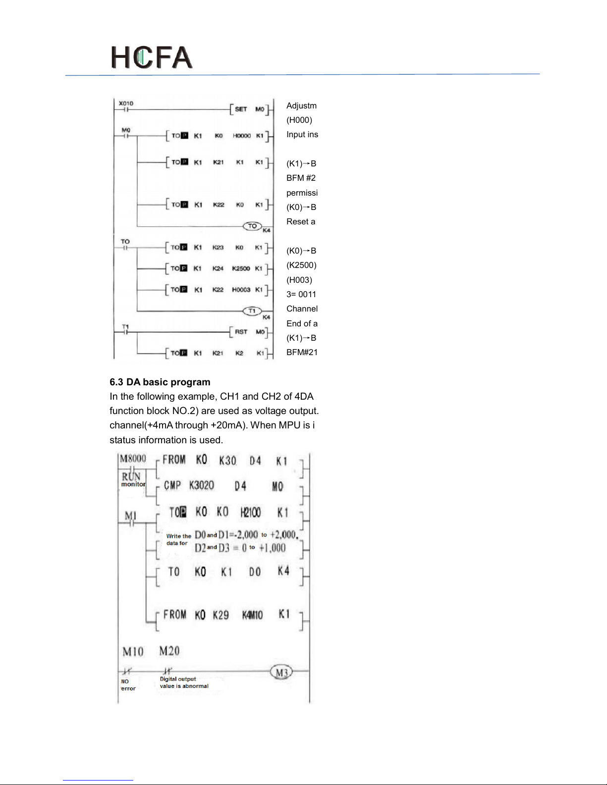
6.3 DA basic program
In the following example, CH1 and CH2 of 4DA block(connected in the position of special
function block NO.2) are used as voltage output. CH3 is used as current output
channel(+4mA through +20mA). When MPU is in STOP status, output reserved. Moreover,
status information is used.
The BFM#30 data(model code) in block NO.0
will be transferred to data register D4. M1 will
be turned on when the model code is set to
K3020.
H2100→BFM #0(NO.0 unit)
CH1 and CH2:voltage output; CH3:current
output (+4mA to +20mA); CH4:current
output(0mAto +20mA)
D0→BFM #1 (CH1 output) D1→BFM #2
(CH2
output)
D2→BFM #3 (CH3 output) D3→BFM #4(CH3
output)
BFM #29(b15 to b0) →(M25 to M10)
Reads out the status data.

HCFA Corporation Limited
12
Adjustment of I/O characteristics
To adjust the I/O characteristics, either the push-button switch connected to PLC input
terminal or forced ON/OFF function on programming panel can set offset/gain value in
4DA. To change the offset/gain, just change the conversion constant of 4DA. There is no
need to be adjusted by instrument measure analog output. However, programming is
needed in MPU. An example program for adjustment is shown below. The example shows
that for channel CH2 of 4DA block No.1, the offset value is changed to 7 mA, and the gain
value to 20 mA. Note that for CH1,CH3, and CH4, the standard voltage output
characteristics are set.
Operation start
(H0010)→BFM#0 Sets the mode of the output channel
(K1)→BFM#21 Permits adjustment of I/O
Characteristics
(K7000)→BFM#12
Sets the offset data. (Offset value: 7 mA)
(K20000)→BFM#13
Sets the gain data. (Gain value: 20 mA)
(H1100)→BFM#8
CH2 offset/gain setting command
Operation end
(K2)→BFM#21 Inhibits adjustment of I/O characteristics
After adjustment, the I/O characteristics will be as follows.
7 Diagnostics
If the TX2N-4AD4DA special function block does not operate properly, check the following
items.
1) Check the external wiring
2) Check status of the BUS LINK power indicator lamp (LED) of the TX2N-4AD4DA.
ON: The extension cable is properly connected.
OFF or Flash: Check the connection of extension cable. Also check the 5V power
supply capacity.
3) Check status of the 24 V power indicator lamp (LED) of the TX2N-4AD4DA.

HCFA Corporation Limited
13
ON: 24V DC is supplied.
OFF: Supply 24V DC(±10%)to the TX2N-4AD4DA
4) Check status of the A/D conversion indicator lamp (LED) of the TX2N-4AD4DA
ON: A/D conversion is proceeding normally.
Otherwise: Check buffer memory #29(error status). If any bits (b2 and b3) is ON,
then this is why A/D LED is OFF.
5) Check status of the D/A conversion indicator lamp(LED) of the TX2N-4AD4DA.
Flash : D/A conversion is normal.
ON or OFF: The ambient conditions are suitable for TX2N-4AD4DA, or the
TX2N-4AD4DA D/A is defective.
6) Check the external load resistance connected to each analog output terminals does not
exceed the capacity of TX2N-4AD4DA DA drive. (Voltage output : 2KΩto 1MΩ/current
output: 500Ω)
7) Check the output voltage or current value using a voltmeter or ammeter, and confirm
that the output meets the I/O characteristics. If the output does not meet the I/O
characteristics, adjust the offset and gain again.
Note: To test the withstand voltage of the TX2N-4AD4DA, connect all the terminals to the
grounding terminal.
This manual suits for next models
1
Popular Media Converter manuals by other brands


H&B
H&B TX-100 Installation and instruction manual

Bolin Technology
Bolin Technology D Series user manual

IFM Electronic
IFM Electronic Efector 400 RN30 Series Device manual

GRASS VALLEY
GRASS VALLEY KUDOSPRO ULC2000 user manual

Linear Technology
Linear Technology DC1523A Demo Manual

Lika
Lika ROTAPULS I28 Series quick start guide

Weidmuller
Weidmuller IE-MC-VL Series Hardware installation guide

Optical Systems Design
Optical Systems Design OSD2139 Series Operator's manual

Tema Telecomunicazioni
Tema Telecomunicazioni AD615/S product manual

KTI Networks
KTI Networks KGC-352 Series installation guide

Gira
Gira 0588 Series operating instructions

Lika
Lika SFA-5000-FD user guide