hilscher NXHX 52-JTAG Operating and installation instructions

Device Description
NXHX 52-JTAG
Development Board
Hilscher Gesellschaft für Systemautomation mbH
www.hilscher.com
DOC120809HW06EN | Revision 6 | English | 2013-11 | Released | Public

Table of Contents 2/59
NXHX 52-JTAG | Development Board
DOC120809HW06EN | Revision 6 | English | 2013-11 | Released | Public © Hilscher, 2012 - 2013
Table of Contents
1INTRODUCTION.........................................................................................................4
1.1 About This Manual......................................................................................................4
1.1.1 List of Revisions ...................................................................................................4
1.1.2 Conventions in this Manual ..................................................................................5
1.1.3 Reference to Hardware ........................................................................................5
1.2 Other Relevant Documentation ..................................................................................6
2DESCRIPTIONS AND DRAWINGS ............................................................................7
2.1 Description of the NXHX 52-JTAG .............................................................................7
2.2 Drawings.....................................................................................................................8
2.2.1 Block Diagram ......................................................................................................8
2.2.2 Printed Circuit Board ............................................................................................9
2.3 Operating Elements ..................................................................................................11
2.3.1 Push Buttons ......................................................................................................11
2.3.2 Switches .............................................................................................................12
2.4 Interfaces ..................................................................................................................17
2.4.1 Host Interface (X1) .............................................................................................17
2.4.2 Mini-B USB Connector (X3, 5 pin)......................................................................23
2.4.3 D-Sub Connector 9 pin (X7) ...............................................................................23
2.4.4 Micro SD Card Connector (X5) ..........................................................................24
2.4.5 Fieldbus Connector (X6 – 18 pin).......................................................................24
2.4.6 JTAG Connector (X4).........................................................................................25
2.4.7 2*RJ45 Ethernet Interface (X30) ........................................................................26
2.4.8 Power Supply +24 V (X100)...............................................................................26
2.5 LEDs .........................................................................................................................27
2.5.1 LED SYS (V1).....................................................................................................27
3USING THE DEBUGGER .........................................................................................28
4ACCESSORIES ........................................................................................................29
4.1 Devices for Host Interface ........................................................................................29
4.1.1 I/O Device at Host Interface (NXHX-IO).............................................................30
4.1.2 SDRAM Device at Host Interface (NXHX-SDR).................................................31
4.1.3 PHY and Serial Dual-Port Memory Device at Host Interface (NXHX-PHY).......32
4.1.4 PHY and SDR Memory Device at Host Interface (NXHX-PHYSDR) .................34
4.1.5 Parallel Dual-Port Memory at Host Interface (NXPCA-PCI)...............................35
4.1.6 Using NXHX 6-RE as Extension Bus at Host Interface......................................35
4.1.7 Accessory Cables and Connectors for Host Interface .......................................36
4.2 Fieldbus and Serial Adapters/Interfaces...................................................................37
4.2.1 NXHX-DP ...........................................................................................................37
4.2.2 NXHX-CO ...........................................................................................................38
4.2.3 NXHX-DN ...........................................................................................................38
4.2.4 NXHX-RS ...........................................................................................................39

Table of Contents 3/59
NXHX 52-JTAG | Development Board
DOC120809HW06EN | Revision 6 | English | 2013-11 | Released | Public © Hilscher, 2012 - 2013
4.2.5 NXHX-CC ...........................................................................................................39
4.3 NXAC-Power ............................................................................................................40
5REFERENCE ............................................................................................................41
5.1 Schematics ...............................................................................................................41
5.2 Bill of Materials .........................................................................................................50
5.2.1 NXHX 52-JTAG ..................................................................................................50
5.2.2 NXHX-IO.............................................................................................................52
5.2.3 NXHX-SDR.........................................................................................................52
5.2.4 NXHX-PHY .........................................................................................................53
5.2.5 NXHX-PHYSDR .................................................................................................54
6TECHNICAL DATA ...................................................................................................55
6.1 NXHX 52-JTAG ........................................................................................................55
7APPENDIX ................................................................................................................56
7.1 Matrix Label ..............................................................................................................56
7.2 List of Figures ...........................................................................................................57
7.3 List of Tables ............................................................................................................58
7.4 Contacts....................................................................................................................59

Introduction 4/59
NXHX 52-JTAG | Development Board
DOC120809HW06EN | Revision 6 | English | 2013-11 | Released | Public © Hilscher, 2012 - 2013
1 Introduction
1.1 About This Manual
This manual describes the NXHX 52-JTAG development board.
1.1.1 List of Revisions
Index Date Chapter Revision
1 2013-02-20 All Created
2 2013-03-21 2.3.2.1 Description of Host Interface Mode revised
3 2013-07-08 4.1.7 Section Accessory Cables and Connectors
for Host Interface added.
4 2013-07-16
2.3.2.1
2.3.2.2
4.1
Section Configuration Boot Strap Options -
Switch (S1) revised.
Section Configuration Host Mode - Switch
(S2) revised.
Section Devices for Host Interface revised
(formerly section Host Interfaces)
5 2013-10-28
5.1
1.2
4.1.5
Schematics updated for hardware revision 2
of NXHX board.
Section Other Relevant Documentation
added.
Descriptions of switch settings for operating
the NXHX board with NXPCA-PCI board
revised.
6 2013-11-13 5.1
2.3.2.2
4.1.5
Schematics updated for hardware revision 3
of NXHX board.
Descriptions of settings of Switch S2
(configuration host mode) updated according
to hardware revision 3 of NXHX board.
Descriptions of switch settings for operating
the NXHX board with NXPCA-PCI board
updated according to hardware revision 3 of
NXHX board.
Table 1: List of Revisions
Introduction 5/59
NXHX 52-JTAG | Development Board
DOC120809HW06EN | Revision 6 | English | 2013-11 | Released | Public © Hilscher, 2012 - 2013
1.1.2 Conventions in this Manual
Notes are marked as follows:
Important: <important note>
Note: <note>
<note, where to find further information>
Positions in Figures
The Positions , , ... or , , ... or , , ... refer to the
figure used in that section. If the numbers reference to a section outside the
current section then a cross reference to that section and figure is
indicated.
1.1.3 Reference to Hardware
Hardware Revision Part Number
NXHX 52-JTAG 3 7773.300
Table 2: Reference to Hardware

Introduction 6/59
NXHX 52-JTAG | Development Board
DOC120809HW06EN | Revision 6 | English | 2013-11 | Released | Public © Hilscher, 2012 - 2013
1.2 Other Relevant Documentation
Besides this device description, the following documents are also relevant
for the user of the NXHX 52-JTAG development board:
Manual Contents Document Name
NXHX 52-JTAG
Getting Started Guide
Describes typical use cases of the
NXHX 52-JTAG Development Board.
NXHX 52-JTAG Getting Started GS XX EN.pdf
Migration Guide
netX 50 to netX 51/52
Describes the differences between
the netX 50 and netX 51/52.
Migration_netX50_to_netX5152_MG03EN.pdf
Programming
Reference Guide netX
51/52
Describes all available registers of
the netX 52.
netX 51 52 Programming Reference Guide PRG
xx EN.pdf
User Manual NXPCA-
PCI
Describes the coupling of the parallel
dual-port memory with a PC.
User Manual NXPCA-PCI_Rev_2_EN.pdf
Table 3: Additional Documentation

Descriptions and Drawings 7/59
NXHX 52-JTAG | Development Board
DOC120809HW06EN | Revision 6 | English | 2013-11 | Released | Public © Hilscher, 2012 - 2013
2 Descriptions and Drawings
2.1 Description of the NXHX 52-JTAG
The NXHX 52-JTAG is a development board for netX 52 and has the
following functions:
Host interface, usable in different interface modes: 8/16/32 bit parallel
dual-port memory, 16 bit TI multiplexed parallel dual-port memory, serial
dual-port memory (SPI Slave), MII and PIO.
2-port RJ45 Ethernet interface
D-Sub Serial RS-232 interface
DIP switch to configure boot mode and host interface mode
USB interface for diagnostic
MMIO signals and I2C interface
CAN interface
JTAG interface for debugging
System status and communication status LEDs
Micro SD card connector
Quad SPI flash for Fast Start-Up feature of PROFINET IO Device
Configuration of different boot options and host interface modes
1 bit “general purpose” IO with LED and push button

Descriptions and Drawings 8/59
NXHX 52-JTAG | Development Board
DOC120809HW06EN | Revision 6 | English | 2013-11 | Released | Public © Hilscher, 2012 - 2013
2.2 Drawings
2.2.1 Block Diagram
Figure 1: NXHX 52-JTAG Block Diagram

Descriptions and Drawings 9/59
NXHX 52-JTAG | Development Board
DOC120809HW06EN | Revision 6 | English | 2013-11 | Released | Public © Hilscher, 2012 - 2013
2.2.2 Printed Circuit Board
Figure 2: NXHX 52-JTAG Printed Circuit Board
No. in
figure Name Description For details see section Page
X1 Host interface Host Interface (X1) 17
X30 RJ45 Connector Ethernet interface CH1 2*RJ45 Ethernet Interface (X30) 26
Matrix-Label Matrix Label 56
X30 RJ45 Connector Ethernet interface CH0 2*RJ45 Ethernet Interface (X30) 26
V1 System status LED (yellow / green) LED SYS (V1) 27
V30 Communication status LED 0 (green / red) LEDs 27
V31 Communication status LED 1 (green / red) LEDs 27
T2 GPIO input, MMIO08 GPIO Input (T2) 11
V3 GPIO output LED (yellow), MMIO09 LEDs 27
X6 MMIO, SPI, I2C, CAN Fieldbus Connector (X6 – 18 pin) 24
S3 RS-Mode Configuration RS Mode - Switch (S3) 15
X7 9 pin D-Sub connector RS-232 D-Sub Connector 9 pin (X7) 23
- Device name - -
X5 micro SD Card connector Micro SD Card Connector (X5) 24
- micro SD Card (not part of delivery) formatting:
FAT, max. 2 GByte Micro SD Card Connector (X5) 24
X100 Power supply socket Power Supply +24 V (X100) 26
Descriptions and Drawings 10/59
NXHX 52-JTAG | Development Board
DOC120809HW06EN | Revision 6 | English | 2013-11 | Released | Public © Hilscher, 2012 - 2013
No. in
figure Name Description For details see section Page
- Drilling for attaching Fieldbus interface to X6 - -
S1 Boot strap options Configuration Boot Strap Options -
Switch (S1) 12
T1 Power On Reset Reset (T1) 11
X3 Mini-B USB connector Mini-B USB Connector (X3, 5 pin) 23
X4 JTAG Interface, plug connector 20 pin JTAG Connector (X4) 25
S2 Host Interface Mode / Boot Mode Configuration Host Mode - Switch
(S2) 15
Table 4: List of Positions on Printed Circuit Board

Descriptions and Drawings 11/59
NXHX 52-JTAG | Development Board
DOC120809HW06EN | Revision 6 | English | 2013-11 | Released | Public © Hilscher, 2012 - 2013
2.3 Operating Elements
2.3.1 Push Buttons
2.3.1.1 Reset (T1)
T1 Function
When button is pushed, system initiates power-on reset.
Table 5: Push Button T1
Position in Figure 2: NXHX 52-JTAG Printed Circuit Board on page 9.
2.3.1.2 GPIO Input (T2)
T2 Function
General purpose input with push button.
Parallel to SD card detect switch. Switches high signal to
MMIO09.
Table 6: Push Button T2
Position in Figure 2: NXHX 52-JTAG Printed Circuit Board on page 9.
Descriptions and Drawings 12/59
NXHX 52-JTAG | Development Board
DOC120809HW06EN | Revision 6 | English | 2013-11 | Released | Public © Hilscher, 2012 - 2013
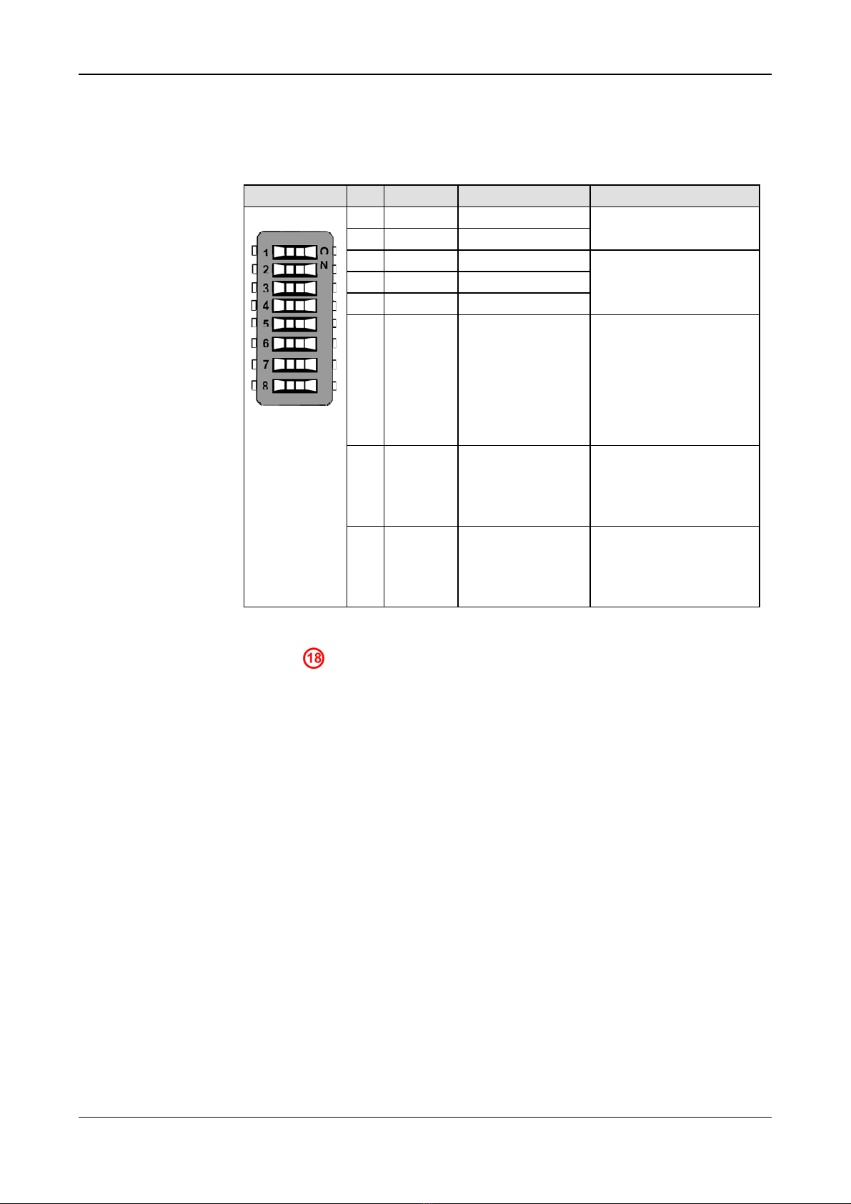
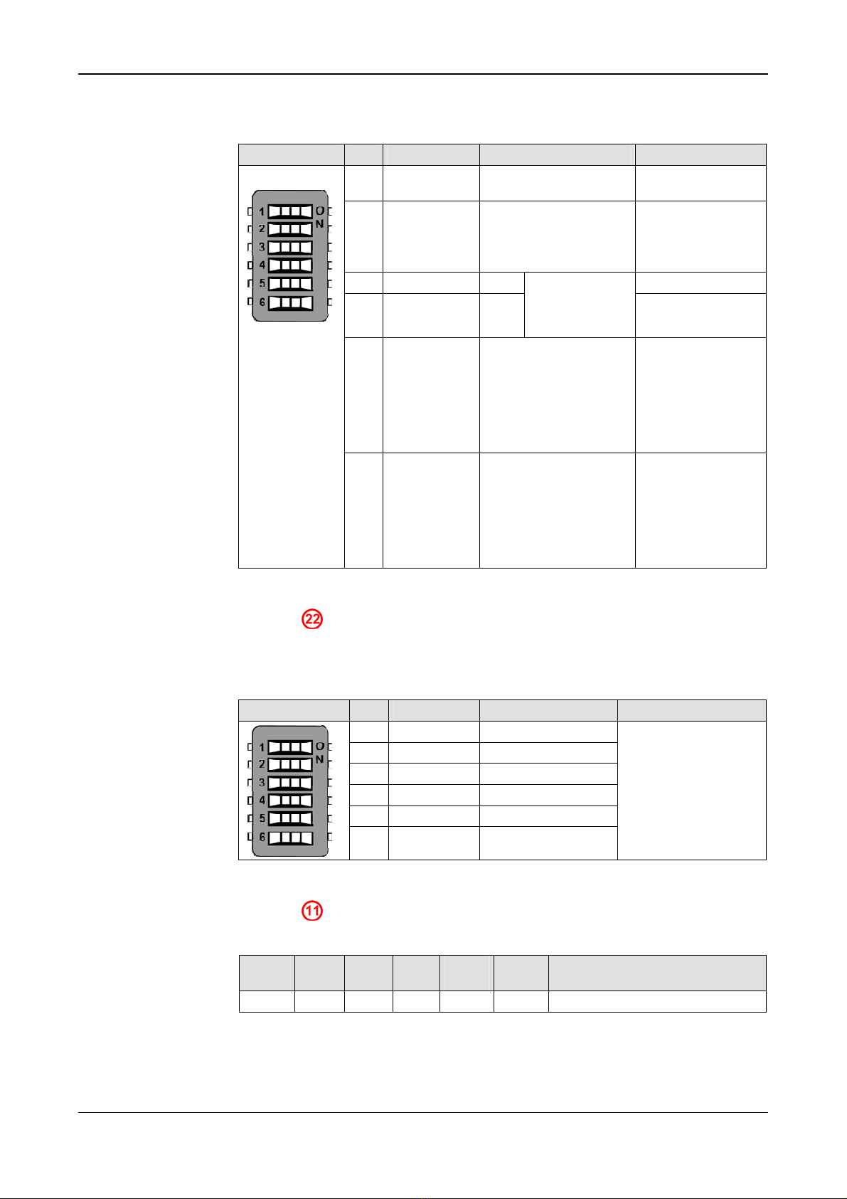
2.3.2 Switches
2.3.2.1 Configuration Boot Strap Options - Switch (S1)
Boot strap options.
S1 SW Signal Connect to Functions
1 RDY# with 390 Ωto GND
2 RUN# with 390 Ωto GND
Boot mode
3 SPI_MOSI with 1.5 kΩto +3.3 V
4 SPI_CLK with 1.5 kΩto +3.3 V
5 SPI_MISO with 1.5 kΩto +3.3 V
Host Interface Mode
6 RUN# SDA of Security
Memory
Access to Security Memory:
ON = Enable
OFF = Disable
Note that the Security
Memory will only be
accessed if SW 1 and SW 2
(RDY# and RUN#) are set
to OFF!
7 MMIO08
X1.4
DPM_SIRQ#
If in extension bus mode
with DPM connected at host
interface:
ON = Connect MMIO08 to
DPM_SIRQ#
8 MMIO03
X1.11
DPM_DIRQ#
If in extension bus mode
with DPM connected at host
interface:
ON = Connect MMIO03 to
DPM_DIRQ#
Table 7: Configuration - Switch S1, Boot Strap Options
Position in Figure 2: NXHX 52-JTAG Printed Circuit Board on page 9.
The boot mode and the host interface mode are evaluated by the ROM
loader during boot.
Boot Mode
If S1.6 is ON and S1.1 and S1.2 are both set to OFF, the boot mode is read
from the security memory. The boot mode defined in the security memory is
as follows:
1. Boot from parallel FLASH at host interface, if bootloader code is found.
2. Boot from serial FLASH using Quad SPI and XIP (CS0), if bootloader
code is found.
3. Boot from SD card, if bootloader code is found.

Descriptions and Drawings 13/59
NXHX 52-JTAG | Development Board
DOC120809HW06EN | Revision 6 | English | 2013-11 | Released | Public © Hilscher, 2012 - 2013
If S1.6 is set to OFF or one or both of the S1.1 and S1.2 switches are set to
ON, the security memory will not be accessed. In this case, the boot mode
is determined by S1.1 and S1.2 as described in the following table:
No. Selection S1.1 S1.2 Boot Sequence
1 FLASH/Ethernet boot mode off off 1. Boot from parallel FLASH at host interface,
if bootloader code is found.
2. Boot from serial FLASH using Quad SPI
and XIP (CS0), if bootloader code is found.
3. Boot from Ethernet CH_A with DHCP and
TFTP, if bootloader code is found.
2 Serial – UART0 and USB boot mode on off Boot from serial interface: UART0 or USB.
3 FLASH/Dual-Port Memory boot
mode
off on 1. Boot from serial FLASH using Quad SPI
and XIP (CS0), if bootloader code is found.
2. Boot from dual-port memory. Select the host
interface mode with S1.3, S1.4 and S1.5
(described in Table 9 on page 14).
4 FLASH boot mode on on 1. Boot from parallel FLASH at host interface,
if bootloader code is found.
2. Boot from serial FLASH using Quad SPI
and XIP (CS0), if bootloader code is found.
Table 8: Boot Mode Settings
Note: If you use boot mode 1, 2 or 4, set host interface mode to “Ignore
host interface during boot” (see subsequent table).
Descriptions and Drawings 14/59
NXHX 52-JTAG | Development Board
DOC120809HW06EN | Revision 6 | English | 2013-11 | Released | Public © Hilscher, 2012 - 2013
Host Interface Mode
The Host Interface Mode is selected by the signals SPI_MOSI (S1.3),
SPI_CLK (S1.4) and SPI_MISO (S1.5). The ROM code reads these signals
and uses them to initialize the Host Interface during the boot process. This
means that depending on the selected mode, signals are driven actively
from netX or from the host.
To select the right Host Interface Mode consider the following:
1. specify the device that is physically connected to the host interface of
the netX and
2. specify which device netX has to use as source or destination device
during boot.
S1.3 S1.4 S1.5 Description Usable
with boot
mode No.
Note
netX boots from the connected memory
off off off Ignore host interface during boot
Use this setting, if netX should not boot from
the host interface.
1, 2, 4
-
off off on SDRAM 16 bit data / 4 MByte
Use this setting, when using the module
NXHX-PHYSDR. SDRAM is used as
destination device.
1, 3, 4
off on off SRAM 16 bit data / 4 MB
Use this setting, if you have connected
parallel Flash (CS0) at the host interface and
netX has to boot from it. The parallel Flash is
used as source device.
- or -
Use this setting, if you have connected static
RAM (CS0, 1, 2 or 3) at the host interface.
The static RAM is used as destination device.
1, 4
on off on SDRAM 32 bit data / 4 MB
Use this setting, when using the module
NXHX-SDR. SDRAM is used as destination
device.
1, 3, 4
Using this mode requires
additionally that the
destination device in the boot
block of the bootable image is
set properly.
Host CPU supported: Host CPU boots netX via Dual-Port Memory
off on on Serial dual-port memory (SPM) mode
Use this setting, if you have connected a
serial dual-port memory at the host interface
and netX has to boot from it. The serial dual-
port memory is used as source device.
3
on off off Parallel dual-port memory (DPM) 8 bit data
/ 2 KB
Use this setting, if you have connected a
parallel dual-port memory at the host interface
and netX has to boot from it. The parallel
dual-port memory is used as source device.
3
on on on Parallel dual-port memory (DPM) 8 bit data
/ 64 Kbyte
Use this setting, if you have connected a
parallel dual-port memory at the host interface
and netX has to boot from it. The parallel
dual-port memory is used as source device.
3
The dual-port memory is used
for booting netX. The netX
waits for the Host CPU, which
has to transfer the bootable
image (e. g. Second Stage
Bootloader). Therefore the
Host CPU has to use the
mailboxes of netX for
transferring the boot code.
Reserved
on on off Do not use this setting! - -
Table 9: Host Interface Mode at X1 (Settings)
Descriptions and Drawings 15/59
NXHX 52-JTAG | Development Board
DOC120809HW06EN | Revision 6 | English | 2013-11 | Released | Public © Hilscher, 2012 - 2013
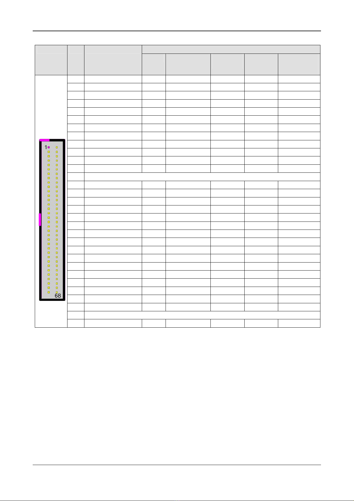
2.3.2.2 Configuration Host Mode - Switch (S2)
Host Mode
S2 SW Signal Connected to Description
1 DPM_DIRQ# 2.2 kΩto GND ON = SPI
OFF = DPM
2 DPM_SIRQ# 2.2 kΩto GND If S2.1 = OFF
(DPM):
ON = 8 Bit
OFF = 16 Bit
3 SD_RAS# X1.7 ON if SDRAM
4 DPM_RESn X1.7
Note!
Only one switch
is allowed to be
in ON position!
ON if DPM
5 DPM_DIRQ# X1.11 // S1.8 If in DPM mode, set
SW 5 to ON.
If in Extension Bus
Mode with DPM
connected at host
interface, set SW 5
to OFF.
6 DPM_SIRQ# X1.4 // S1.7 If in DPM mode, set
SW 6 to ON.
If in Extension Bus
Mode with DPM
connected at host
interface, set SW 6
to OFF.
Table 10: Configuration - Switch S2, Host Mode
Position in Figure 2: NXHX 52-JTAG Printed Circuit Board on page 9.
2.3.2.3 Configuration RS Mode - Switch (S3)
RS Mode, at connector X7
S3 SW Signal Connected to Description
1 LB to + 3.3 V
2 H / F to + 3.3 V
3 - to + 3.3 V
4 232 to + 3.3 V
5 RXEN to + 3.3 V
6 DXEN to + 3.3 V
Function
see subsequent table
Sets the function of X7
Table 11: Configuration - Switch S3, RS Mode
Position in Figure 2: NXHX 52-JTAG Printed Circuit Board on page 9.
S3.1
LB S3.2
H/F S3.3
S3.4
S3.5
RXEN S3.6
DXEN Function
off X X off off on RS-232
Table 12: Configuration - Switch S3, RS Mode
X = any position


Descriptions and Drawings 17/59
NXHX 52-JTAG | Development Board
DOC120809HW06EN | Revision 6 | English | 2013-11 | Released | Public © Hilscher, 2012 - 2013
2.4 Interfaces
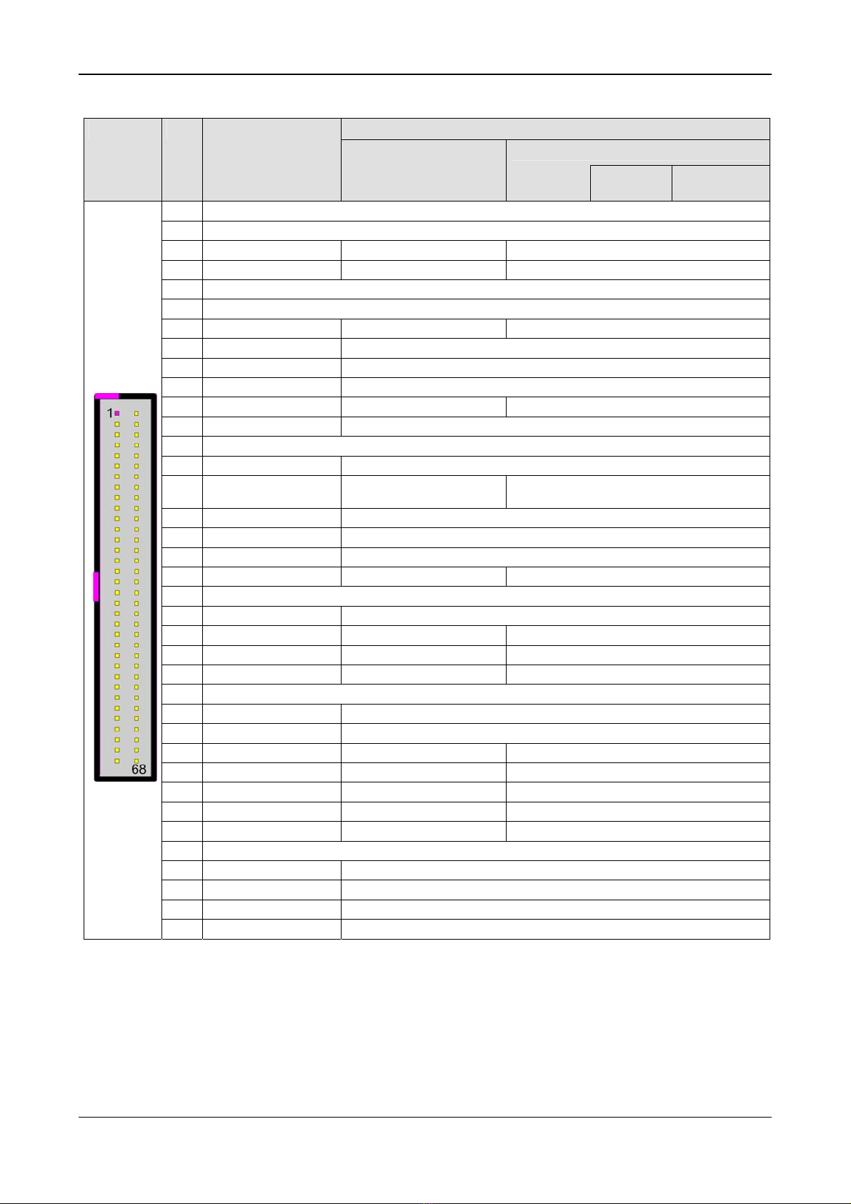
2.4.1 Host Interface (X1)
Position in Figure 2: NXHX 52-JTAG Printed Circuit Board on page 9.
2.4.1.1 DPM and SDRAM Modes
Host Interface ModesX1 Pin Signal
PIO SDRAM
32 Bit DPM
32 Bit DPM
8/16 Bit DPM
16 Bit
TI Multiplex
1 +3V3
2 GND
3 PIO59 SDRAM_CASn DPM_A17 DPM_A17
4 DPM_SIRQ# SDRAM_CLK
5 GND
6 RSTOUTn
7 DPM_RESn or PIO58 SDRAM_RASn DPM_A16
8 PIO85 SDRAM_D15 DPM_D31
9 PIO40 SDRAM_D10 DPM_D18
10 PIO36 SDRAM_D8 DPM_D16
11 MMIO03 or PIO47 DPM_DIRQ DPM_DIRQ
12 PIO46 SDRAM_CKE DPM_RDY DPM_RDY DPM_RDY
13 GND
14 PIO52 SDRAM_DQM2n DPM_RDn DPM_RDn DPM_RDn
15 PIO44 SDRAM_DQM3n DPM_BE3n
16 PIO45 SDRAM_WEn DPM_WRn DPM_WRn DPM_WRn
17 WDG_
ACT
SDRAM_D11 DPM_D19
18 PIO35 SDRAM_D9 DPM_D17
19 PIO43 SDRAM_DQM1n DPM_BE1n DPM_BHEn DPM_BE1n
20 GND
21 PIO84 SDRAM_D14 DPM_D30
22 PIO79 DPM_D28 DPM_D28
23 PIO80 DPM_D29 DPM_D29
24 PIO51 SDRAM_CSn DPM_CSn DPM_CSn DPM_CSn
25 GND
26 PIO72 SDRAM_D13 DPM_D27
27 PIO71 SDRAM_D12 DPM_D26
28 PIO68 SDRAM_D25 DPM_D25
29 PIO67 SDRAM_D24 DPM_D24
30 PIO63 SDRAM_D23 DPM_D23
31 PIO62 SDRAM_D22 DPM_D22
32 PIO59 SDRAM_D21 DPM_D21
33 GND
34 PIO55 SDRAM_BA1 DPM_A15 DPM_A15
35 PIO54 SDRAM_BA0 DPM_A14 DPM_A14
36 PIO48 SDRAM_DQM0n DPM_A13 DPM_A13
37 PIO49 SDRAM_A12 DPM_A12 DPM_A12
Table 13: Pin Assignment X1 Host Interface DPM and SDRAM Modes (Part 1)
Descriptions and Drawings 18/59
NXHX 52-JTAG | Development Board
DOC120809HW06EN | Revision 6 | English | 2013-11 | Released | Public © Hilscher, 2012 - 2013
Host Interface ModesX1 Pin Signal
PIO SDRAM
32 Bit DPM
32 Bit DPM
8/16 Bit DPM
16 Bit
TI Multiplex
38 PIO50 SDRAM_A11 DPM_A11 DPM_A11
39 PIO53 SDRAM_A10 DPM_A10 DPM_A10
40 PIO56 SDRAM_A9 DPM_A9 DPM_A9
41 PIO57 SDRAM_A8 DPM_A8 DPM_A8
42 PIO60 SDRAM_A7 DPM_A7 DPM_A7
43 PIO61 SDRAM_A6 DPM_A6 DPM_A6
44 PIO64 SDRAM_A5 DPM_A5 DPM_A5
45 PIO65 SDRAM_A4 DPM_A4 DPM_A4
46 PIO66 SDRAM_A3 DPM_A3 DPM_A3
47 PIO69 SDRAM_A2 DPM_A2 DPM_A2
48 PIO70 SDRAM_A1 DPM_BE2n DPM_A1 DPM_ADV
49 PIO73 SDRAM_A0 DPM_BE0n DPM_A0 DPM_BE0n
50 GND
51 PIO41 SDRAM_D31 DPM_D15 DPM_D15 DPM_AD15
52 PIO42 SDRAM_D30 DPM_D14 DPM_D14 DPM_AD14
53 PIO37 SDRAM_D27 DPM_D13 DPM_D13 DPM_AD13
54 PIO38 SDRAM_D26 DPM_D12 DPM_D12 DPM_AD12
55 PIO39 SDRAM_D19 DPM_D11 DPM_D11 DPM_AD11
56 PIO33 SDRAM_D18 DPM_D10 DPM_D10 DPM_AD10
57 PIO34 SDRAM_D17 DPM_D9 DPM_D9 DPM_AD9
58 PIO32 SDRAM_D16 DPM_D8 DPM_D8 DPM_AD8
59 PIO74 SDRAM_D7 DPM_D7 DPM_D7 DPM_AD7
60 PIO75 SDRAM_D6 DPM_D6 DPM_D6 DPM_AD6
61 PIO76 SDRAM_D5 DPM_D5 DPM_D5 DPM_AD5
62 PIO77 SDRAM_D4 DPM_D4 DPM_D4 DPM_AD4
63 PIO78 SDRAM_D3 DPM_D3 DPM_D3 DPM_AD3
64 PIO81 SDRAM_D2 DPM_D2 DPM_D2 DPM_AD2
65 PIO82 SDRAM_D1 DPM_D1 DPM_D1 DPM_AD1
66 PIO83 SDRAM_D0 DPM_D0 DPM_D0 DPM_AD0
67 +3V3
68 PIO58 SDRAM_D20 DPM_D20
Table 14: Pin Assignment X1 Host Interface DPM and SDRAM Modes (Part 2)
Descriptions and Drawings 19/59
NXHX 52-JTAG | Development Board
DOC120809HW06EN | Revision 6 | English | 2013-11 | Released | Public © Hilscher, 2012 - 2013
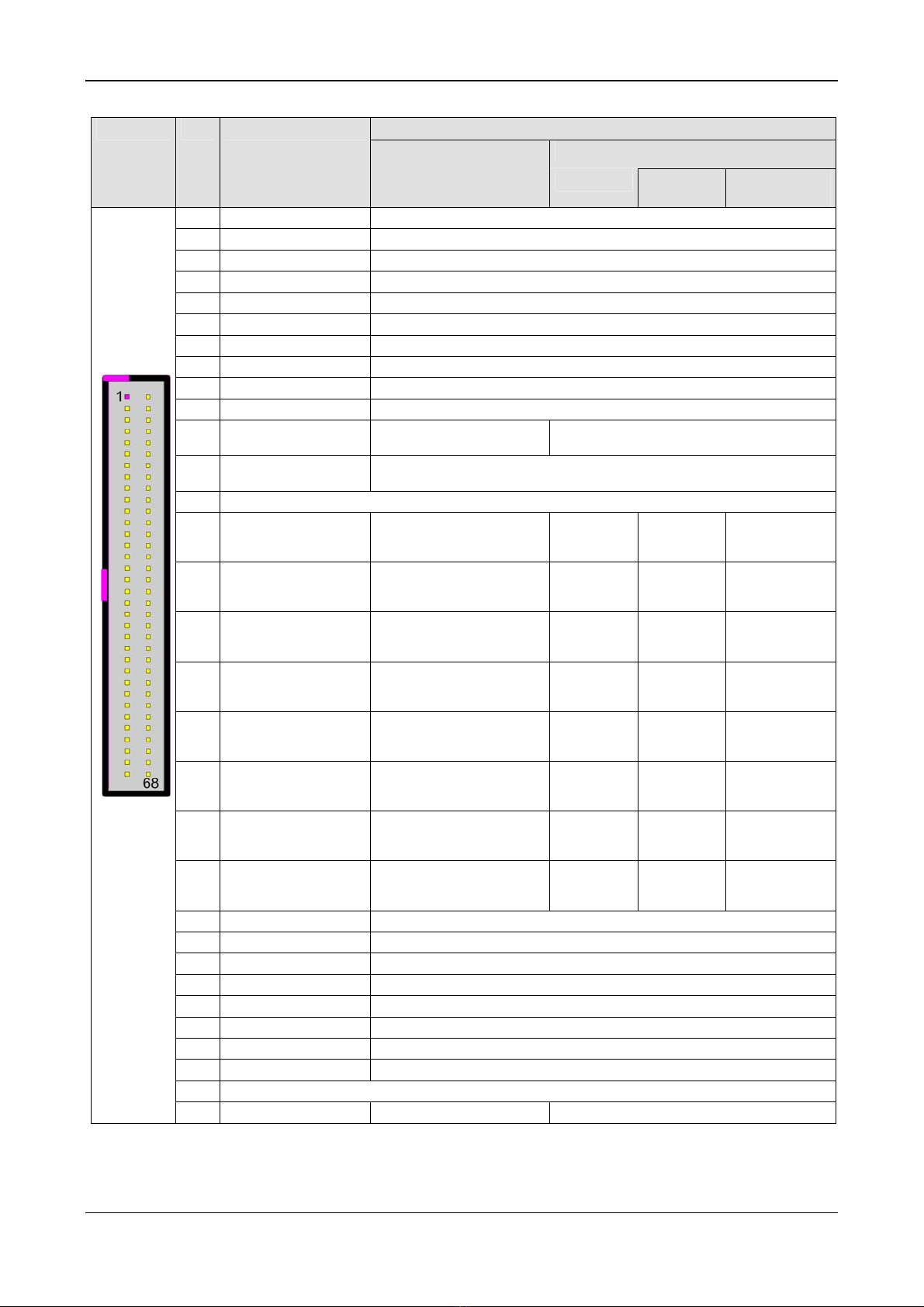
2.4.1.2 Extension Bus Modes
Host Interface Modes
Extension Bus 8/16 Bit Mode
X1 Pin Signal
Extension Bus 8/16/32
Bit Mode SPM
Extension MMIO
Extension
1 +3V3
2 GND
3 EXT_A17 EXT_A23
4 DPM_SIRQ#
5 GND
6 RSTOUTn
7 DPM_RESn or EXT_A16 EXT_A22
8 EXT_D15
9 EXT_D10
10 EXT_D8
11 MMIO03 or EXT_CS1n EXT_INTn
12 EXT_BUSYn
13 GND
14 EXT_RDn
15 EXT_BE3n EXT_CS3n
EXT_A24
16 EXT_WRn
17 EXT_D11
18 EXT_D9
19 EXT_BE1n EXT_BHEn
20 GND
21 EXT_D14
22 EXT_D28 EXT_CS2n
23 EXT_D29 EXT_CS1n
24 EXT_CS0n EXT_CS0n
25 GND
26 EXT_D13
27 EXT_D12
28 EXT_D25 EXT_A21
29 EXT_D24 EXT_A20
30 EXT_D23 EXT_A19
31 EXT_D22 EXT_A18
32 EXT_D21 EXT_A17
33 GND
34 EXT_A15
35 EXT_A14
36 EXT_A13
37 EXT_A12
Table 15: Pin Assignment X1 Host Interface Extension Bus Modes (Part 1)
Descriptions and Drawings 20/59
NXHX 52-JTAG | Development Board
DOC120809HW06EN | Revision 6 | English | 2013-11 | Released | Public © Hilscher, 2012 - 2013
Host Interface Modes
Extension Bus 8/16 Bit Mode
X1 Pin Signal
Extension Bus 8/16/32
Bit Mode SPM
Extension MMIO
Extension
38 EXT_A11
39 EXT_A10
40 EXT_A9
41 EXT_A8
42 EXT_A7
43 EXT_A6
44 EXT_A5
45 EXT_A4
46 EXT_A3
47 EXT_A2
48 EXT_A1
EXT_BE2n
EXT_A1
49 EXT_A0
EXT_BE0n
50 GND
51 EXT_D31 extendible
by SPM or
MMIO
SPM_SIO3 MMIO47
52 EXT_D30 extendible
by SPM or
MMIO
SPM_SIO2 MMIO46
53 EXT_D27 extendible
by SPM or
MMIO
SPM_SIRQ MMIO45
54 EXT_D26 extendible
by SPM or
MMIO
SPM_DIRQ MMIO44
55 EXT_D19 extendible
by SPM or
MMIO
SPM_CLK MMIO43
56 EXT_D18 extendible
by SPM or
MMIO
SPM_CSn MMIO42
57 EXT_D17 extendible
by SPM or
MMIO
SPM_MOSI MMIO41
58 EXT_D16 extendible
by SPM or
MMIO
SPM_MISO MMIO40
59 EXT_D7
60 EXT_D6
61 EXT_D5
62 EXT_D4
63 EXT_D3
64 EXT_D2
65 EXT_D1
66 EXT_D0
67 +3V3
68 EXT_D20 EXT_A16
Table 16: Pin Assignment X1 Host Interface Extension Bus Modes (Part 2)
Other manuals for NXHX 52-JTAG
1
Table of contents
Other hilscher Motherboard manuals

hilscher
hilscher NXHX 90-MC Operating and installation instructions

hilscher
hilscher NXHX 51-ETM User manual

hilscher
hilscher NXHX 51-ETM Operating and installation instructions

hilscher
hilscher NXHX 90-JTAG Operating and installation instructions

hilscher
hilscher NXHX 4000-JTAG+ Operating and installation instructions

hilscher
hilscher NXHX500-RE Quick start guide


