hilscher NXHX 4000-JTAG+ Operating and installation instructions

Device description
NXHX 4000-JTAG+
Development board
Hilscher Gesellschaft für Systemautomation mbH
www.hilscher.com
DOC170703HW02EN | Revision 2 | English | 2018-10 | Released | Public

Table of contents 2/70
Table of contents
1 Introduction .............................................................................................................................. 4
1.1 About this document ........................................................................................................4
1.1.1 Description of the contents ............................................................................... 4
1.1.2 List of revisions ................................................................................................. 4
1.1.3 Conventions in this document........................................................................... 4
1.1.4 Reference to hardware ..................................................................................... 4
1.2 Legal notes.......................................................................................................................5
2 Descriptions and drawings ..................................................................................................... 9
2.1 Key features .....................................................................................................................9
2.2 Overview ........................................................................................................................11
2.2.1 Block diagram ................................................................................................. 11
2.2.2 Positions of interfaces and operating elements .............................................. 12
2.3 Operating elements........................................................................................................14
2.3.1 S300 - DIP switches for selecting boot mode and PLL clock speed............... 14
2.3.2 S301 - DIP switches for user-defined inputs................................................... 17
2.3.3 T300 - Power-on reset push button ................................................................ 17
2.3.4 T301 - Reset push button ............................................................................... 17
2.3.5 S1300 – Slide switch for SDRAM/SPM selection at host interface................. 18
2.4 Interfaces .......................................................................................................................19
2.4.1 X300 - JTAG connector .................................................................................. 19
2.4.2 X301 - USB 1.1 device connector (“Mini-B” jack) ........................................... 19
2.4.3 X800 - USB 2.0 host connector (“Type A” jack).............................................. 20
2.4.4 X801 - USB 2.0 device connector (“Type B” jack) .......................................... 20
2.4.5 X1000/X1100 – Gigabit Ethernet connectors.................................................. 20
2.4.6 X1200 - microSD card reader ......................................................................... 21
2.4.7 X1300 - Host interface connector ................................................................... 22
2.4.8 X1400/X1401 – Real-Time Ethernet connectors ............................................ 23
2.4.9 X1600 - Connector for NXHX-RS232 and NXHX fieldbus adapter modules .. 24
2.4.10 X1601 - Connector for NXHX-RS232 and NXHX fieldbus adapter modules .. 25
2.4.11 X1602 - Connector for NXHX fieldbus adapter modules ................................ 26
2.4.12 X1603 – Connector socket for AIFX detached fieldbus interface modules..... 27
2.4.13 X1800 – Interface connector........................................................................... 28
2.4.14 X2200 - Connector for +24V DC power supply.............................................. 29
2.5 LEDs ..............................................................................................................................30
2.5.1 SYS LED......................................................................................................... 30
2.5.2 COM LEDs...................................................................................................... 30
2.5.3 LEDs on RJ45 Real-Time Ethernet jacks ....................................................... 31
2.5.4 LEDs on RJ45 gigabit Ethernet jacks ............................................................. 32
2.5.5 User-definable LEDs....................................................................................... 32
2.6 Matrix label.....................................................................................................................33
3 Accessories............................................................................................................................ 34
3.1 NXHX-RS232: Serial interface adapter..........................................................................34
3.2 NXHX-FTDI: Serial Dual-Port Memory via USB device at host interface.......................35
3.3 NXHX Fieldbus interface adapter modules ....................................................................38
3.3.1 Overview ......................................................................................................... 38
3.3.2 NXHX-DP........................................................................................................ 39
3.3.3 NXHX-CO ....................................................................................................... 39
3.3.4 NXHX-DN........................................................................................................ 40
NXHX 4000-JTAG+ | Device description
DOC170703HW02EN | Revision 2 | English | 2018-10 | Released | Public
© Hilscher 2018

Table of contents 3/70
3.3.5 NXHX-CC........................................................................................................ 40
3.4 AIFX detached fieldbus interface devices ......................................................................41
3.4.1 Overview ......................................................................................................... 41
3.4.2 AIFX-DP.......................................................................................................... 41
3.4.3 AIFX-CO ......................................................................................................... 42
3.4.4 AIFX-DN.......................................................................................................... 42
3.4.5 AIFX-CC.......................................................................................................... 43
4 Technical data NXHX 4000-JTAG+ ....................................................................................... 44
5 Schematic diagrams .............................................................................................................. 45
5.1 JTAG_RESET_RDY_RUN.............................................................................................46
5.2 Debugging......................................................................................................................47
5.3 DDR3_NETX..................................................................................................................48
5.4 DDR3_CHIP1.................................................................................................................49
5.5 DDR3_CHIP2.................................................................................................................50
5.6 DDR3_CHIPECC ...........................................................................................................51
5.7 USB 2.0..........................................................................................................................52
5.8 RGMII_NETX_THERMAL ..............................................................................................53
5.9 RGMII_PHY1 .................................................................................................................54
5.10 RGMII_PHY2 .................................................................................................................55
5.11 I2C_RTC_MICROSD .....................................................................................................56
5.12 SDRAM_SPM ................................................................................................................57
5.13 RTE ................................................................................................................................58
5.14 LVDS..............................................................................................................................59
5.15 MMIO_FIBEROPTIC......................................................................................................60
5.16 MINIPCIEXPRESS.........................................................................................................61
5.17 RGB ...............................................................................................................................62
5.18 POWER..........................................................................................................................63
5.19 POWER_SUPPLY_1 .....................................................................................................64
5.20 POWER_SUPPLY_2 .....................................................................................................65
5.21 POWER_SUPPLY_3 .....................................................................................................66
List of figures ......................................................................................................................... 67
List of tables........................................................................................................................... 68
Contacts.................................................................................................................................. 70
NXHX 4000-JTAG+ | Device description
DOC170703HW02EN | Revision 2 | English | 2018-10 | Released | Public
© Hilscher 2018
Introduction 4/70
1 Introduction
1.1 About this document
1.1.1 Description of the contents
This document describes the hardware of the NXHX 4000-JTAG+
development board and its accessory devices.
1.1.2 List of revisions
Index Date Revision
1 2017-10-13 Document created
2 2018-10-26 Section X1602 - Connector for NXHX fieldbus adapter
modules [}page26]: Signal of pin 1 corrected.
Section X1603 – Connector socket for AIFX detached fieldbus
interface modules [}page27]: Signal of pin 5 corrected.
Section X1800 – Interface connector [}page28]: Signal of pin 18
corrected.
Table1: List of revisions
1.1.3 Conventions in this document
# means active low signal
Notes are marked as follows:
Important:
<Important note>
Note:
<Simple note>
<Note, where to find further information>
1.1.4 Reference to hardware
Hardware Revision Part number
NXHX 4000-JTAG+ 3 7813.100
Table2: Reference to hardware
NXHX 4000-JTAG+ | Device description
DOC170703HW02EN | Revision 2 | English | 2018-10 | Released | Public
© Hilscher 2018

Introduction 5/70
1.2 Legal notes
Copyright
© Hilscher Gesellschaft für Systemautomation mbH
All rights reserved.
The images, photographs and texts in the accompanying materials (in the
form of a user's manual, operator's manual, Statement of Work document
and all other document types, support texts, documentation, etc.) are
protected by German and international copyright and by international trade
and protective provisions. Without the prior written consent, you do not
have permission to duplicate them either in full or in part using technical or
mechanical methods (print, photocopy or any other method), to edit them
using electronic systems or to transfer them. You are not permitted to make
changes to copyright notices, markings, trademarks or ownership
declarations. Illustrations are provided without taking the patent situation
into account. Any company names and product designations provided in
this document may be brands or trademarks by the corresponding owner
and may be protected under trademark, brand or patent law. Any form of
further use shall require the express consent from the relevant owner of the
rights.
Important notes
Utmost care was/is given in the preparation of the documentation at hand
consisting of a user's manual, operating manual and any other document
type and accompanying texts. However, errors cannot be ruled out.
Therefore, we cannot assume any guarantee or legal responsibility for
erroneous information or liability of any kind. You are hereby made aware
that descriptions found in the user's manual, the accompanying texts and
the documentation neither represent a guarantee nor any indication on
proper use as stipulated in the agreement or a promised attribute. It cannot
be ruled out that the user's manual, the accompanying texts and the
documentation do not completely match the described attributes, standards
or any other data for the delivered product. A warranty or guarantee with
respect to the correctness or accuracy of the information is not assumed.
We reserve the right to modify our products and the specifications for such
as well as the corresponding documentation in the form of a user's manual,
operating manual and/or any other document types and accompanying
texts at any time and without notice without being required to notify of said
modification. Changes shall be taken into account in future manuals and do
not represent an obligation of any kind, in particular there shall be no right
to have delivered documents revised. The manual delivered with the
product shall apply.
Under no circumstances shall Hilscher Gesellschaft für Systemautomation
mbH be liable for direct, indirect, ancillary or subsequent damage, or for
any loss of income, which may arise after use of the information contained
herein.
NXHX 4000-JTAG+ | Device description
DOC170703HW02EN | Revision 2 | English | 2018-10 | Released | Public
© Hilscher 2018

Introduction 6/70
Liability disclaimer
The hardware and/or software was created and tested by Hilscher
Gesellschaft für Systemautomation mbH with utmost care and is made
available as is. No warranty can be assumed for the performance or
flawlessness of the hardware and/or software under all application
conditions and scenarios and the work results achieved by the user when
using the hardware and/or software. Liability for any damage that may have
occurred as a result of using the hardware and/or software or the
corresponding documents shall be limited to an event involving willful intent
or a grossly negligent violation of a fundamental contractual obligation.
However, the right to assert damages due to a violation of a fundamental
contractual obligation shall be limited to contract-typical foreseeable
damage.
It is hereby expressly agreed upon in particular that any use or utilization of
the hardware and/or software in connection with
·Flight control systems in aviation and aerospace;
·Nuclear fusion processes in nuclear power plants;
·Medical devices used for life support and
·Vehicle control systems used in passenger transport
shall be excluded. Use of the hardware and/or software in any of the
following areas is strictly prohibited:
·For military purposes or in weaponry;
·For designing, engineering, maintaining or operating nuclear systems;
·In flight safety systems, aviation and flight telecommunications systems;
·In life-support systems;
·In systems in which any malfunction in the hardware and/or software
may result in physical injuries or fatalities.
You are hereby made aware that the hardware and/or software was not
created for use in hazardous environments, which require fail-safe control
mechanisms. Use of the hardware and/or software in this kind of
environment shall be at your own risk; any liability for damage or loss due
to impermissible use shall be excluded.
NXHX 4000-JTAG+ | Device description
DOC170703HW02EN | Revision 2 | English | 2018-10 | Released | Public
© Hilscher 2018

Introduction 7/70
Warranty
Hilscher Gesellschaft für Systemautomation mbH hereby guarantees that
the software shall run without errors in accordance with the requirements
listed in the specifications and that there were no defects on the date of
acceptance. The warranty period shall be 12 months commencing as of the
date of acceptance or purchase (with express declaration or implied, by
customer's conclusive behavior, e.g. putting into operation permanently).
The warranty obligation for equipment (hardware) we produce is 36
months, calculated as of the date of delivery ex works. The aforementioned
provisions shall not apply if longer warranty periods are mandatory by law
pursuant to Section 438 (1.2) BGB, Section 479 (1) BGB and Section 634a
(1) BGB [Bürgerliches Gesetzbuch; German Civil Code] If, despite of all
due care taken, the delivered product should have a defect, which already
existed at the time of the transfer of risk, it shall be at our discretion to
either repair the product or to deliver a replacement product, subject to
timely notification of defect.
The warranty obligation shall not apply if the notification of defect is not
asserted promptly, if the purchaser or third party has tampered with the
products, if the defect is the result of natural wear, was caused by
unfavorable operating conditions or is due to violations against our
operating regulations or against rules of good electrical engineering
practice, or if our request to return the defective object is not promptly
complied with.
Costs of support, maintenance, customization and product care
Please be advised that any subsequent improvement shall only be free of
charge if a defect is found. Any form of technical support, maintenance and
customization is not a warranty service, but instead shall be charged extra.
Additional guarantees
Although the hardware and software was developed and tested in-depth
with greatest care, Hilscher Gesellschaft für Systemautomation mbH shall
not assume any guarantee for the suitability thereof for any purpose that
was not confirmed in writing. No guarantee can be granted whereby the
hardware and software satisfies your requirements, or the use of the
hardware and/or software is uninterruptable or the hardware and/or
software is fault-free.
It cannot be guaranteed that patents and/or ownership privileges have not
been infringed upon or violated or that the products are free from third-party
influence. No additional guarantees or promises shall be made as to
whether the product is market current, free from deficiency in title, or can be
integrated or is usable for specific purposes, unless such guarantees or
promises are required under existing law and cannot be restricted.
NXHX 4000-JTAG+ | Device description
DOC170703HW02EN | Revision 2 | English | 2018-10 | Released | Public
© Hilscher 2018

Introduction 8/70
Confidentiality
The customer hereby expressly acknowledges that this document contains
trade secrets, information protected by copyright and other patent and
ownership privileges as well as any related rights of Hilscher Gesellschaft
für Systemautomation mbH. The customer agrees to treat as confidential all
of the information made available to customer by Hilscher Gesellschaft für
Systemautomation mbH and rights, which were disclosed by Hilscher
Gesellschaft für Systemautomation mbH and that were made accessible as
well as the terms and conditions of this agreement itself.
The parties hereby agree to one another that the information that each
party receives from the other party respectively is and shall remain the
intellectual property of said other party, unless provided for otherwise in a
contractual agreement.
The customer must not allow any third party to become knowledgeable of
this expertise and shall only provide knowledge thereof to authorized users
as appropriate and necessary. Companies associated with the customer
shall not be deemed third parties. The customer must obligate authorized
users to confidentiality. The customer should only use the confidential
information in connection with the performances specified in this
agreement.
The customer must not use this confidential information to his own
advantage or for his own purposes or rather to the advantage or for the
purpose of a third party, nor must it be used for commercial purposes and
this confidential information must only be used to the extent provided for in
this agreement or otherwise to the extent as expressly authorized by the
disclosing party in written form. The customer has the right, subject to the
obligation to confidentiality, to disclose the terms and conditions of this
agreement directly to his legal and financial consultants as would be
required for the customer's normal business operation.
Export provisions
The delivered product (including technical data) is subject to the legal
export and/or import laws as well as any associated regulations of various
countries, especially such laws applicable in Germany and in the United
States. The products / hardware / software must not be exported into such
countries for which export is prohibited under US American export control
laws and its supplementary provisions. You hereby agree to strictly follow
the regulations and to yourself be responsible for observing them. You are
hereby made aware that you may be required to obtain governmental
approval to export, reexport or import the product.
Terms and conditions
Please read the notes about additional legal aspects on our netIOT web
site under http://www.netiot.com/netiot/netiot-edge/terms-and-
conditions/.
NXHX 4000-JTAG+ | Device description
DOC170703HW02EN | Revision 2 | English | 2018-10 | Released | Public
© Hilscher 2018

Descriptions and drawings 9/70
2 Descriptions and drawings
2.1 Key features
The NXHX 4000-JTAG+ is a Linux development board:
·High-end industrial network processor:
– netX 4000 System-on-Chip (SoC) solution
·On-board memory:
– 1 GB DDR3 with ECC (2 GB DDR3 will be available for future
versions of the netX 4000)
– 32 MB SDRAM
– 16 MB SQI Flash
– 128 KB EEPROM
·Real-Time Clock (currently not supported)
– 32.768 kHz crystal (clock source)
·LEDs:
– One system status LED
– Two communication status LEDs
– Four user-definable application LEDs
·DIP switches:
– PLL clock speed selection
– Four user-definable input pins
– Boot and console mode selection
– Host interface (HIF) mode selection
·Push buttons:
– Reset push button
– Power-on reset (POR) push button
·Connectivity:
– USB 2.0 host connector (“Type A” jack)
– USB 2.0 device/function connector (“Type B” jack)
– 2-port RJ45 Real-Time Ethernet interface with “Link” and “Activity”
LEDs
– 2-port RJ45 Gigabit Ethernet interface with “Link” and “Activity”
LEDs
– microSD Card slot
·Configuration:
– JTAG interface (standard 20-pin connector)
– USB 1.1 device connector (“Mini-B” jack)
·Power connector jack for +24 V
NXHX 4000-JTAG+ | Device description
DOC170703HW02EN | Revision 2 | English | 2018-10 | Released | Public
© Hilscher 2018

Descriptions and drawings 10/70
·Pin Expansion:
– Headers X1600, X1601, X1602, X1603, X1800 (on-chip peripherals)
– NXHX-compliant connectors for interface adapter modules
(accessory)
·Accessories:
– NXHX-RS232 serial interface adapter module
– NXHX “legacy fieldbus” interface adapter modules
(PROFIBUS, CANopen, DeviceNet and CC-Link)
– NXHX-FTDI USB-to-SPM (Serial Dual-Port memory) interface
adapter module (host interface)
– NXHX-TFT/LCD “daughter card” adapter module (in development):
- 24-bit RGB LVDS transmitter (VESA)
- I2C interface for touch control
- HDMI or display connector
Note:
Pin sharing and multiplexing options of expansion pin headers for
accessory modules are configurable by software.
·Assembly options (on bottom side of the board):
– PCIe mini interface
– LVDS backplane interface
Accessories included in the delivery
·4 GB microSD card as boot source for Linux
·NXHX-RS232 serial interface adapter module
·Power supply unit for +24 V DC voltage supply (1.25 A output)
·“Mini-B” USB cable for firmware flashing
NXHX 4000-JTAG+ | Device description
DOC170703HW02EN | Revision 2 | English | 2018-10 | Released | Public
© Hilscher 2018

Descriptions and drawings 11/70
2.2 Overview
2.2.1 Block diagram
Figure1: NXHX 4000-JTAG+ block diagram
NXHX 4000-JTAG+ | Device description
DOC170703HW02EN | Revision 2 | English | 2018-10 | Released | Public
© Hilscher 2018

Descriptions and drawings 12/70
2.2.2 Positions of interfaces and operating elements
Figure2: Positions on NXHX 4000-JTAG+ board (view from top)
Figure3: Bottom view NXHX 4000-JTAG+
NXHX 4000-JTAG+ | Device description
DOC170703HW02EN | Revision 2 | English | 2018-10 | Released | Public
© Hilscher 2018

Descriptions and drawings 13/70
Pos. Name Description For details see section
(1) S300 DIP switches for selecting boot options and PLL
clock speed
S300 - DIP switches for selecting boot mode and PLL
clock speed [}page14]
(2) X1200 microSD card reader X1200 - microSD card reader [}page21]
(3) X300 JTAG connector X300 - JTAG connector [}page19]
(4) S301 DIP switches for user-definable inputs S301 - DIP switches for user-defined
inputs [}page17]
(5) P200 SYS (system status) LED SYS LED [}page30]
(6) P300 User-definable LED User-definable LEDs [}page32]
(7) P301 User-definable LED
(8) P302 User-definable LED
(9) P303 User-definable LED
(10) P101 AOI label -
(11) T301 Reset push button T301 - Reset push button [}page17]
(12) T300 Power-on reset push button T300 - Power-on reset push button [}page17]
(13) X301 USB 1.1 “device” connector (“Mini-B” jack) X301 - USB 1.1 device connector (“Mini-B”
jack) [}page19]
(14) X1300 Host interface (HIF) connector X1300 - Host interface connector [}page22]
(15) X1800 Pin expansion header for application peripherals
(RGB-LVDS, SPI, I2C, GPIO)
X1800 – Interface connector [}page28]
(16) X2200 +24 V DC power supply connector (jack for barrel
connector)
X2200 - Connector for +24V DC power
supply [}page29]
(17) S1300 Slide switch for SDRAM/SPM selection S1300 – Slide switch for SDRAM/SPM selection at
host interface [}page18]
(18) X1100 RJ45 Gigabit Ethernet connector channel 1 [CH1] X1000/X1100 – Gigabit Ethernet
connectors [}page20]
and
LEDs on RJ45 gigabit Ethernet jacks [}page32]
(19) X1000 RJ45 Gigabit Ethernet connector channel 0 [CH0]
(20) X1602 Pin expansion header compliant with NXHX
fieldbus adapter modules
X1602 - Connector for NXHX fieldbus adapter
modules [}page26]
(21) X1601 Pin expansion header compliant with NXHX-
RS232 and NXHX fieldbus adapter modules
X1601 - Connector for NXHX-RS232 and NXHX
fieldbus adapter modules [}page25]
(22) X1600 Pin expansion header compliant with NXHX-
RS232 and NXHX fieldbus adapter modules
X1600 - Connector for NXHX-RS232 and NXHX
fieldbus adapter modules [}page24]
(23) X1603 Foil connector socket for AIFX detached fieldbus
interface modules
X1603 – Connector socket for AIFX detached
fieldbus interface modules [}page27]
(24) Z200 Piezo transducer -
(25) P102 Matrix label Matrix label [}page33]
(26) X1401 RJ45 connector Real-Time Ethernet channel 1
[CH1]
X1400/X1401 – Real-Time Ethernet
connectors [}page23]
and
LEDs on RJ45 Real-Time Ethernet
jacks [}page31]
(27) P1401 COM1 (communication status) LED COM LEDs [}page30]
(28) X1400 RJ45 connector Real-Time Ethernet channel 0
[CH0]
X1400/X1401 – Real-Time Ethernet
connectors [}page23]
(29) P1400 COM0 (communication status) LED COM LEDs [}page30]
(30) X800 USB 2.0 “host” connector (“Type A” jack) X800 - USB 2.0 host connector (“Type A”
jack) [}page20]
(31) X801 USB 2.0 “function/device” connector (“Type B”
jack)
X801 - USB 2.0 device connector (“Type B”
jack) [}page20]
(32) X1500 LVDS backplane interface (assembly option, not
yet available)
-
(33) X1700 PCIe interface (assembly option for mini
connector on bottom side of the PCB)
-
Table3: Positions on printed circuit board
NXHX 4000-JTAG+ | Device description
DOC170703HW02EN | Revision 2 | English | 2018-10 | Released | Public
© Hilscher 2018

Descriptions and drawings 14/70
2.3 Operating elements
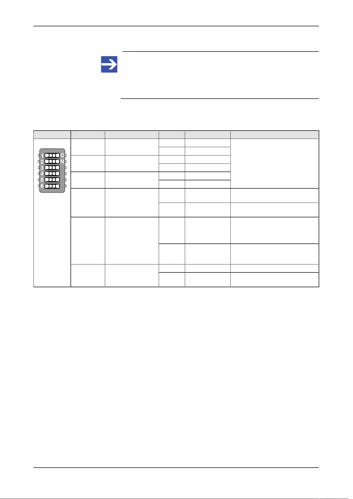
2.3.1 S300 - DIP switches for selecting boot mode and PLL clock speed
For identifying the switches on the board, see position (1) in section
Positions of interfaces and operating elements [}page12].
These switches allow you to:
·select the boot mode
– select the standard boot mode
– enable the console mode
– enable the alternative boot mode
·set the PLL clock speed for the Dual Cortex-A9 to either 400 MHz or
600 MHz
Boot mode
The ROM Code of the netX 4000 features an integrated bootloader that
automatically recognizes the selected boot mode and the initial state of the
device after reset.
The user can select a certain boot sequence option by setting the switches
No 1, No 2 and No 3 of S300 accordingly (see table S300 boot sequence
configuration [}page16]).
Example: If boot sequence option 1 is selected, the ROM resident
bootloader searches for a bootable image in the SQI Flash. If no image is
found, the bootloader continues its search according to the sequence. If the
loader cannot find any image in the sources, it automatically enters the
console mode to enable the initial provisioning of a firmware.
Standard boot mode
In standard boot mode, the ROM resident bootloader searches for a
“standard” bootable firmware image in the boot sources according to the
chosen boot sequence option (see table S300 boot sequence
configuration [}page16]).
Console mode
The purpose of the console mode is to enable the handling of firmware
programming – such as the download of a firmware to the SQI Flash – via a
USB connection (USB socket X301 of the board) from a development PC
(Flasher Tool from Hilscher).
For information about how to use the Flasher Tool from Hilscher for
the NXHX 4000-JTAG+, see Getting Started document NXHX
4000-JTAG+ Development Board, DOC171004GSxxEN.
Note:
Temporarily connecting RDY to ground (S300-E) while carrying out a
reset cycle forces the device into console mode regardless of the
initial state and boot mode settings.
NXHX 4000-JTAG+ | Device description
DOC170703HW02EN | Revision 2 | English | 2018-10 | Released | Public
© Hilscher 2018
Descriptions and drawings 15/70
Alternative boot mode
Note:
The alternative boot mode is not yet supported by the initial version
of the netX 4000.
It will be available on the final version of the netX 4000 in serial
production.
Functions and Settings
The following table shows the functions of the individual switches of S300:
S300 Switch Signal Position Connects to Function
1
(S300-A)
QSPI_SIO2 OFF Internal pull-up Selection of boot sequence option
(see table S300 boot sequence
configuration [}page16])
ON GND via 1.5 kΩ
2
(S300-B)
QSPI_MISO_SIO1 OFF Internal pull-up
ON GND via 1.5 kΩ
3
(S300-C)
QSPI_MOSI_SIO0 OFF Internal pull-up
ON GND via 1.5 kΩ
4
(S300-D)
QSPI_CLK OFF Internal pull-up Sets PLL clock speed for the Dual
Cortex-A9 to 600 MHz
ON GND via 1.5 kΩ Sets PLL clock speed for the Dual
Cortex-A9 to 400 MHz
5
(S300-E)
SYS_RDY# OFF Internal pull-up Device boots according to the
selected boot sequence option (see
table S300 boot sequence
configuration [}page16])
ON GND via 390 Ω Forces the device into console
mode regardless of the boot mode
settings
6
(S300-F)
SYS_RUN# OFF Internal pull-up Disables alternative boot mode
ON GND via 390 Ω Enables alternative boot mode
option (not yet supported)
Table4: Functions of the S300 DIP switches
NXHX 4000-JTAG+ | Device description
DOC170703HW02EN | Revision 2 | English | 2018-10 | Released | Public
© Hilscher 2018

Descriptions and drawings 16/70
The following table shows how to set the S300 switches to select a certain
boot mode:
Boot mode Boot source interface Switch 5
(S300-E)
Switch 6
(S300-F)
S300
switches
Standard boot mode See subsequent table OFF OFF
Console mode USB 1.1 (on-board connector) ON OFF or ON
Alternative boot mode See subsequent table (not yet supported) OFF ON
Table5: S300 boot mode configuration
Note:
If console mode and alternative boot mode option are both
enabled, the console mode always has priority over the
alternative boot mode.
The following table shows how to set the S300 switches to select a certain
boot sequence option. These boot sequence options are valid for both
“standard” and “alternative” boot mode.
Boot
sequence
option
Boot source interfaces / boot sequences Switch 1
(S300-A)
Switch 2
(S300-B)
Switch 3
(S300-C)
S300 switches
1 1. Serial Quad Interface (SQI): 16 MB SQI Flash
2. Secure Digital Input/Output (SDIO): MicroSD Card
3. Real-Time Ethernet Channel 0: DHCP/TFTP server
connection (FAQ in preparation)
ON ON ON
2 1. Serial Quad Interface (SQI): 16 MB SQI Flash
2. Secure Digital Input/Output (SDIO): MicroSD Card
3. Console mode: USB 1.1 Mini-B Device Connector
OFF ON ON
3 1. Serial Quad Interface (SQI): 16 MB SQI Flash
2. Secure Digital Input/Output (SDIO): MicroSD Card
3. Parallel Dual-Port Memory (DPM) via host
interface (HIF): not supported by the board
ON OFF ON
4 1. Serial Quad Interface (SQI): 16 MB SQI Flash
2. Secure Digital Input/Output (SDIO): MicroSD Card
3. Serial Dual-Port Memory (SPM) via host interface
(HIF): NXHX-FTDI USB-to-SPM plug-in module
OFF OFF ON
5Reserved ON ON OFF
6 1. Serial Quad Interface (SQI): 16 MB SQI Flash
2. Secure Digital Input/Output (SDIO): MicroSD Card
3. Real-Time Ethernet LVDS0: not supported by the
board
OFF ON OFF
7 1. Serial Quad Interface (SQI): 16 MB SQI Flash
2. Secure Digital Input/Output (SDIO): MicroSD Card
3. PCIe end point: not supported by the board
ON OFF OFF
8 1. Memory Controller (PL353): no external NOR Flash
memory on the board
2. Serial Quad Interface (SQI): 16 MB SQI Flash
3. Secure Digital Input/Output (SDIO): MicroSD Card
4. Real-Time Ethernet Channel 0: DHCP/TFTP server
connection (FAQ in preparation)
OFF OFF OFF
Table6: S300 boot sequence configuration
NXHX 4000-JTAG+ | Device description
DOC170703HW02EN | Revision 2 | English | 2018-10 | Released | Public
© Hilscher 2018

Descriptions and drawings 17/70
2.3.2 S301 - DIP switches for user-defined inputs
For identifying the switches on the board, see position (4) in section
Positions of interfaces and operating elements [}page12].
S601 Switch Signal Position Connects to
1
(S301-A)
MMIO06_GPIO0_6 OFF -
ON +3.3V via 10 kΩ
2
(S301-B)
MMIO07_GPIO0_7 OFF -
ON +3.3V via 10 kΩ
3
(S301-C)
MMIO08_GPIO0_8 OFF -
ON +3.3V via 10 kΩ
4
(S301-D)
MMIO09_GPIO0_9 OFF -
ON +3.3V via 10 kΩ
Table7: S301 for user-defined inputs
2.3.3 T300 - Power-on reset push button
For identifying the button on the board, see position (12) in section
Positions of interfaces and operating elements [}page12] .
T300 Signal Connects to Function
SENSE_+3V3 GND Resets the full SoC including PLL
and debug settings
Table8: T300 - Power-on-reset button
2.3.4 T301 - Reset push button
For identifying the button on the board, see position (11) in section
Positions of interfaces and operating elements [}page12] .
T301 Signal Connects to Function
JT_RESET_IN# GND Resets the netX
Table9: T301 - Reset button
Important:
The first “engineering sample” version of the netX 4000 has a glitch
concerning the RST_IN# signal (i.e. the JT_RESET_IN# signal of
the T301 reset button on the NXHX 4000-JTAG+ board).
The current workaround is always using the POR# signal (i.e. the
T300 power-on reset button on the board) instead of the RST_IN#
signal for achieving a power cycle.
The POR# signal (i.e. the T300 button) resets the full SoC including
PLL and debug settings, in contrast to the RST_IN# signal (i.e. the
T301 button).
NXHX 4000-JTAG+ | Device description
DOC170703HW02EN | Revision 2 | English | 2018-10 | Released | Public
© Hilscher 2018
Descriptions and drawings 18/70
2.3.5 S1300 – Slide switch for SDRAM/SPM selection at host interface
Slide switch for selecting the host interface mode. For identifying the switch
on the board, see position (17) in section Positions of interfaces and
operating elements [}page12].
Position Connects to Function
Down +3.3V via 10 kΩ Enables the usage of the NXHX-FTDI adapter module
at the X1300 host interface connector, which provides
access to the serial Dual-Port Memory (SPM) interface
from PC or laptop via USB.
Note: If this setting is used, the on-board SDRAM
cannot be used, due to pin sharing restrictions.
Up GND via 10 kΩ The on-board SDRAM can operate in 32-bit data mode.
If this setting is used, the NXHX-FTDI adapter module
cannot be used, due to pin sharing restrictions.
Table10: S1300 switch for SDRAM/SPM selection
NXHX 4000-JTAG+ | Device description
DOC170703HW02EN | Revision 2 | English | 2018-10 | Released | Public
© Hilscher 2018

Descriptions and drawings 19/70
2.4 Interfaces
2.4.1 X300 - JTAG connector
Standard JTAG connector X300 with 20 pins. For identifying the connector
on the board, see position (3) in section Positions of interfaces and
operating elements [}page12].
JTAG connector Pin Signal
1+3V3
2+3V3
3JT_#TRST
4GND
5JT_TDI
6GND
7JT_TMS/SWD+
8GND
9JT_TCLK/SWCLK
10 GND
11 JT_SEL1
12 GND
13 JT_TDO
14 GND
15 JT_#RESET_IN
16 GND
17 Not connected
18 GND
19 JT_+6V9
20 GND
Table11: Pin assignments JTAG connector
2.4.2 X301 - USB 1.1 device connector (“Mini-B” jack)
USB 1.1 device connector (Mini-B) X301 for diagnostics (if supported by
the loadable firmware) and firmware flashing (to external non-volatile
memory). For identifying the connector on the board, see position (13) in
section Positions of interfaces and operating elements [}page12].
USB socket Pin Signal Description
1VBUS Not connected
2D- Data -
3D+ Data +
4 - Not connected
5GND Ground
Shield Connected to GND via 1 MΩ and 10nF
Table12: Pin assignments of Mini-B USB connector
NXHX 4000-JTAG+ | Device description
DOC170703HW02EN | Revision 2 | English | 2018-10 | Released | Public
© Hilscher 2018

Descriptions and drawings 20/70
2.4.3 X800 - USB 2.0 host connector (“Type A” jack)
USB 2.0 host connector (Type A) X800. For identifying the connector on
the board, see position (30) in section Positions of interfaces and operating
elements [}page12].
USB socket Pin Signal Description
1VBUS Output voltage: +5 V DC
Output current: max. 500 mA
2D- Data -
3D+ Data +
4GND Ground
Shield Connected to GND via 1 MΩ and 10nF
Table13: Pin assignments of USB 2.0 host connector
2.4.4 X801 - USB 2.0 device connector (“Type B” jack)
USB 2.0 device connector (Type B) X801. For identifying the connector on
the board, see position (31) in section Positions of interfaces and operating
elements [}page12].
USB Type B jack Pin Signal Description
1VBUS +5V input
2D- Data -
3D+ Data +
4GND Ground
Shield Connected to GND via 1 MΩ and 10nF
Table14: Pin assignments USB 2.0 device connector
2.4.5 X1000/X1100 – Gigabit Ethernet connectors
Two RJ45 jack gigabit Ethernet connectors. For identifying the connectors
on the board, see position (19) for Channel 0 (X1000) and position (18) for
channel 1 (X1100) in section Positions of interfaces and operating
elements [}page12].
Gigabit
Ethernet
Pin Signal Description
1 TX+/D1+ Transmit data positive
Transmit/receive data positive channel 1
2 TX–/D1– Transmit data negative
Transmit/receive data negative channel 1
3 RX+/D2+ Receive data positive
Transmit/receive data positive channel 2
4 D3+ Transmit/receive data positive channel 3
5 D3– Transmit/receive data negative channel 3
6 RX–/D2– Receive data negative
Transmit/receive data negative channel 2
7 D4+ Transmit/receive data positive channel 4
8 D4– Transmit/receive data negative channel 4
Bob Smith termination used
Table15: Gigabit Ethernet RJ45 pin assignment
NXHX 4000-JTAG+ | Device description
DOC170703HW02EN | Revision 2 | English | 2018-10 | Released | Public
© Hilscher 2018
Table of contents
Other hilscher Motherboard manuals

hilscher
hilscher NXHX 51-ETM User manual

hilscher
hilscher NXHX 90-MC Operating and installation instructions

hilscher
hilscher NXHX 51-ETM Operating and installation instructions

hilscher
hilscher NXHX 52-JTAG Operating and installation instructions

hilscher
hilscher NXHX 90-JTAG Operating and installation instructions

hilscher
hilscher NXHX500-RE Quick start guide


