manuals.online logo
Brands
  1. Home
  2. •
  3. Brands
  4. •
  5. Hitachi
  6. •
  7. Microcontroller
  8. •
  9. Hitachi H8S/2633 F-ZTAT User manual

Hitachi H8S/2633 F-ZTAT User manual

This manual suits for next models

6

Popular Microcontroller manuals by other brands

Microsemi IGLOO nano Starter Kit user guide

Microsemi

Microsemi IGLOO nano Starter Kit user guide

GOWIN DK START GW1NSR-LV4CQN48PC7I6 V 1.1 user guide

GOWIN

GOWIN DK START GW1NSR-LV4CQN48PC7I6 V 1.1 user guide

HETRONIC ERGO-S Service manual

HETRONIC

HETRONIC ERGO-S Service manual

Laird BL654PA user guide

Laird

Laird BL654PA user guide

Novatek NT6861 manual

Novatek

Novatek NT6861 manual

Lantronix Intrinsyc Open-Q 865XR SOM user guide

Lantronix

Lantronix Intrinsyc Open-Q 865XR SOM user guide

Nuvoton ISD61S00 ChipCorder Design guide

Nuvoton

Nuvoton ISD61S00 ChipCorder Design guide

STMicrolectronics ST7 Assembler Linker user manual

STMicrolectronics

STMicrolectronics ST7 Assembler Linker user manual

Texas Instruments Chipcon CC2420DK user manual

Texas Instruments

Texas Instruments Chipcon CC2420DK user manual

NEC 78GK0S/K 1+ Series Application note

NEC

NEC 78GK0S/K 1+ Series Application note

Mikroe SEMITECH N-PLC Click Application note

Mikroe

Mikroe SEMITECH N-PLC Click Application note

Intel Agilex user guide

Intel

Intel Agilex user guide

DIGITAL-LOGIC MICROSPACE manual

DIGITAL-LOGIC

DIGITAL-LOGIC MICROSPACE manual

Texas Instruments TMS320F2837 D Series Workshop Guide and Lab Manual

Texas Instruments

Texas Instruments TMS320F2837 D Series Workshop Guide and Lab Manual

CYPRES CY14NVSRAMKIT-001 user guide

CYPRES

CYPRES CY14NVSRAMKIT-001 user guide

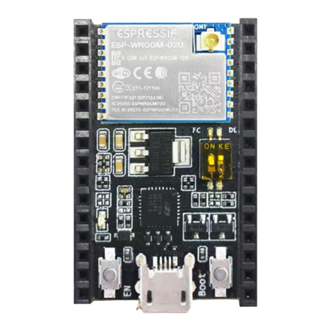
Espressif Systems ESP8266EX Programming guide

Espressif Systems

Espressif Systems ESP8266EX Programming guide

Abov AC33M8128L user manual

Abov

Abov AC33M8128L user manual

Silicon Laboratories C8051F800 user guide

Silicon Laboratories

Silicon Laboratories C8051F800 user guide

manuals.online logo
manuals.online logoBrands
  • About & Mission
  • Contact us
  • Privacy Policy
  • Terms and Conditions

Copyright 2025 Manuals.Online. All Rights Reserved.

H8S/2633 Series
H8S/2633
HD6432633
H8S/2632
HD6432632
H8S/2631
HD6432631
H8S/2633 F-ZTAT™
HD64F2633
Hardware Manual
ADE-602-165A
Rev. 2.0
4/14/00
Hitachi, Ltd.
Cautions
1. Hitachi neither warrants nor grants licenses of any rights of Hitachi’s or any third party’s
patent, copyright, trademark, or other intellectual property rights for information contained in
this document. Hitachi bears no responsibility for problems that may arise with third party’s
rights, including intellectual property rights, in connection with use of the information
contained in this document.
2. Products and product specifications may be subject to change without notice. Confirm that you
have received the latest product standards or specifications before final design, purchase or
use.
3. Hitachi makes every attempt to ensure that its products are of high quality and reliability.
However, contact Hitachi’s sales office before using the product in an application that
demands especially high quality and reliability or where its failure or malfunction may directly
threaten human life or cause risk of bodily injury, such as aerospace, aeronautics, nuclear
power, combustion control, transportation, traffic, safety equipment or medical equipment for
life support.
4. Design your application so that the product is used within the ranges guaranteed by Hitachi
particularly for maximum rating, operating supply voltage range, heat radiation characteristics,
installation conditions and other characteristics. Hitachi bears no responsibility for failure or
damage when used beyond the guaranteed ranges. Even within the guaranteed ranges,
consider normally foreseeable failure rates or failure modes in semiconductor devices and
employ systemic measures such as fail-safes, so that the equipment incorporating Hitachi
product does not cause bodily injury, fire or other consequential damage due to operation of
the Hitachi product.
5. This product is not designed to be radiation resistant.
6. No one is permitted to reproduce or duplicate, in any form, the whole or part of this document
without written approval from Hitachi.
7. Contact Hitachi’s sales office for any questions regarding this document or Hitachi
semiconductor products.
Preface
The H8S/2633 Series is a series of high-performance microcontrollers with a 32-bit H8S/2600
CPU core, and a set of on-chip supporting functions required for system configuration.
The H8S/2600 CPU can execute basic instructions in one state, and is provided with sixteen 16-bit
general registers with a 32-bit internal configuration, and a concise and optimized instruction set.
The CPU can handle a 16 Mbyte linear address space (architecturally 4 Gbytes). Programs based
on the high-level language C can also be run efficiently.
The address space is divided into eight areas. The data bus width and access states can be selected
for each of these areas, and various kinds of memory can be connected fast and easily.
Single-power-supply flash memory (F-ZTAT™*1), PROM (ZTAT™*2), and mask ROM versions
are available, providing a quick and flexible response to conditions from ramp-up through full-
scale volume production, even for applications with frequently changing specifications.
On-chip supporting functions include a 16-bit timer pulse unit (TPU), programmable pulse
generator (PPG), 8-bit timer, 14-bit PWM timer (PWM), watchdog timer (WDT), serial
communication interface (SCI, IrDA), A/D converter, D/A converter, and I/O ports. It is also
possible to incorporate an on-chip PC bus interface (IIC) as an option.
In addition, DMA controller (DMAC) and data transfer controller (DTC) are provided, enabling
high-speed data transfer without CPU intervention.
Use of the H8S/2633 Series enables easy implementation of compact, high-performance systems
capable of processing large volumes of data.
This manual describes the hardware of the H8S/2633 Series. Refer to the H8S/2600 Series and
H8S/2000 Series Programming Manual for a detailed description of the instruction set.
Note: * F-ZTAT (Flexible-ZTAT) is a trademark of Hitachi, Ltd.
Main Revisions and Additions in this Edition
Page Item Revisions
(See Manual for Details)
2 1.1 Overview Table 1-1 Overview
Input clock frequency amended
9 1.3.2 Pin Functions in Each Operating Mode Table 1-2 Pin Functions in Each
Operating Mode amended
14 1.3.3 Pin Functions Table 1-3 Pin Functions amended
38 2.6.1 Overview Table 2-1 Instruction Classification
Notes on TAS Instruction added
39 2.6.2 Instructions and Addressing Modes Table 2-2 Combinations of
Instructions and Addressing Modes
Notes on TAS Instruction added
43, 47 2.6.3 Table of Instructions Classified by Function Table 2-3 Instructions classified by
Function
Notes on TAS Instruction added
66 2.10 Usage Note Added
68 3.2.1 Mode Control Register (MDCR) Bit 7 description amended
75 3.4 Pin Functions in Each Operating Mode Table 3-3 Pin Functions in Each
Mode amended
76 to 78 3.5 Address Map in Each Operating Mode Figure 3-1 Memory Map in Each
Operating Mode in the H8S/2633
Note 2 added
Figure 3-2 Memory Map in Each
Operating Mode in the H8S/2632
Note 2 added
Figure 3-3 Memory Map in Each
Operating Mode in the H8S/2631
Note 2 added, amended
84, 85 4.2.3 Reset Sequence Figure 4-2 Reset Sequence
(Modes 4 and 5) amended
Figure 4-3 Reset Sequence
(Modes 6 and 7) added
87 4.4 Interrupts Figure 4-4 Interrupt Sources and
Number of Interrupts amended
Page Item Revisions
(See Manual for Details)
101 5.3.3 Interrupt Exception Handling Vector Table Table 5-4 Interrupt Sources, Vector
Addresses, and Interrupt Priorities
8-bit timer channel names amended
109 5.4.2 Interrupt Control Mode 0 Figure 5-5 Flowchart of Procedure
Up to Interrupt Acceptance in
Interrupt Control Mode 0 amended
189 7.6.1 DDS=1 Figure 7-30 DACK Output Timing
when DDS=1 (Example Showing
DRAM Access)
Note added
190 7.6.2 DDS=0 Figure 7-31 DACK Output Timing
when DDS=0 (Example Showing
DRAM Access)
Note added
202 7.10.4 Transition Timing Figure 7-39 Bus-Released State
Transition Timing amended
209, 210 8.1.3 Overview of Functions Table 8-1 Overview of DMAC
Functions
SCI transfer source names
amended
290, 291 8.7 Usage Notes DMAC Register Access during
Operation added
Figure 8-40 and figure 8-41 added
296 9.1.2 Block Diagram Figure 9-1 Block Diagram of DTC
amended
310, 311 9.3.3 DTC Vector Table Table 9-4 Interrupt Sources, DTC
Vector Addresses, and
Corresponding DTCEs
8-bit timer channel names amended
327 10.1 Overview Capacitance load value amended
328 to
331 Table 10-1 Port Functions
amended
350 to
352 10.3.3 Pin Functions Table 10-5 Port 3 Pin Functions
amended
363 10.7.1 Overview Figure 10-6 Port A Pin Functions
amended
369 10.8.1 Overview Figure 10-9 Port B Pin Functions
amended
Page Item Revisions
(See Manual for Details)
396 10.12.3 Pin Functions Table 10-21 Port F Pin Functions
PF3 description amended
522 13.1.2 Block Diagram Figure 13-1 Block Diagram of 8-Bit
Timer amended
523 13.1.3 Pin Configuration Table 13-1 Pin Configuration
amended
563 15.1 Overview Amended
566 15.1.4 Register Configuration Table 15-2 WDT Registers
amended
570, 571 15.2.2 Timer Control/Status Register (TCSR) Bits 2 to 0 (overflow period)
amended
573 15.2.4 Pin Function Control Register (PFCR) Amended
587, 588 16.1.4 Register Configuration Table 16-2 SCI Registers
Note 3 amended
597 16.2.6 Serial Control Register (SCR) Description of bits 1 and 0 amended
646 16.3.5 IrDA Operation Figure 16-22 IrDA Transmit and
Receive Operations amended
653 to
658 16.5 Usage Notes Operation in Case of Mode
Transition added
Switching from SCK Pin Function to
Port Pin Function added
18.1.1 Features Formatless description deleted
692, 693 18.1.2 Block Diagram Description amended
Figure 18-1 Block Diagram of I2C
Bus Interface
Dedicated formatless clock deleted
694 18.1.3 Input/Output Pins Table 18-1 I2C Bus Interface Pins
SYNCI pin deleted
699, 700 18.2.2 Slave Address Register (SAR) Bit 0 description amended
701 18.2.3 Second Slave Address Register (SARX) Bit 0 description amended
703 18.2.4 I2C Bus Mode Register (ICMR) Description of bits 5 to 3
ø = 25 MHz added to transfer rates
705, 708,
709 18.2.5 I2C Bus Control Register (ICCR) Bit 7 description added
Bit 1 description amended
Page Item Revisions
(See Manual for Details)
717 18.2.8 DDC Switch Register (DDCSWR) Description of bits 7 to 4 amended
Bits 3 to 0 amended and Note 2
added
Description of CLR3-0 added
719 18.3.1 I2C Bus Data Format Description amended
Figure 18-3 I2C Bus Data Formats
(I2C Bus Formats)
Formatless description deleted
720 to
722 18.3.2 Master Transmit Operation Description amended
722 to
724 18.3.3 Master Receive Operation Description amended
Figure 18-8 Example of Master
Receive Mode Operation Timing
(MLS = WAIT = ACKB = 0)
amended
731, 732 18.3.9 Sample Flowcharts Figure 18-14 Flowchart for Master
Transmit Mode (Example) amended
Figure 18-15 Flowchart for Master
Receive Mode (Example) amended
734 to
736 18.3.10 Initialization of Internal State Added
736, 737,
739, 740 18.4 Usage Notes Table 18-6 I2C Bus Timing (SCL
and SDA Output) amended
Table 18-7 Permissible SCL Rise
Time (tSr) Values ø = 25 MHz added
to time indication
Table 18-8 I2C Bus Timing (with
Maximum Influence of tSr/tSf)
amended
740 to
743 Note on ICDR Read at End of
Master Reception added
Notes on Start Condition Issuance
for Retransmission added
Notes on I2C Bus Interface Stop
Condition Instruction Issuance
added
745 19.1.1 Features Conversion time amended
753 19.2.3 A/D Control Register (ADCR) Bit 3 and 2 (conversion time)
amended
Page Item Revisions
(See Manual for Details)
760 19.4.3 Input Sampling and A/D Conversion Time Conversion time amended
761 Table 19-4 A/D Conversion Time
(Single Mode) amended
766 19.6 Usage Notes Permissible Signal Source
Impedance amended
771 20.1.4 Register Configuration Table 20-2 D/A Converter
Registers amended
778 21.2.1 System Control Register (SYSCR) Description of bit 0
Note added
779 21.4 Usage Notes Reserved Areas amended
781 22.1 Features Programming/Erasing amended
792, 793 22.5.2 Flash Memory Control Register 2
(FLMCR2) Amended
797, 798 22.5.7 Serial Control Register X (SCRX) Amended
801 22.6.1 Boot Mode Automatic SCI Bit Rate Adjustment
Bit rate amended
803, 804 22.6.2 User Program Mode Description amended
805 to
812 22.7 Programming/Erasing Flash Memory Completely revised
821 22.11.1 Socket Adapter Pin Correspondence
Diagram Figure 22-17 Socket Adapter Pin
Correspondence Diagram amended
822 22.11.2 Programmer Mode Operation Table 22-11 Settings for Various
Operating Modes In Programmer
Mode amended
834 to
838 22.13 Flash Memory Programming and Erasing
Precautions Added
839 22.14 Note on Switching from F-ZTAT Version to
Mask ROM Version Added
842 23.2.1 System Clock Control Register (SCKCR) Description amended
843, 844 23.2.2 Low-Power Control Register (LPWRCR) Amended
844 23.3 Oscillator Amended
Page Item Revisions
(See Manual for Details)
844, 845 23.3.1 Connecting a Crystal Resonator Table 23-2 Damping Resistance
Value
25 MHz added
Crystal Resonator amended
845, 846 Table 23-3 Crystal Resonator
Parameters
25 MHz added
Figure 23-5 Points for Attention
when Using PLL Oscillation Circuit
amended
848 23.3.2 External Clock Input External Clock
Description amended
Table 23-4 External Clock Input
Conditions amended
849 23.4 PLL Circuit Amended
854 24.1 Overview Table 24-1 LSI Internal States in
Each Mode
WDT module stop mode description
amended
860, 861 24.2.2 System Clock Control Register (SCKCR) Description amended
871 24.6.3 Setting Oscillation Stabilization Time after
Clearing Software Standby Mode Table 24-5 Oscillation Stabilization
Time Settings
25 MHz added
25.2 Power supply voltage and operating
frequency range Deleted
Following item numbers amended
880 to
887 25.2 DC Characteristics Amended
888 25.3 AC Characteristics Figure 25-1 Output Load Circuit
amended
889 25.3.1 Clock Timing Table 25-5 Clock Timing amended
893, 894,
901 25.3.3 Bus Timing Table 25-7 Bus Timing amended
Figure 25-15 External Bus Request
Output Timing added
902 25.3.4 DMAC Timing Table 25-8 DMAC Timing amended
Page Item Revisions
(See Manual for Details)
906 to
908 25.3.5 Timing of On-Chip Supporting Modules Table 25-9 Timing of On-Chip
Supporting Modules
Note added
Figure 25-21 PPG Output Timing
amended
914 25.4 A/D Conversion Characteristics Table 25-11 A/D Conversion
Characteristics
Conditions amended
915 25.5 D/A Conversion Characteristics Table 25-12 D/A Conversion
Characteristics
Conditions amended
916 25.6 Flash Memory Characteristics Added
925, 927,
942 A.1 Instruction List Table A-1 Instruction Set
Notes on TAS Instruction added
MULXU and MULXS instruction
execution states amended
956, 957 A.2 Instruction Codes Table A-2 Instruction Codes
Notes on TAS Instruction added
974, 975 A.4 Number of States Required for Instruction
Execution Table A-5 Number of Cycles in
Instruction Execution
Notes on TAS Instruction added
988, 989 A.5 Bus States During Instruction Execution Table A-6 Instruction Execution
Cycles
Notes on TAS Instruction added
996 to
1005 B.1 Addresses Completely revised
1006 to
1103 B.2 Functions Completely revised