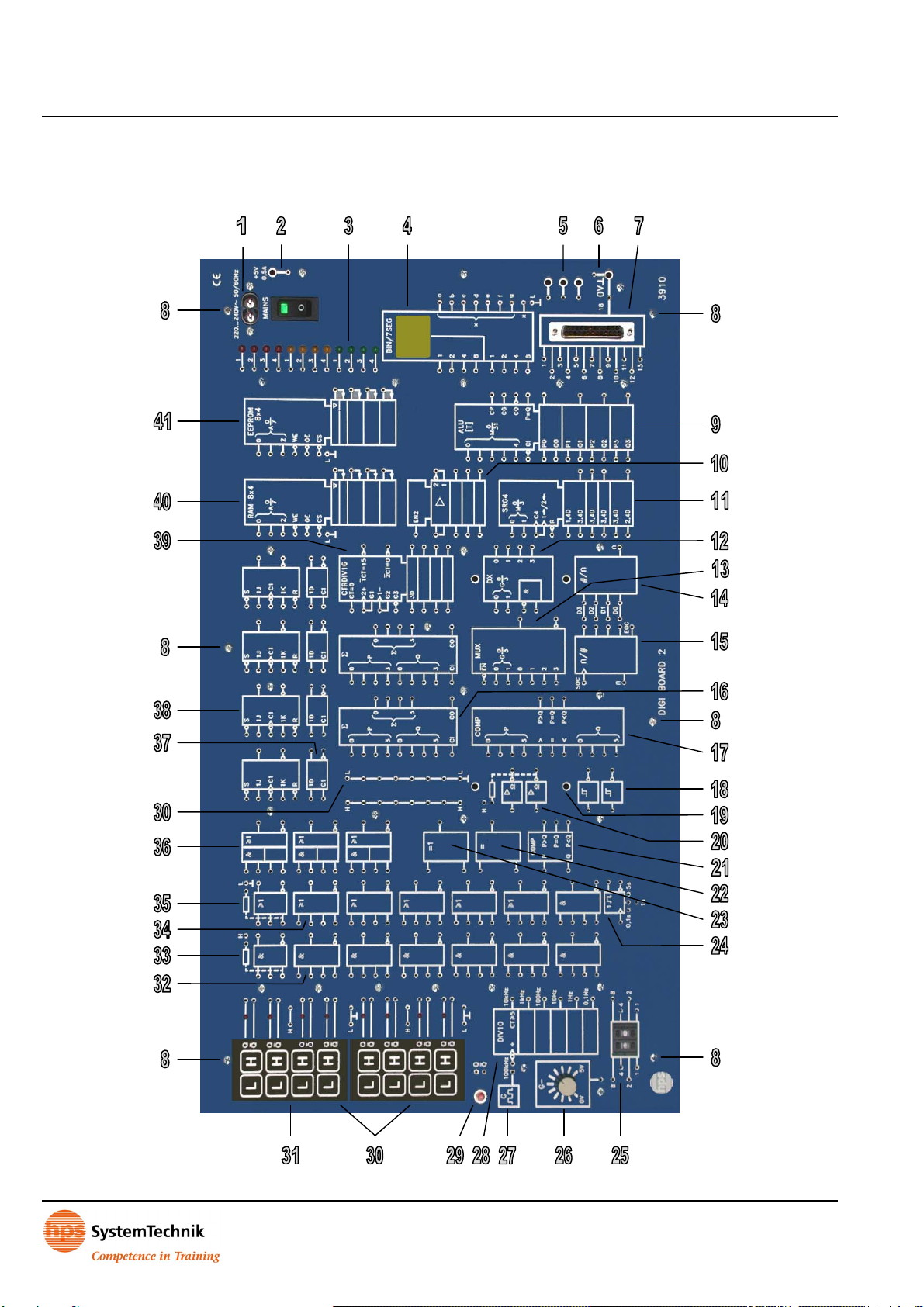
8DIGI BOARD 2
Typ(e) 3910
GBD
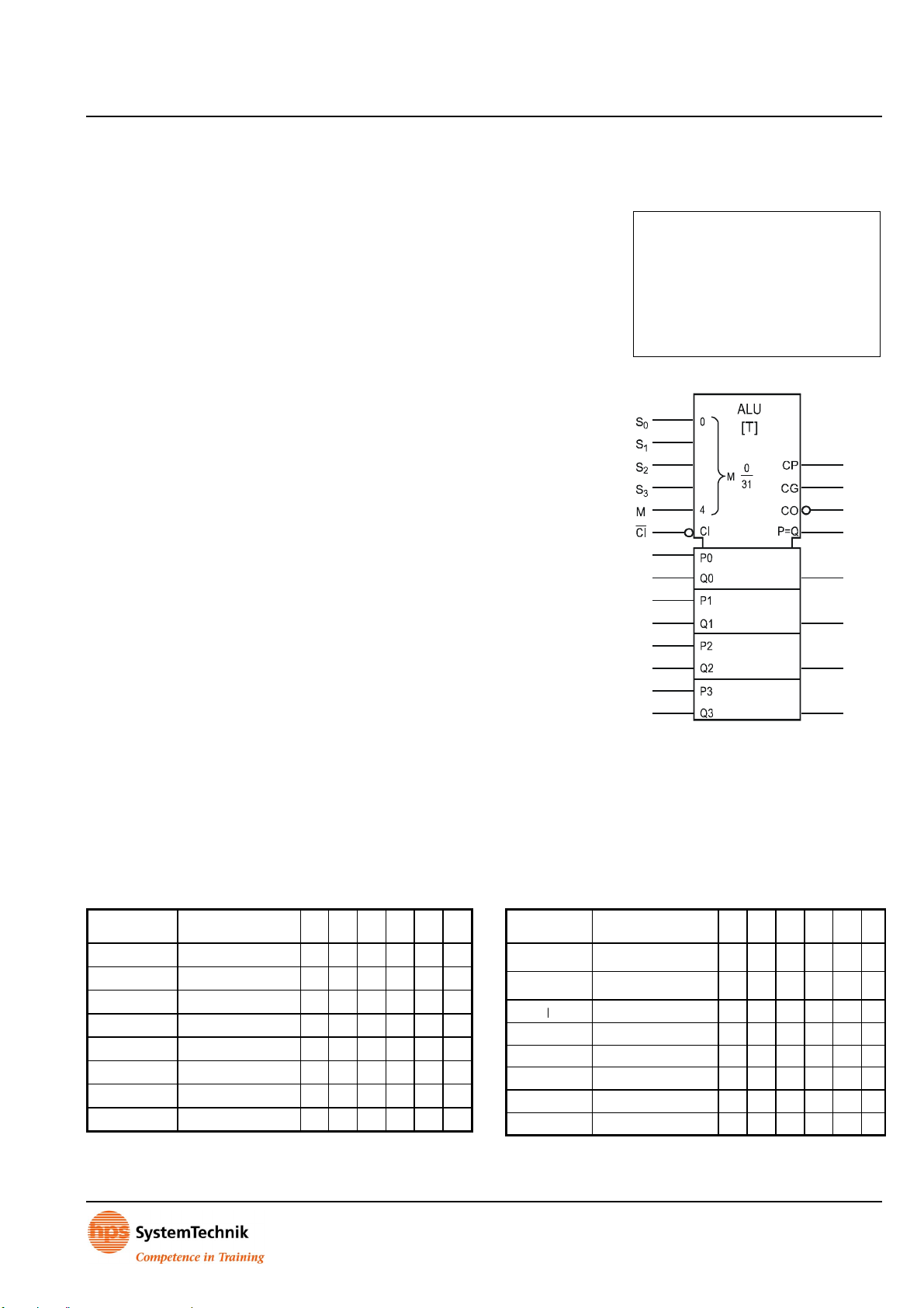
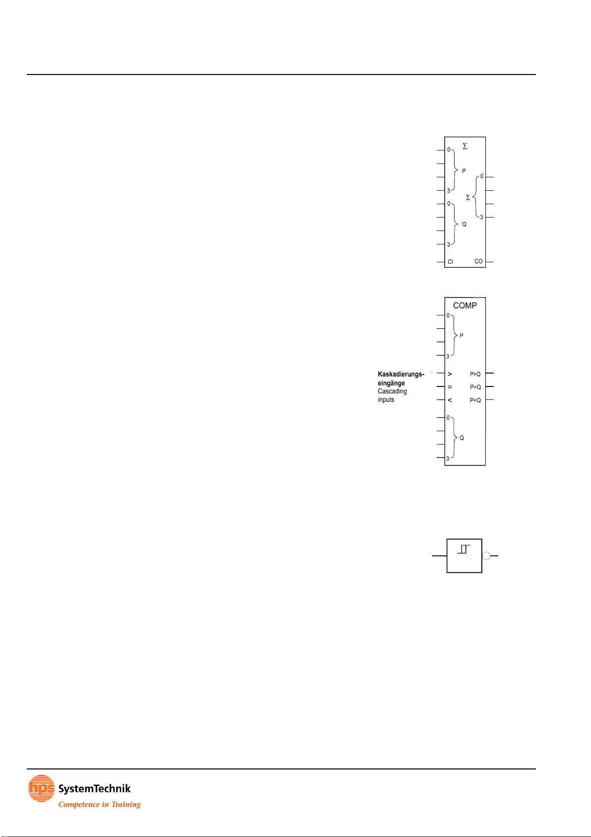
(16) Addierer
Zwei Volladdierer (4 Bit) mit Über-
tragseingang (CI = Carry in) und
Übertragsausgang (CO = Carry out)
zur Addition von zwei 4-Bit-Dual-
zahlen (siehe Abb. 11). Wird das
Ergebnis > F, so muss am Über-
tragsausgang der Zustand von Low
auf High wechseln. Wird an den
Übertragseingang ein High-Pegel
gelegt, so erhöht sich das Ergebnis
um „1“.
(17) 4-Bit-Komparator
Komparator zum Vergleich von
zwei 4-Bit-Dualzahlen (Abb. 12) mit
Kaskadierungseingängen (>, =, <).
Die Kaskadierungseingänge sind
im Gegensatz zu den P- und Q-Ein-
gängen nicht mit Pull-up-Widerstän-
den beschaltet. Es besteht zusätz-
lich die Möglichkeit, zwei 5-Bit-Dual-
zahlen miteinander zu vergleichen,
indem die Ausgänge des 1-Bit-
Komparators (siehe Punkt 21) auf
die Kaskadierungseingänge des
4-Bit-Komparators aufgeschaltet
werden. Die Eingänge des 1-Bit-
Komparators werden dabei zusätz-
lich benutzt.
(18) Schmitt-Trigger
Zwei invertierende Schmitt-Trigger,
keine Pull-up-/Pull-down-Beschal-
tung, auch als Inverter einsetzbar
(Abb. 13). Werden die Schmitt-
Trigger z.B. am Eingang mit der
Gleichspannungs-Signalquelle (sie-
he Punkt 26) beschaltet, kann die
Schalthysterese aufgezeigt werden.
(19) Modul-Steckfeld
Zwei Steckfelder mit je zwei 4-mm-
Buchsen (Steckerabstand: 57 mm)
zur Aufnahme von zusätzlichen
steckbaren Modulen (Serie 9400)
• Versorgungsspannung: 5 V DC /
max. 1 A (kurzschlussfest)
(16) Adder
Two full adders (4 bits) with carry in
(CI) and carry out (CO) for addition of
two 4-bit dual numbers (see fig. 11).
If the result becomes > F, the state
must change from low to high at the
carry output. If a high level is applied
to the carry input, the result is incre-
mented by „1“.
(17) 4-Bit Comparator
Comparator for comparing two 4-bit
dual numbers (fig. 12) with cascad-
ing inputs (>, =, <). The cascading
inputs are not wired with pull-up re-
sistors in opposition to the P and Q
inputs. It is also possible to compare
two 5-bit dual numbers by connect-
ing the outputs of the 1-bit compara-
tor (see item 21) to the cascading
inputs of the 4-bit comparator. The
inputs of the 1-bit comparator are
then used additionally.
(18) Schmitt Trigger
Two inverting Schmitt triggers, no
pull-up/pull-down wiring, can also
be used as inverters (fig. 13). The
switching hysteresis can be shown
for example if the Schmitt triggers
are connected to the DC voltage
signal source (see item 26) on the
input side.
(19) Module Connector Field
Two connector fields with two 4-mm
acks each (plug spacing: 57 mm)
for plugging in additional modules
(series 9400)
• Voltage supply: 5 V DC / max. 1 A
(short-circuit-proof)
Abb. 11 – Fig. 11
Abb. 12 – Fig. 12
Abb. 13 – Fig. 13