Icom IC-M700PRO Building instructions

S-14410XZ-C1
June. 2007
SSB RADIO TELEPHONE
iC-m700pro

This service manual describes the latest service information
for the IC-M700PRO SSB RADIO TELEPHON at the time of
publication.
NEVER connect the transceiver to an AC outlet or to a DC
power supply that uses more than specified. This will ruin
the transceiver.
DO NOT expose the transceiver to rain, snow or any liquids.
DO NOT reverse the polarities of the power supply when
connecting the transceiver.
DO NOT apply an RF signal of more than 20 dBm (100 mW) to
the antenna connector. This could damage the transceiver’s
front-end.
To upgrade quality, any electrical or mechanical parts and
internal circuits are subject to change without notice or
obligation.
MODEL VERSION ALARM UNIT
IC-M700PRO
GEN-1 N/A
GEN-2 Yes
GEN-21 N/A
GEN-22 Yes
GEN-24 N/A
GEN-25 Yes
CHN N/A
Be sure to include the following four points when ordering
replacement parts:
1. 10-digit Icom parts numbers
2. Component name
3. Equipment model name and unit name
4. Quantity required
<ORDER EXAMPLE>
1110003491 S.IC TA31136FNG IC-M700PRO MAIN UNIT 5 pieces
8820001210 Screw 2438 screw IC-M700PRO Top cover 10 pieces
Addresses are provided on the inside back cover for your
convenience.
Icom, Icom Inc. and logo are registered trademarks of Icom Incorporated (Japan) in the United States, the United
Kingdom, Germany, France, Spain, Russia and/or other countries.
ORDERING PARTS
1. Make sure the problem is internal before disassembling
the transceiver.
2. DO NOT open the transceiver until the transceiver is
disconnected from its power source.
3. DO NOT force any of the variable components. Turn
them slowly and smoothly.
4. DO NOT short any circuits or electronic parts. An
insulated tuning tool MUST be used for all adjustments.
5. DO NOT keep power ON for a long time when the
transceiver is defective.
6. DO NOT transmit power into a Standard Signal
Generator or a Sweep Generator.
7. ALWAYS connect a 50 dB to 60 dB attenuator between
the transceiver and a Deviation Meter or Spectrum
Analyzer when using such test equipment.
8. READ the instructions of test equipment throughly
before connecting a test equipment to the transceiver.
REPAIR NOTES
INTRODUCTION CAUTION

CONTENTS
SECTION 1 SPECIFICATIONS
SECTION 2 INSIDE VIEWS
SECTION 3 CIRCUIT DESCRIPTION
3 - 1 RECEIVER CIRCUITS ................................................................................................................................ 3 - 1
3 - 2 TRANSMITTER CIRCUITS ......................................................................................................................... 3 - 3
3 - 3 PLL CIRCUIT............................................................................................................................................... 3 - 5
3 - 4 PORT ALLOCATIONS ................................................................................................................................. 3 - 6
SECTION 4 ADJUSTMENT PROCEDURES
4 - 1 PREPARATION ............................................................................................................................................ 4 - 1
4 - 2 PLL ADJUSTMENT ..................................................................................................................................... 4 - 2
4 - 3 TRANSMITTER ADJUSTMENTS................................................................................................................ 4 - 4
4 - 4 RECEIVER ADJUSTMENTS....................................................................................................................... 4 - 8
SECTION 5 PARTS LIST
SECTION 6 MECHANICAL PARTS AND DISASSEMBLY
SECTION 7 SEMICONDUCTOR INFORMATION
SECTION 8 BOARD LAYOUTS
8 - 1 PLL UNIT .................................................................................................................................................... 8 - 1
8 - 2 MAIN UNIT ................................................................................................................................................. 8 - 2
8 - 3 LOGIC-J UNIT, ALARM AND PA150W BOARD'S ...................................................................................... 8 - 3
8 - 4 MIC-J, VR1/2-J, SENSOR1/2, FILTER-J AND TERMINAL-J BOARD'S...................................................... 8 - 4
SECTION 9 BLOCK DIAGRAM
SECTION 10 VOLTAGE DIAGRAM
LOGIC-J UNIT, VR1/2-J, SENSOR1/2-J AND MIC-J BOARD'S .............................................................. 10 - 1
MAIN UNIT ................................................................................................................................................ 10 - 2
PLL UNIT .................................................................................................................................................. 10 - 5
PA150W, FILTER-J, TERMINAL-J BOARD'S .......................................................................................... 10 - 6

1 - 1
SECTION 1 SPECIFICATIONS
MGENERAL
• Frequency coverage : Receive 500 kHz–29.9999 MHz
Transmit 1.6000–2.9999 MHz 4.0000–4.9999 MHz
6.0000–6.9999 MHz 8.0000–8.9999 MHz
12.0000–13.9999 MHz 16.0000–17.9999 MHz
18.0000–19.9999 MHz 22.0000–22.9999 MHz
25.0000–27.50000 MHz
• Mode : J3E (USB), H3E (AM), J2B (AFSK), F1B (FSK), R3E, A1A (CW)
(Available modes differ with version)
• Number of channels : 150 channels (max.)—3 groups of 50 channels each
• Antenna impedance : 50 Ω (nominal)
• Usable temperature range : –30˚C to +60˚C; –22˚F to +140˚F
• Frequency stability : ±10 Hz (–30˚C to +60˚C; –22˚F to +140˚F)
(±20 Hz above 15 MHz)
• Power supply requirement : 13.6 V DC ±15% Negative ground
• Current drain (at 13.6 V DC) : Transmit (max. output power) 30 A
Receive (max. audio output) 2.5 A
• Dimensions (projections not included) : 291.4(W)×116.4(H)×315(D) mm; 1115⁄32(W)×419⁄32(H)×1213⁄32(D) in
• Weight (with ant., battery case and cells) : 7.9 kg; 17 lb 7 oz
• Remote connector : NMEA D-sub 9-pin (female)
• ACC 1 connector : DIN 8-pin (female)
• ACC 2 connector : DIN 7-pin (female)
MTRANSMITTER
• Output power (at 13.6 V DC) : 150, 60, 20 W PEP
(60, 20 W PEP only above 24 MHz)
• Spurious emissions : –75 dB typical
• Carrier suppressions : 65 dB typical
• Unwanted sideband suppression : 75 dB typical
• Microphone impedance : 600 Ω
MRECEIVER
• Sensitivity :
J3E, R3E, J2B, A1A 0.35 µV typical (1.8000–29.9999 MHz)
(for 12dB SINAD) 1.0 µV (1.6000–1.7999 MHz)
6.3 µV (0.5000–1.5999 MHz)
H3E (for 10dB S/N) 2.2 µV typical (1.8000–29.9999 MHz)
6.3 µV (1.6000–1.7999 MHz)
32 µV (0.5000–1.5999 MHz)
• Spurious response rejection : 80 dB (1.6000–29.9999 MHz)
• Audio output power : 5.0 W typical (at 10% distortion with a 4 Ωload)
• Audio impeadance : 4 to 8 Ω
• Clarity variable range : ±150 Hz
All stated specifications are subject to change without notice or obligation.

2 - 1
SECTION 2 INSIDE VIEWS
• PA150W, FILTER AND TERMINAL BOARDS
TERMINAL board
Fuse
(F7001)
Drive amplifiers
(Q4001, Q4002: 2SC3133)
Thermal switches
S4001: OHD-3 110M
S4002: OHD-3 50M
Power amplifiers
(Q4003, Q4004: 2SC2904)
PA150W board
REG board
[EUR-21], [EUR-22] onl
y
FILTER board
Power detector circuit
• MAIN, PLL AND LOGIC UNITS
RF filter circuit
Noise blanker circuit
2nd mixer circuit
1st IF amplifier
(Q8: 3SK131)
1st IF filter
(FI1: FL-120)
PLL IC
(IC3005: LC7153M)
DDS IC
(IC3001: SC-1246A)
PLL/-A unit
ALARM board
except [GEN-21]
MAIN unit
Squelch circuit
Demodulator circuit
(IC10: NJM1496V)
BFO DDS IC
(IC3002: SC-1287)
Reference oscillator
(X3001: CR-282)
[GEN-21], [GEN-22],
[EUR-21] only
LOGIC unit

3 - 1
SECTION 3 CIRCUIT DESCRIPTION
3-1 RECEIVER CIRCUITS
3-1-1 RF FILTER CIRCUIT (MAIN UNIT)
Received signals from the antenna connector pass through
the transmit/receive switching relay (FILTER board RL4317)
and are then applied to the MAIN unit via J2.
The signals pass through the protection relay (RL2),
1.6 MHz cut off high-pass filter (L2–L4, C4–C8, C629) and
are then applied to one of nine bandpass filters (including
one low-pass filter for below 2.0 MHz). These filters are
selected by the filter control signals (B0–B8) as described
in the table below.
The filtered signals pass through the 30 MHz cut-off low-
pass filter (L71, L72, C130–C134, C618), and are then
applied to the 1st mixer circuit (Q6, Q7).
• RF FILTERS USED
3-1-2 1ST MIXER AND IF CIRCUITS (MAIN UNIT)
The 1st mixer circuit converts the received signals into a
fixed frequency, 69.0115 MHz 1st IF signal using the PLL
output frequency. By changing the PLL frequency, only the
desired frequency is picked up at the pair of crystal filters
(FI1a, FI1b) at the next stage.
The IF amplifier (Q8) and resonator circuits are designed
between the filter pair. The PLL output signal (1LO) enters
the MAIN unit via J3 and is amplified at the 1st LO ampli-
fier (Q5) and then applied to the 1st mixer (Q6, Q7)
3-1-3 2ND MIXER AND IF CIRCUITS (MAIN UNIT)
The 1st IF signal from the crystal filter (FI1b) is converted
again into a 9.0115 MHz 2nd IF signal at the 2nd mixer
circuit (D52, L66, L67). The 60 MHz 2nd local signal (2LO)
from the PLL unit enters the MAIN unit via J4 to be applied
to the 2nd mixer.
The 2nd IF signal is passed through the noise blanker gate
(D15, D16) and amplified at the 2nd IF amplifier (Q16) and
then applied to one of the 9 MHz IF filters as described
below. The passed signal is amplified at the two stage 2nd
IF amplifiers (Q32, Q33) and is applied to a demodulator
circuit (D39 for H3E or IC10 for J3E and others).
• 2ND IF FILTERS USED
3-1-4 NOISE BLANKER CIRCUIT (MAIN UNIT)
The noise blanker circuit cuts off the IF circuit line at the
moment of receiving a pulse-type noise.
A portion of the 2nd IF signal between resonator circuits
(L83, L84 after stage of the 2nd mixer, D52) is amplified
at the noise amplifiers (Q9, IC8, Q11). The signal is then
detected at the noise detector (D17) to convert the noise
components to DC voltages.
The signals are then applied to the noise blanker switch
(Q13, Q14). At the moment the detected voltage exceeds
the Q13’s threshold level, Q14 outputs a blanking signal
to close the noise blanker gate (D15, D16) by applying
reverse-biased voltage. Q15 turns the noise blanker circuit
ON and OFF.
LPF or
BPF
0.5–29.999 MHz
1st mixer
Q6, Q7
1st LO:
69.5115–99.0115 MHz
Fl1a/Fl1b
Crystal
filter
Crystal
filter
69.0115 MHz
2nd mixer
D52
2nd LO: 60.0 MHz
Fl2 or
Fl3/Fl4
9.0115 MHz Other modes
H3E Detector
D39
Demodulator
IC10
Audio output
BFO
J3E, J2B, R3E, FSK:
FSK narrow, J2B narrow:
A1A:
9.013 MHz
9.0123 MHz
9.0116 MHz
Frequency
(MHz)
0.5–1.999
2–2.999
3–4.999
5–6.999
7–9.999
Frequency
(MHz)
10–13.999
14–17.999
18–23.999
24–29.999
Control
signal
B5
B6
B7
B8
Control
signal
B0
B1
B2
B3
B4
Entrance
coil
L49
L8
L13
L18
L23
Entrance
coil
L28
L33
L38
L43
MODE
J3E, R3E, FSK
H3E
FSK narrow,
A1A narrow
Used filter
FI2
FI3/FI4
Optional narrow
filter*
Control signal
SEL8: low, H3E8: low
SEL8: low, H3E8: high
SEL8: high, H3E8: low
• RECEIVE FREQUENCY CONSTRUCTION
*Built-in to the GMDSS versions

3 - 2
The detected voltage is also applied to the noise blanker
AGC circuit (Q12, Q10) and is then fed back to the noise
amplifier (IC8) as a bias voltage. The noise AGC circuit
prevents closure of the noise blanker gate for long periods
by non-pulse-type noise. The time constant of the noise
blanker AGC circuit is determined by R58 and C114.
3-1-5 DEMODULATOR CIRCUIT (MAN UNIT)
This circuit mixes the 2nd IF and BFO signals to pick up
the AF components (except H3E mode). The 2nd IF signal
from the 2nd IF amplifier (Q33) is applied to the balanced
mixer (IC10, pin 1). The 9.0116–9.0130 MHz BFO signal
from the PLL unit is also applied to IC10 (pin 10). AF sig-
nals are output from pin 12 and are then applied to the AF
circuits.
3-1-6 H3E DETECTOR CIRCUIT (MAIN UNIT)
The 2nd IF signal from the 2nd IF amplifier (Q33) is applied
to the AM detector circuit (D39) to be demodulated into AF
signals. The detected signals are amplified at the buffer
amplifier (Q45), and are then applied to the AF circuits.
3-1-7 AGC CIRCUIT (MAIN UNIT)
The AGC (Automatic Gain Control) circuit reduces IF ampli-
fier gain to prevent the receiver circuit from distorting and
to keep the audio output at a constant level.
A portion of the IF signals from the 2nd IF amplifier (Q33)
is detected at the AGC detector circuit (D31) and is then
applied to the AGC amplifier (Q41) to control the AGC time
constant line. The reference voltage of the AGC line is con-
trolled by the “RFG” line which comes from the CPU for the
RF gain setting.
When receiving a strong signal, the detected voltage
increases and the voltage of the AGC line is decreased by
the AGC amplifier (Q41) via the –5 V voltage line. The AGC
line is used for the bias voltage of the IF amplifiers (Q8,
Q16, Q32, Q33), so that these amplifiers reduce gain.
When the strong signal disappears, the AGC line voltage is
released by C245/R268 and C670/R813.
The AGC switch (Q42, D38) turns the AGC circuit OFF
when the AGC OFF function activates. The AGC-fast switch
(Q131) sets the AGC line as fast-release during scanning,
A1A mode selection and DSC operation.
3-1-8 S-METER CIRCUIT (MAIN UNIT)
The S-meter indicates the AGC level on the display, since
the AGC level varies with the received signal strength.
The AGC bias voltage (AGC time constant line) from the
AGC amplifier (Q41) is inverted and amplified at the meter
amplifier (IC19b). The amplified signal is applied to the
CPU via the “RSM” line.
3-1-9 AF AMPLIFIER CIRCUITS
(MAIN UNIT AND LOGIC BOARD)
AF signals from the demodulator or H3E detector circuits
pass through the active low-pass filter (IC20b) and squelch
gate (IC12a), and are then applied to the electronic volume
control (IC36). The CPU (IC132, pin 37) outputs the volume
control signal (1 to 5 V) according to the [VOLUME] control
setting.
The AF output signal from IC36 (9 pin) are supplied to
the LOGIC unit via J23. The signals are amplified at the
AF power amplifier (IC2007) and are then applied to the
internal speaker via microphone connector (pins 3, 4) and
external [SP] jack via the MAIN unit.
The speaker switch relay (RL2001) is connected to the (–)
terminal of internal speaker for the [SPEAKER] switch func-
tion.
3-1-10 SQUELCH CIRCUIT (MAIN UNIT)
The transceiver has two squelch circuits, voice activated
squelch for J3E/H3E and S-meter squelch for A1A/F1B/
J2B.
(1) AF ACTIVATED SQUELCH
A portion of the AF signal from the active low-pass filter
(IC20b) is amplified at the limiter amplifier (IC20a) and is
then applied to the one-shot multi-vibrator (IC22c, IC22d).
The one shot multi-vibrator functions as an F-V converter
which generates a signal only when audio signals are
received.
The output signals pass through the NOR gate (IC22b) and
then the 3 Hz low-pass filter (IC21a) to remove the remain-
ing noise components. The filtered signal is applied to the
window comparator (IC21b). The NOR gate (IC22b) deac-
tivates the audio activated squelch during A1A/F1B/J2B
mode operation.
1st IF signal
Q8 D52 Q16
2nd IF filters
Q32 Q33
H3E derector
Demodulator
8 V
CW, DSC,
SCAN
Q131 C670
R813
C245
C268
AGC time
constant line
RFG (RF gain control)
0 to 5 V
– 5 V Q41 Q42
D31 AGC detector
AGC OFF control
AGC amplifier
AGC-fast control
• AGC CIRCUIT

3 - 3
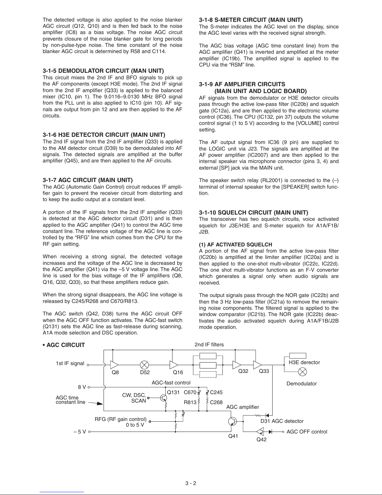
The comparator outputs “High” when the integrated signals
exceed the reference voltage. C269, R310 and R780 are
used as a time constant circuit. The resulting signal output
from IC22a is inverted at Q46 and is then applied to the
CPU as the “SQLS” signal. The CPU controls the squelch
gate (IC12a) when the “SQLS” signal is received.
(2) S-METER SQUELCH
The S-meter signal from IC19b is applied to the squelch
comparator (IC19a) to close or open the squelch circuit.
The reference voltage is adjusted by R257 and then
applied to the (–) terminal of the comparator (IC19a). When
the S-meter signal exceeds the reference voltage, the com-
parator outputs “High” to the CPU via IC22a and Q46 in the
same manner as the voice activated squelch circuit.
3-2 TRANSMITTER CIRCUITS
3-2-1 MICROPHONE AMPLIFIER CIRCUIT
(LOGIC BOARD)
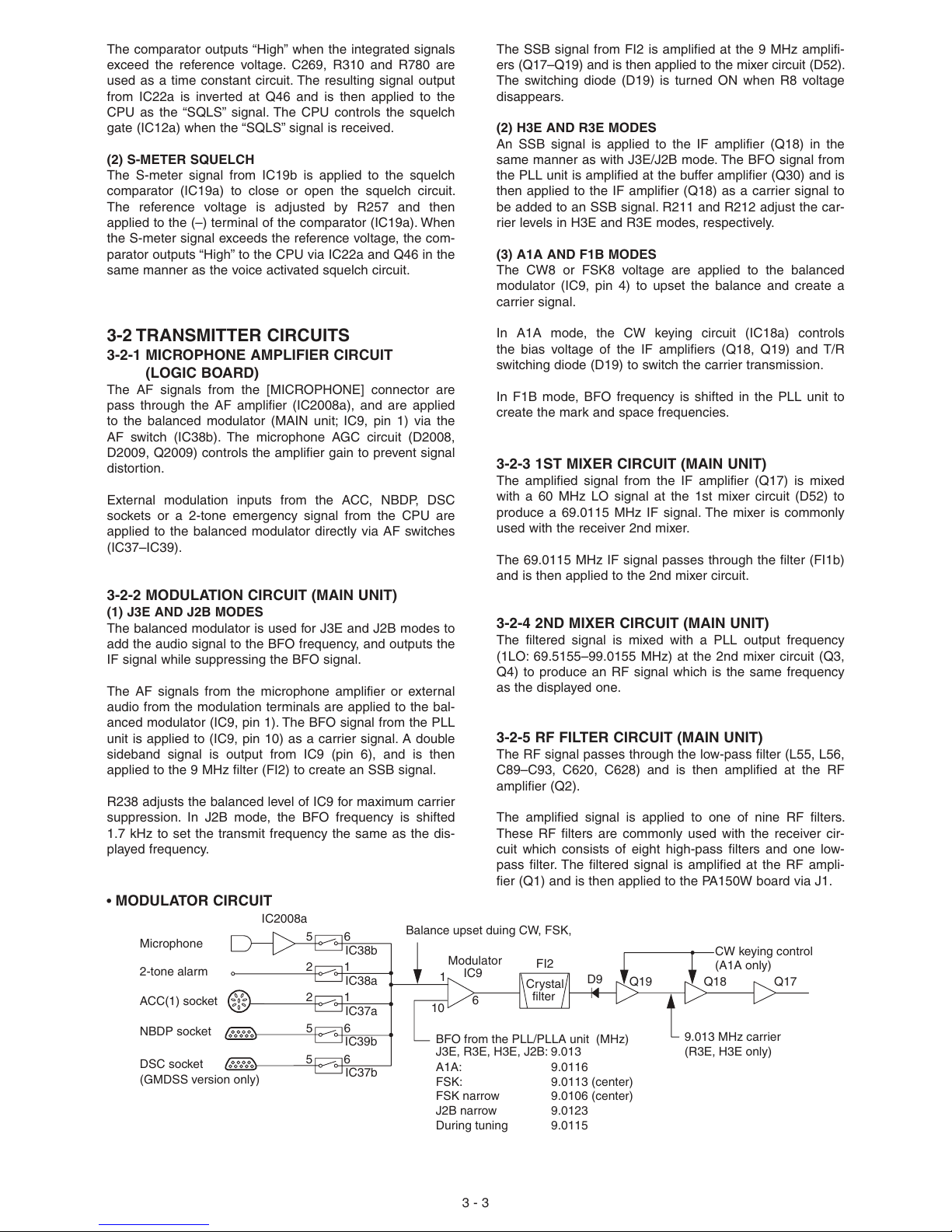
The AF signals from the [MICROPHONE] connector are
pass through the AF amplifier (IC2008a), and are applied
to the balanced modulator (MAIN unit; IC9, pin 1) via the
AF switch (IC38b). The microphone AGC circuit (D2008,
D2009, Q2009) controls the amplifier gain to prevent signal
distortion.
External modulation inputs from the ACC, NBDP, DSC
sockets or a 2-tone emergency signal from the CPU are
applied to the balanced modulator directly via AF switches
(IC37–IC39).
3-2-2 MODULATION CIRCUIT (MAIN UNIT)
(1) J3E AND J2B MODES
The balanced modulator is used for J3E and J2B modes to
add the audio signal to the BFO frequency, and outputs the
IF signal while suppressing the BFO signal.
The AF signals from the microphone amplifier or external
audio from the modulation terminals are applied to the bal-
anced modulator (IC9, pin 1). The BFO signal from the PLL
unit is applied to (IC9, pin 10) as a carrier signal. A double
sideband signal is output from IC9 (pin 6), and is then
applied to the 9 MHz filter (FI2) to create an SSB signal.
R238 adjusts the balanced level of IC9 for maximum carrier
suppression. In J2B mode, the BFO frequency is shifted
1.7 kHz to set the transmit frequency the same as the dis-
played frequency.
The SSB signal from FI2 is amplified at the 9 MHz amplifi-
ers (Q17–Q19) and is then applied to the mixer circuit (D52).
The switching diode (D19) is turned ON when R8 voltage
disappears.
(2) H3E AND R3E MODES
An SSB signal is applied to the IF amplifier (Q18) in the
same manner as with J3E/J2B mode. The BFO signal from
the PLL unit is amplified at the buffer amplifier (Q30) and is
then applied to the IF amplifier (Q18) as a carrier signal to
be added to an SSB signal. R211 and R212 adjust the car-
rier levels in H3E and R3E modes, respectively.
(3) A1A AND F1B MODES
The CW8 or FSK8 voltage are applied to the balanced
modulator (IC9, pin 4) to upset the balance and create a
carrier signal.
In A1A mode, the CW keying circuit (IC18a) controls
the bias voltage of the IF amplifiers (Q18, Q19) and T/R
switching diode (D19) to switch the carrier transmission.
In F1B mode, BFO frequency is shifted in the PLL unit to
create the mark and space frequencies.
3-2-3 1ST MIXER CIRCUIT (MAIN UNIT)
The amplified signal from the IF amplifier (Q17) is mixed
with a 60 MHz LO signal at the 1st mixer circuit (D52) to
produce a 69.0115 MHz IF signal. The mixer is commonly
used with the receiver 2nd mixer.
The 69.0115 MHz IF signal passes through the filter (FI1b)
and is then applied to the 2nd mixer circuit.
3-2-4 2ND MIXER CIRCUIT (MAIN UNIT)
The filtered signal is mixed with a PLL output frequency
(1LO: 69.5155–99.0155 MHz) at the 2nd mixer circuit (Q3,
Q4) to produce an RF signal which is the same frequency
as the displayed one.
3-2-5 RF FILTER CIRCUIT (MAIN UNIT)
The RF signal passes through the low-pass filter (L55, L56,
C89–C93, C620, C628) and is then amplified at the RF
amplifier (Q2).
The amplified signal is applied to one of nine RF filters.
These RF filters are commonly used with the receiver cir-
cuit which consists of eight high-pass filters and one low-
pass filter. The filtered signal is amplified at the RF ampli-
fier (Q1) and is then applied to the PA150W board via J1.
2-tone alarm
ACC(1) socket
NBDP socket
DSC socket
(GMDSS version only)
IC2008a
5
2
2
5
5
6
6
6
1
1
IC38b
IC38a
IC37a
IC39b
IC37b
Balance upset duing CW, FSK,
Modulator
IC9
1
10 6
FI2
BFO from the PLL/PLLA unit (MHz)
J3E, R3E, H3E, J2B: 9.013
A1A:
FSK:
FSK narrow
J2B narrow
During tuning
9.0116
9.0113 (center)
9.0106 (center)
9.0123
9.0115
Crystal
filter
D9 Q19 Q18
CW keying control
(A1A only)
Q17
9.013 MHz carrier
(R3E, H3E only)
Microphone
•MODULATOR CIRCUIT

3 - 4
3-2-6 POWER AMPLIFIER CIRCUIT
(PA150W BOARD)
This circuit provides a stable 150 W (at 13.6 V) of output
power. The RF signal from the MAIN unit is amplified at the
pre-driver (Q4008), drivers (Q4001, Q4002), and power
amplifiers (Q4003, Q4004).
The driver and power amplifiers form class AB push-pull
circuits. Bias voltage to these transistors is produced by
diodes (D4001–D4003) which have temperature junctions
with the transistors.
The amplified signal is then applied to one of eight low-
pass filters to suppress high harmonic components. The
filtered signal passes through the power detector circuit
(FILTER board; L4341) and transmit/receive switching relay
(FILTER board; RL4317) and is then applied to the antenna
connector.
• LOW-PASS FILTERS USED (FILTER BOARD)
3-2-7 ALC CIRCUIT
The transceiver has two ALC (Auto Level Control) loops for
constant output power over all marine bands and for high
power setting.
(1) IF ALC CIRCUIT (MAIN UNIT)
A portion of the IF signals from the IF amplifier (Q17) is
applied to the IF ALC circuit. The signal is amplified at
Q126 and then detected at the ALC detector (D46). The
detected signal is amplified at the ALC amplifier (IC17b)
and is then applied to the comparator (IC17a).
The reference voltage for the comparator is set by R184.
The antenna tuning control voltage (TUN8) and low power
set signal (POC1) are also affected by the reference volt-
age to decrease the IF signal level.
The comparator output controls the gate bias of the IF
amplifier (Q19), so that the IF signal level is determined by
the reference voltage of the comparator (IC17a).
(2) RF ALC CIRCUIT (FILTER BOARD)
The RF output power level is detected at D4309 of the
power detector circuit (FILTER board; L4341, D4309,
D4310). The detected signal (“FOR” signal) is applied to
the RF ALC amplifier (MAIN unit; IC16a).
The amplified signal enters the transmit gain controller
(IC16b) which functions as an inversion amplifier. The gain
controller decrease the gain of the IF amplifier (MAIN unit;
Q2) to constant output power from differential amplifier
gains which are occurred by their frequency characteristics.
The bias voltage of the RF ALC amplifier (IC16a) is con-
trolled by the low power control signal (POC1 for 20 W,
POC2 for 60 W) and APC signal.
Q19 Q18 Q17
IF ALC CIRCUIT
IC17a IC17b
Q126
20 W low power set (Q132)
Current APC
– 5 V
High power set (R184)
Low power during tune (Q28)
D52 Q3, Q4 Q2 Q1
8 V
Current APC control (Q111)
Low power during tune (Q21, Q22)
RF ALC CIRCUIT
Q4008
Q4001
Q4002 Q4003
Q4004 L4313
IC16b IC16a Q23
60 W power set (Q24)
20 W power set (Q25)
D4309
FOR
REF
D4310
MAIN UNIT PA UNIT FILTER UNIT
Frequency
(MHz)
0.5–1.999
2–2.999
3–4.999
5–6.999
7–9.999
Frequency
(MHz)
10–13.999
14–17.999
18–19.999
20–21.999
22–23.999
24–29.999
Control
signal
L5
L6
L7
Control
signal
L0
L1
L2
L3
L4
Entrance
Relay
RL4301
RL4303
RL4305
RL4307
RL4309
Entrance
Relay
RL4311
RL4313
RL4315
• ALC CIRCUIT

3 - 5
3-2-8 APC CIRCUIT
The APC (Auto Power Control) circuit protects the power
amplifiers on the PA unit from high SWR and excessive
current.
(1) SWR APC (FILTER BOARD AND MAIN UNIT)
The reflected wave signal appears and increases on the
antenna connector. When the antenna is mismatched,
D4310 of the power detector circuit (FILTER board; D4309,
D4310, L4341) detects the signal and applies it to the APC
amplifier (MAIN unit; Q23). The amplified signal decreases
the bias voltage of the RF ALC amplifier to reduce the out-
put power.
(2) CURRENT APC (PA150W BOARD AND MAIN UNIT)
The power transistor current is detected from the differ-
ent voltages between both terminals of a 0.012 Ω resistor
(R4026) on the PA150W board. The detected voltage is
applied to the differential amplifier (IC4002b). When the cur-
rent of the final transistors is more than 30 A, the detected
voltage is applied to the APC amplifier controller (MAIN
unit; Q111) to reduce the gate-2 voltage of the IF amplifier
(MAIN unit; Q2) and thus reduce the output power.
3-2-9 TEMPERATURE DETECTION
(PA150W BOARD)
Thermal switches (S4001, S4002) protect the final transis-
tors from excessive temperatures. When the temperature of
the final transistors exceeds 50˚C (122˚F), S4002 is turned
ON to start the cooling fan. When the temperature of the
final transistors exceeds 110˚C (230˚F), S4001 is turned
ON to control the “POC2” line and sets the power to 60 W.
3-2-10 RF METER CIRCUIT (MAIN UNIT)
The output of the ALC amplifier (IC16a) is applied to the
CPU (pin 31) to indicate the transmit power level on the
display.
For antenna current meter indication, the “ANTC” signal
from an optional AT-130E is applied to the CPU (pin 32).
3-3 PLL CIRCUIT
3-3-1 GENERAL
The PLL unit generates a 1st LO frequency (69.5115–
99.0114 MHz), 2nd LO frequency (60 MHz) and a BFO fre-
quency (9.0106–9.013 MHz) for the MAIN unit. The 1st LO
PLL adopts a mixerless dual loop PLL system. The BFO
uses a DDS and a 2nd LO as a fixed frequency double that
the crystal oscillator.
3-3-2 1ST LO PLL (PLL UNIT)
The 1st LO PLL contains a main loop and reference loop
as a dual loop system. The reference loop generates a
10.65 to 10.75 MHz frequency using a DDS circuit, and the
main loop generates a 69.5115 to 99.0114 MHz frequency
using the reference loop frequency.
(1) REFERENCE LOOP PLL
The oscillated signal at the reference VCO (Q3005, D3003)
is amplified at the buffer amplifiers (Q3006, Q3011) and is
then applied to the DDS IC (IC3001, pin 46). The signal is
then divided and detected on phase with the DDS gener-
ated frequency.
The detected signal output from IC3001 (pin 56) is convert-
ed into a DC voltage (lock voltage) at the loop filter (R3018,
R3019, C3044) and then fed back to the varactor diode
(D3003) in the VCO circuit.
(2) MAIN LOOP PLL
The oscillated signal at the main loop VCO (Q3003, D3004)
is amplified at the buffer amplifiers (Q3004, Q3008), and is
then applied to the PLL IC (IC3005, pin 14). The signal is
then divided and detected on phase with the reference loop
output frequency.
The detected signal output from IC3005 (pins 3009, 3010)
is converted into a DC voltage (lock voltage) at the loop
filter and then fed back to the varactor diode (D3004) in the
VCO circuit.
The oscillated signal is amplified at the buffer amplifiers
(Q3004, Q3021, Q3024) and then applied to the MAIN unit
as a 1st LO signal.
PLL IC (IC3005)
Programmable
divider
Programmable
divider
Programmable
divider
Programmable
divider
Phase
Phase
detector
detector
DDS
D/A
convertor
convertor
Loop filter
Loop filter
Q3011
Reference loop VCO
Q3005/D3003
Q3008
Main loop VCO
Q3004
Q3003/D3004
10.65–10.75 MHz
Q3006
DDS
IC3002
Q3002
Doubler
D/A
Reference OSC
(
X3001; 30.0 MHz
)
Q3021 Q3024
1LO
(69.5115–99.0114 MHz)
2LO
(60.0 MHz)
BFO
(9.0106–9.013 MHz)
DDS IC
(IC3001)
• PLL CIRCUIT

3 - 6
3-3-3 2ND LO AND REFERENCE OSCILLATOR
CIRCUITS
The reference oscillator (X3001) generates 30.0 MHz fre-
quency used for the both DDS ICs as a system clock and
for the LO output. The oscillated signal is doubled at the
driver (Q3002) and picked up the 60 MHz frequency at
the resonator circuit (L3004, L3005). The 60 MHz signal is
applied to the MAIN unit as a 2nd LO signal.
3-3-4 BFO CIRCUIT
The DDS IC (IC3002) generates a 10-bit digital signal
using the 30 MHz system clock. The digital signal is con-
verted to an analog wave signal at the D/A converter (R3120
–R3139). The analog wave is passed through the low-pass
filter (L3037, L3038, C3154–C3158), and is then applied
to the MAIN unit as the BFO signal. The PA unit separate
grounding from the other units to obtain floating.
1
10
11
16
17
18
20
21
22
23
24
25
26
27
28
30
31
32
33
34
35
36
Input port for the CPU reset signal.
When receiving a “LOW” pulse, the
CPU is reset.
Data input port from the sub CPU in
the FRONT unit.
Data output port to the sub CPU in
the FRONT unit.
Input port to the sub CPU in the
FRONT unit.
Outputs low power control signal for
60 W power.
Outputs low power control signal for
20 W power.
Input port for the CW keying.
High: When key is closed.
Outputs a “SEND” control signal for
the ACC (1) and ACC (2) sockets.
Outputs a “SEND” control signal for
T8 and R8 voltage line control.
Low : For transmit.
Outputs an alarm control signal to
activate the 2-tone emergency alarm
encoder.
High : Alarm ON.
Outputs a tone switching signal for the
2-tone emergency alarm encoder.
High : High tone.
Outputs a clock signal for the
EEPROM (IC134).
Data bus line for the EEPROM
(IC134).
Outputs a serial signal for the
EEPROM (IC135).
Data bus line for the EEPROM
(IC135).
Input port for the S-meter indication.
Input port for the RF-meter indication.
Input port for the antenna current
meter indication for [EUR] version.
The ANTC signal can be received
when an optional AT-130E is con-
nected.
Input port for the squelch detected
signal.
High : When squelch is open.
Input port for the transmit/receive
switching signal.
Input port for the scan control signal
from the ACC (1) socket.
Outputs RF gain control signal to the
AGC circuit.
3-4 PORT ALLOCATIONS
CPU (MAIN unit; IC132)
RES
RXDO
TXDO
NSEN
POC2
POC1
CWIN
ASEN
CSEN
ALMS
ALMC
SCL
SDA
SO
SDA
RSM
MFOR
ANTC
SQLS
TRC
SCAS
RFG
Pin Port Description
number name

3 - 7
37
39
40
41
42
48
49
50
51
52
53
54
55
57–60
61–64
65–67
68
69
70
71
72
Outputs AF gain control signal to the
control (IC36).
Outputs the "tuner start" pulse to an
optional AT-130E.
Outputs a BEEP signal (1 kHz or
500 Hz).
Outputs a strobe signal to the main
loop PLL IC (C3005).
Outputs a strobe signal to the refer-
ence loop DSS IC (IC3001).
Outputs a strobe signal to the BFO
PLL IC (IC3002).
Outputs a data signal to PLL and
DDS ICs.
Outputs a clock signal to PLL and
DDS ICs.
Outputs an AF mute signal for squelch
function.
High : Squelch closed.
Outputs a “noise blanker” signal.
High : Noise blanker is on
Outputs an AGC -OFF signal.
High: AGC deactivate.
Outputs an external NBDP equip-
ment control signal.
Low: During NBDP data output.
Outputs a strobe signal for an initial
matrix.
Input ports for an initial matrix.
Output band signals for RF LPF and
BPF selection.
Outputs mode signals.
Input port for an optional AT-130E.
Low : During tuning.
Outputs a mode signal.
Outputs an antenna tuner tuning
control signal for transceiver’s power/
mode control.
Outputs a narrow filter selection sig-
nal.
Low : Optional narrow filter selec-
tion.
Outputs a program scan control signal
for “AGC fast” and “audio squelch”
deactivation.
AFG
STAT
BEEP
STB1
STB2
STB3
DATA
CK
SQL C
NBS
AGCS
NMS
P20
P17–P14
PD–PA
J2B, R3E,
H3E
KEY
CW
TUNE
FSEL
PROG
(MAIN unit; IC132)–Continued
Pin Port Description
number name

4 - 1
SECTION 4 ADJUSTMENT PROCEDURE
4-1 PREPARATION
• REQUIRED TEST EQUIPMENT
• CONNECTION
EQUIPMENT
DC power supply
RF power meter
(terminated type)
Frequency counter
RF voltmeter
DC voltmeter
Spectram analyzer
GRADE AND RANGE
Output voltage : 13.6 V DC
Current capacity : 30 A or more
Measuring range : 10–200 W
Frequency range : 1.8–30 MHz
Impedance : 50 Ω
SWR : Less than 1.2 : 1
Frequency range : 0.1–100 MHz
Frequency accuracy : ±1 ppm or better
Sensitivity : 100 mV or better
Frequency range : 0.1–100 MHz
Measuring range : 0.01–10 V
Input impedance : 50 Ω/V DC or better
Frequency minimum : At least 90 MHz
Spectraum bandwidth : 100 kHz or more
EQUIPMENT
Audio generator
Standard signal
generator (SSG)
Oscilloscope
AC millivoltmeter
External speaker
Attenuator
DC ammeter
GRADE AND RANGE
Frequency range : 300–3000 Hz
Measuring range : 1–500 mV
Frequency range : 0.1–30 MHz
Output level : 0.1 µV–32 mV
(–127 to –17 dBm)
Frequency range : DC–100 MHz
Measuring range : 0.01–10 V
Measuring range : 10 mV–10 V
Input impedance : 4 Ω
Capacity : 6 W or more
Power attenuation : 50 or 60 dB
Capacity : 150 W or more
Measurement capability: 1 A/3 A/50 A
Spectrum
analyzer
Attenuator
50 or 60 dB
DC power supply
13.6 V/30 A
to DC power receptacle
to [MICROPHONE]
IC-M700PRO
[ANT]
to [EXT SP]
[DC 13.6 V]
Audio
generator
Connect pins 3 and 4
for AF output
Pin 7 MICE
[PTT]
6
54
3
Pin 1 MIC
Speaker
• [MICROPHONE] connector (front view)
AC
millivoltmeter
RF power meter
200 W/50 Ω
Standard signal
generator
CAUTION:
DO NOT connect the
signal generator while
transmitting.

4 - 2
4-2 PLL ADJUSTMENTS
REFERENCE
LOOP LOCK
VOLTAGE
MAIN LOOP
LOCK
VOLTAGE
REFERENCE
FREQUENCY
ADJUSTMENT
ADJUSTMENT ADJUSTMENT CONDITION MEASUREMENT VALUE
POINT
UNIT LOCATION UNIT ADJUST
1
2
1
2
1
2
• Display frequency : 7.9999 MHz
• Mode : J3E
• Receiving
• Display frequency : 0.0300 MHz
• Display frequency : 0.5000 MHz
• Receiving
• Display frequency : 29.9999 MHz
• Wait for 5 min. after power ON.
• Terminate P3002 to ground with a
50 ohms resister.
• Receiving
PLL
PLL
PLL
Connect a digital
multimeter or
oscilloscope to check
point J3004.
Connect a digital
multimeter or
oscilloscope to check
point J3005.
Connect an RF
voltmeter to check
point P3002.
Connect a frequency
counter to check
point P3002.
3.2 V
More than 1.5 V
4.0 V
More than 1.0 V
Maximum level
(More than +2 dBm)
60.000000 MHz
PLL
PLL
PLL
C3049
Verify
L3024
Verify
L3004,
L3005
L3003

4 - 3
Main loop
lock voltage
adjustment
L3024
Main loop
lock voltage
check point
J3005
Reference loop
lock voltage
check point
J3004
Reference loop
lock voltage
adjustment
C3049
Reference
frequency
check point
P3002
Reference
frequency
adjustment
L3004
L3003
L3005
• MAIN AND PLL UNITS

4 - 4
4-3 TRANSMITTER ADJUSTMENTS
IDLING
CURRENT
(For drive
transistors)
(For final
transistors)
IC APC
SWR
DETECTOR
TRANSMIT
PEAK
ADJUSTMENT
ADJUSTMENT ADJUSTMENT CONDITION MEASUREMENT VALUE
POINT
UNIT LOCATION UNIT ADJUST
1
2
1
1
2
1
• Display frequency : 12.2300 MHz
• mode : J3E
• Apply no audio signal to the
[MICROPHONE] connector.
• Transmitting
• Display frequency : 12.2300 MHz
• mode : J3E
• Apply no audio signal to the
[MICROPHONE] connector.
• Transmitting
• Display frequency : 22.0000 MHz
• Mode : J3E
• Preset R4031 on the PA unit to
the maximum counterclockwise
position.
• Connect a dummy load (10 A)
between lead of R4035 (power
line) and EP4009 (power ground)
on the PA unit.
• Connect an audio generator to the
[MICROPHONE] connector and set
as:
Frequency : 1.5 kHz
Level : 100 mV rms
• Connect an RF power meter to the
[ANT] connector.
• Transmitting
• Display frequency : 22.0000 MHz
• Mode : J3E
• Ground the lead of R545 on the
MAIN unit with a wire.
• Connect an audio generator to the
[MICROPHONE] connector and set
as:
Frequency : 1.5 kHz
• Transmitting
• Display frequency : 12.2300 MHz
• Mode : J3E
• Ground the lead of R545 on the
MAIN unit with a wire.
• Connect an audio generator to the
[MICROPHONE] connector and set
as:
Frequency : 1.5 kHz
Level : 3 mV
• Transmitting
PA
PA
Rear
Panel
Rear
Panel
MAIN
Rear
Panel
Cut the lead wire
(W4011) and connect
a DC ammeter (1 A)
to the cut points.
Unsolder R4026
and connect the DC
ammeter (3 A) to the
unsoldered points.
Connect a DC
ammeter (50 A)
between the DC
power supply and
DC power receptacle
(DC input +).
Connect an RF
power meter to the
[ANT] connector.
Connect a DC
voltmeter to R150.
Connect an RF
power meter to the
[ANT] connector.
100 mA
500 mA
30 A
140 W
Minimum level
Maximum output power
PA
PA
PA
Audio
generator
FILTER
MAIN
R4022
R4025
R4031
Output
level
C4392
Adjust in
sequence
L89, L88,
L65, L64,
L59
After adjustment, re-solder the lead wire (W4011).
After adjustment, re-solder R4026.
After adjustment, remove the dummy load.
After adjustment, remove the wire from R545.

4 - 5
SWR detector
adjustment
IC APC
preparation
IC APC check point
Ammeter
1
45
23
789
DC power
supply
EP4009
R4035
10 A dummy
load
C4392
Idling current
(for final transistors)
adjustment
R4025
IC APC adjustment
R4031
Idling current
(for final transistors)
check point
Ammeter
R4026
EP4006
EP4004
Ammeter
EP4003
Unsolder
Cut
W4011
R4026
Idling current
(for drive transistors)
check point
W4011
Idling current
(for drive transistors)
adjustment
R4022
• PA AND FILTER BOARDS
Transmit peak
adjustment
SWR detector
check point
R150
L59
L64
L88
L89
L65
SWR detector
transmit peak
preparation
R545
• MAIN UNIT

4 - 6
TRANSMITTER ADJUSTMENTS (continued)
TRANSMIT
GAIN
OUTPUT
POWER
CARRIER
SUPPRESSION
TUNE
POWER
POWER
METER
MIC
LIMITTER
MIC GAIN
ADJUSTMENT
ADJUSTMENT ADJUSTMENT CONDITION MEASUREMENT VALUE
POINT
UNIT LOCATION UNIT ADJUST
1
2
1
2
3
1
1
1
2
1
1
• Display frequency : 12.2300 MHz
• mode : A1A
• Transmitting
• Display frequency : 16.3650 MHz
• Transmitting
• Display frequency : 12.2300 MHz
• Mode : H3E
• Apply no audio signal to the
[MICROPHONE] connector.
• Transmitting
• Mode : R3E
• Transmitting
• Mode : A1A
• Transmitting
• Display frequency : 12.2300 MHz
• Mode : J3E
• Apply no audio signal to the
[MICROPHONE] connector.
• Transmitting
• Display frequency : 12.2300 MHz
• Ground the lead of L108 (KEY
line) on the MAIN unit with a wire.
• Transmitting
• While pushing the [SQL] and [ENT]
switches, turn power ON.
• Display frequency : 12.2300 MHz
• Mode : J3E
• Connect an audio generator to the
[MICROPHONE] connector and
set as:
Frequency : 1.5 kHz
Level : 100 mV
• Set the transmit power:
[PO-1] (20 W
PEP)
• Transmitting
• Display frequency : 12.2300 MHz
• Mode : J3E
• Disconnect BFO plug (J5) on the
MAIN unit.
• Connect an audio generator to the
[MICROPHONE] connector and
set as:
Frequency : 1.5 kHz
Level : 150 mV
• Transmitting
• Display frequency : 12.2300 MHz
• Mode : J3E
• Connect an audio generator to the
[MICROPHONE] connector and
set as:
Frequency : 1.5 kHz
Level : 10 mV
• Transmitting
140 W
0.5 V
45 W
2.0 W
140 W
Minimum carrier level
(Less than –40 dB)
10 W
17 W
Push the [DIMMER]
switch.
70 mV PEP
100 W
Rear
Panel
MAIN
Rear
Panel
Rear
Panel
Rear
Panel
Rear
Panel
MAIN
Rear
Panel
Connect an RF
power meter to the
[ANT] connector.
Connect a digital
multimeter to R159.
Connect an RF
power meter to the
[ANT] connector.
Connect a spectrum
analyzer or RF
voltmeter to the [ANT]
connector via an
attenuator.
Connect an RF
power meter to the
[ANT] connector.
Connect an RF
power meter to the
[ANT] connector.
Connect an
oscilloscope to R243.
Connect an RF
power meter to the
[ANT] connector.
MAIN
MAIN
MAIN
MAIN
Audio
generator
Font
Panel
LOGIC
LOGIC
R184
R26
R211
R212
R184
Adjust
alternately
R238,
R239
R205
Output
level
[DIMMER]
R2070
R2066

4 - 7
Transmit gain
check point
Transmit
gain
adjustment
R159
R26
R184
Tune power
preparation
Tune power
adjustment
Output power
adjustment
L108
R205
Mic gain
adjustment
R2066
R184
R211
R212
Mic limitter
adjustment
R2070
Carrier
suppression
adjustment
R239
R238
• MAIN UNIT AND LOGIC BOARD

4 - 8
4-4 RECEIVER ADJUSTMENTS
RECEIVER
GAIN
CLARITY
TOTAL GAIN
S-METER
NOISE
BLANKER
ADJUSTMENT
ADJUSTMENT ADJUSTMENT CONDITION MEASUREMENT VALUE
POINT
UNIT LOCATION UNIT ADJUST
1
1
1
2
1
2
1
• Display frequency : 2.1820 MHz
• Mode : J3E
• Noise blanker : OFF
• Squelch : OFF
• Speaker : OFF
• AGC : ON
• RF gain : 9
• R223 (MAIN unit) :
Max. clockwise
• R257 (MAIN unit) : Max.counter
clockwise
• R300 (MAIN unit) : Center
• Connect a standard signal
generator to the [ANT] connector
and set as:
Frequency : 2.1815 MHz
Level : 0.5 µV
(–113 dBm)
modulation : OFF
• Receiving
• While pushing the [SQL] and [CL]
switches, turn power ON.
• Display frequency : 12.2300 MHz
• Mode : J3E
• Connect a standard signal
generator to the [ANT] connector
and set as:
Frequency : 12.2315 MHz
Level : 0.32 mV
(–57 dBm)
modulation : OFF
• Receiving
• Set the signal generator to OFF (no
output).
• While pushing the [SQL] and [T
ONLY] switchs, turn power ON.
• Display frequency : 12.2300 MHz
• Mode : J3E
• Connect a standard signal
generator to the [ANT] connector
and set as:
Frequency : 12.2315 MHz
Level : 1 mV
(–47 dBm)
• Receiving
• Display frequency : 12.2300 MHz
• Mode : J3E
• Connect a standard signal
generator to the [ANT] connector
and set as:
Frequency : 12.2315 MHz
Level : 3.2 µV
(–97 dBm)
Add the following signal into
the signal generator output.
• Receiving
Muximum output level
1.0 V
–30 dB (32 mV)
Push the [DIMMER]
switch.
7th dot just appears
while pushing the
[DIMMER].
Adjust the maximum
noise wave displayed
on the oscilloscope.
Adjust in
sequence
L74, L75,
L78, L79,
L83, L84,
L85, L92,
L93
[CLARITY]
[VOLUME]
R223
[DIMMER]
Verify
L80, L81
Connect an AC
millivoltmeter to the
[EXT SP] jack with a
4 dummy load.
Connect an AC
millivoltmeter to the
[EXT SP] jack with a
4 ohms dummy load.
S/RF meter
Connect an
oscilloscope to R59.
MAIN
Front
Panel
Front
Panel
MAIN
Font
Panel
MAIN
Rear
Panel
Rear
Panel
Function
display
MAIN
Set the [CLARITY] control to the center position and
push the [DIMMER] switch.
12 3 4
1 msec.
100 msec.
This output level of the standard signal generator (SSG) is indicated as SSG’s open circuit.
Other manuals for IC-M700PRO
4
Table of contents
Other Icom Telephone manuals
Popular Telephone manuals by other brands

Grandstream Networks
Grandstream Networks GXP2130 Series user guide

Siemens
Siemens hicom 150 H optiset E standard operating instructions

AT&T
AT&T DEFINITY 8101 user guide

Avaya
Avaya IP Office TransTalk MDW 9040 Quick reference guide

Aastra
Aastra IntelliGate A150 user guide

Mitel
Mitel 6737 Quick reference guide