Icom IC-M710RT User manual

SERVICE
MANUAL
MF/HF MARINE TRANSCEIVER
iM710RT
IC-M710RT-00 99.6.23 11:10 AM Page 1

INTRODUCTION
This service manual describes the latest service information
for the IC-M710RT MF/HF MARINE TRANSCEIVER at the
time of publication.
To upgrade quality, any electrical or mechanical parts and
internal circuits are subject to change without notice or
obligation.
DANGER
NEVER connect the transceiver to an AC outlet or to a DC
power supply that uses more than 16 V. This will ruin the
transceiver.
DO NOT expose the transceiver to rain, snow or any liquids.
DO NOT reverse the polarities of the power supply when
connecting the transceiver.
DO NOT apply an RF signal of more than 20 dBm (100 mW)
to the antenna connector. This could damage the trans-
ceiver’s front end.
ORDERING PARTS
Be sure to include the following four points when ordering
replacement parts:
1. 10-digit order numbers
2. Component part number and name
3. Equipment model name and unit name
4. Quantity required
<SAMPLE ORDER>
1160000130 IC TD62783AF
IC-M710RT
MAIN UNIT 05 pieces
8810009400 Screw
PH M3x8 SUS ZK IC-M710RT
Rear panel 10 pieces
Addresses are provided on the inside back cover for your
convenience.
REPAIR NOTES
1. Make sure a problem is internal before disassembling the
transceiver.
2. DO NOT open the transceiver until the transceiver is dis-
connected from its power source.
3. DO NOT force any of the variable components. Turn
them slowly and smoothly.
4. DO NOT short any circuits or electronic parts. An insu-
lated tuning tool MUST be used for all adjustments.
5. DO NOT keep power ON for a long time when the trans-
ceiver is defective.
6. DO NOT transmit power into a signal generator or a
sweep generator.
7. ALWAYS connect a 50 dB to 60 dB attenuator between
the transceiver and a deviation meter or spectrum ana-
lyzer when using such test equipment.
8. READ the instructions of test equipment thoroughly
before connecting equipment to the transceiver.
IC-M710RT-00 99.6.23 11:10 AM Page 2

TABLE OF CONTENTS
SECTION 1 SPECIFICATIONS
SECTION 2 INSIDE VIEWS
SECTION 3 CIRCUIT DESCRIPTION
3 - 1 RECEIVER CIRCUITS............................................................................................................................. 3 - 1
3 - 2 TRANSMITTER CIRCUITS...................................................................................................................... 3 - 3
3 - 3 PLL CIRCUITS......................................................................................................................................... 3 - 6
3 - 4 PORT ALLOCATIONS ............................................................................................................................. 3 - 6
SECTION 4 ADJUSTMENT PROCEDURES
4 - 1 PREPARATION BEFORE SERVICING .................................................................................................. 4 - 1
4 - 2 INTERFACE ADJUSTMENTS ................................................................................................................. 4 - 2
4 - 3 PLL ADJUSTMENT.................................................................................................................................. 4 - 3
4 - 4 TRANSMITTER ADJUSTMENT............................................................................................................... 4 - 4
4 - 5 RECEIVER ADJUSTMENT...................................................................................................................... 4 - 8
SECTION 5 PARTS LIST
SECTION 6 MECHANICAL PARTS AND DISASSEMBLY
SECTION 7 SEMI-CONDUCTOR INFORMATION
SECTION 8 BOARD LAYOUTS
8 - 1 RC-21
8 - 1 - 1 LOGIC BOARD....................................................................................................................... 8 - 1
8 - 1 - 2 SENSOR 1/2 BOARDS .......................................................................................................... 8 - 3
8 - 1 - 3 MIC BOARD............................................................................................................................ 8 - 3
8 - 1 - 4 VR1 BOARD........................................................................................................................... 8 - 3
8 - 1 - 5 VR2 BOARD........................................................................................................................... 8 - 3
8 - 1 - 6 CTRL1 BOARD....................................................................................................................... 8 - 4
8 - 2 IC-M710RT
8 - 2 - 1 CTRL2 BOARD....................................................................................................................... 8 - 5
8 - 2 - 2 TERMINAL UNIT .................................................................................................................... 8 - 5
8 - 2 - 3 FILTER BOARD...................................................................................................................... 8 - 6
8 - 2 - 4 MAIN BOARD......................................................................................................................... 8 - 7
8 - 2 - 5 ALARM BOARD...................................................................................................................... 8 - 7
8 - 2 - 6 PLL UNIT ................................................................................................................................ 8 - 8
8 - 2 - 7 PA150W BOARD.................................................................................................................... 8 - 9
SECTION 9 BLOCK DIAGRAM
SECTION 10 VOLTAGE DIAGRAM
IC-M710RT-00 99.6.23 11:10 AM Page 3

1 - 1
SECTION 1 SPECIFICATIONS
‘‘GENERAL
• Frequency coverage : Receive 500 kHz–29.9999 MHz
Transmit 1.6000–2.9999 MHz 4.0000–4.9999 MHz
6.0000–6.9999 MHz 8.0000–8.9999 MHz
12.0000–13.9999 MHz 16.0000–17.9999 MHz
18.0000–19.9999 MHz 22.0000–22.9999 MHz
25.0000–27.50000 MHz
• Mode : J3E (USB/LSB), H3E (AM), J2B (AFSK), F1B (FSK), R3E, A1A (CW)
(Available modes differ with version)
• Number of channels : 1136 channels (max.)
• Antenna impedance : 50 Ω(nominal)
• Usable temperature range : –30˚C to +60˚C; –22˚F to +140˚F
• Frequency stability : ±10 Hz (–30˚C to +60˚C; –22˚F to +140˚F)
(±20 Hz above 15 MHz)
• Power supply requirement : 13.6 V DC ±15% Negative ground
• Current drain (at 13.6 V DC) : Transmit (max. output power) 30 A
Receive (max. audio output) 3.0 A
• Dimensions Main unit : 292(W)×117(H)×317(D) mm; 111⁄2(W)×419⁄32(H)×1215⁄32(D) in
(projections not included) Controller : 292(W)×116(H)×66(D) mm; 111⁄2(W)×49⁄16(H)×219⁄32(D) in
• Weight Main unit : 7.45 kg; 16 lb 7 oz
Controller : 1.2 kg; 2 lb 10 oz
• Remote connector : NMEA D-sub 9-pin (female)
• ACC 1 connector : DIN 8-pin (female)
• ACC 2 connector : DIN 7-pin (female)
‘‘TRANSMITTER
• Output power (at 13.6 V DC) : 150, 60, 20 W PEP
(60, 20 W PEP only above 24 MHz)
• Spurious emissions : –65 dB
• Carrier suppressions : 40 dB
• Unwanted sideband suppression : 55 dB
• Microphone impedance : 600 Ω
‘‘RECEIVER
• Sensitivity :
J3E, R3E, J2B, A1A, F1B 0.5 µV (1.8000–29.9999 MHz)
(for 12dB SINAD) 1.0 µV (1.6000–1.7999 MHz)
6.3 µV (0.5000–1.5999 MHz)
H3E (for 10dB S/N) 3.2 µV (1.8000–29.9999 MHz)
6.3 µV (1.6000–1.7999 MHz)
32 µV (0.5000–1.5999 MHz)
• Spurious response rejection : More than 70 dB (1.6000–29.9999 MHz)
• Audio output power : 4.5 W typical (at 10% distortion with a 4 Ωload)
• Audio impeadance : 4 to 8 Ω
• Clarity variable range : ±150 Hz
All stated specifications are subject to change without notice or obligation.

INAL board
50W, FILTER ANDTERMINAL BOARDS
W board
Low-pass filters
(FILTER board)
al switches
2)
amplifiers
Q4: 2SC2904)
amplifiers
Q2: 2SC3133)
Power detector
circuit
2 - 1
SECTION 2 INSIDE VIEWS
RF filter circuit
1st mixer circuit
1st IF filter
(FL1: FL-120)
PLL unit
Noise blanker circuit
1st IF amplifier
(Q8: 3SK131)
PLL IC
(IC5: LC7153M)
DDS IC
(IC1: SC-1246A)
Reference oscillator
30.000000 MHz
(X1: CR-282)
BFO DDS IC
(IC2: SC-1287)
ALARM board
MAIN unit
2nd mixer circuit
• MAIN AND PLL UNITS

3-1 RECEIVER CIRCUITS
3-1-1 RF FILTER CIRCUIT (MAIN UNIT)
Received signals from the antenna connector pass through
the transmit/receive switching relay (FILTER board RL17)
and are then applied to the MAIN unit via J2.
The signals pass through the protection relay (RL2), 1.6
MHz cut off high-pass filter (L2–L4, C4–C8, C629) and are
then applied to one of nine bandpass filters (including one
low-pass filter for below 2.0 MHz). These filters are selected
by the filter control signals (B0–B8) as described in the table
below.
The filtered signals pass through the 30 MHz cut-off low-
pass filter (L71, L72, C130–C134, C618) and are then
applied to the 1st mixer circuit (Q6, Q7).
• RF FILTERS USED
3-1-2 1ST MIXER AND IF CIRCUITS (MAIN UNIT)
The 1st mixer circuit converts the received signals into a
fixed frequency, 69.0115 MHz 1st IF signal using the PLL
output frequency. By changing the PLL frequency, only the
desired frequency is picked up at the pair of crystal filters
(FI1a, FI1b) at the next stage.
The IF amplifier (Q8) and resonator circuits are designed
between the filter pair. The PLL output signal (1LO) enters
the MAIN unit via J3 and is amplified at the 1st LO amplifier
(Q5) and then applied to the 1st mixer (Q6, Q7)
3-1-3 2ND MIXER AND IF CIRCUITS (MAIN UNIT)
The 1st IF signal from the crystal filter (FI1b) is converted
again into a 9.0115 MHz 2nd IF signal at the 2nd mixer cir-
cuit (D52, L66, L67). The 60 MHz 2nd local signal (2LO)
from the PLL unit enters the MAIN unit via J4 to be applied
to the 2nd mixer.
The 2nd IF signal is passed through the noise blanker gate
(D15, D16) and amplified at the 2nd IF amplifier (Q16) and
then applied to one of the 9 MHz IF filters as described
below. The passed signal is amplified at the two stage 2nd
IF amplifiers (Q32, Q33) and is applied to a demodulator cir-
cuit (D39 for H3E or IC10 for J3E and others).
• 2ND IF FILTERS USED
3-1-4 NOISE BLANKER CIRCUIT (MAIN UNIT)
The noise blanker circuit cuts off the IF circuit line at the
moment of receiving a pulse-type noise.
A portion of the 2nd IF signal between resonator circuits
(L83, L84 after stage of the 2nd mixer, D52) is amplified at
the noise amplifiers (Q9, IC8, Q11). The signal is then
detected at the noise detector (D17) to convert the noise
components to DC voltages.
The signals are then applied to the noise blanker switch
(Q13, Q14). At the moment the detected voltage exceeds
the Q13’s threshold level, Q14 outputs a blanking signal to
close the noise blanker gate (D15, D16) by applying
reverse-biased voltage. Q15 turns the noise blanker circuit
ON and OFF.
3 - 1
SECTION 3 CIRCUIT DESCRIPTION
Audio output
Detector
D39
Demodulator
IC10
Other modes
H3E
Fl2 or
Fl3/Fl4
2nd mixer
D52
Fl1a/Fl1b
1st mixer
Q6, Q7
9.0115 MHz69.0115 MHz0.5–29.999 MHz
2nd LO: 60.0 MHz1st LO:
69.5115–99.0114 MHz BFO
LPF or
BPF
J3E, J2B, R3E, FSK: 9.0130 MHz
FSK narrow, J2B narrow: 9.0123 MHz
A1A: 9.0116 MHz
Crystal
filter Crystal
filter
• RECEIVE FREQUENCY CONSTRUCTION
Frequency
(MHz)
0.5–1.999
2–2.999
3–4.999
5–6.999
7–9.999
Frequency
(MHz)
10–13.999
14–17.999
18–23.999
24–29.999
Control
signal
B5
B6
B7
B8
Control
signal
B0
B1
B2
B3
B4
Entrance
coil
L49
L8
L13
L18
L23
Entrance
coil
L28
L33
L38
L43
MODE
J3E, R3E, FSK
H3E
FSK narrow,
A1A narrow
Used filter
FI2
FI3/FI4
Optional narrow
filter
Control signal
SEL8: low, H3E8: low
SEL8: low, H3E8: high
SEL8: high, H3E8: low

3 - 2
The detected voltage is also applied to the noise blanker
AGC circuit (Q12, Q10) and is then fed back to the noise
amplifier (IC8) as a bias voltage. The noise blankerAGC cir-
cuit prevents closure of the noise blanker gate for long peri-
ods by non-pulse-type noise. The time constant of the noise
blanker AGC circuit is determined by R58 and C114.
3-1-5 DEMODULATOR CIRCUIT (MAN UNIT)
This circuit mixes the 2nd IF and BFO signals to pick up the
AF components (except H3E mode). The 2nd IF signal from
the 2nd IF amplifier (Q33) is applied to the balanced mixer
(IC10, pin 1). The 9.0116–9.013 MHz BFO signal from the
PLL unit is also applied to IC10 (pin 10). AF signals are out-
put from pin 6 and are then applied to the AF circuits.
3-1-6 H3E DETECTOR CIRCUIT (MAIN UNIT)
The 2nd IF signal from the 2nd IF amplifier (Q33) is applied
to the AM detector circuit (D39) to be demodulated into AF
signals. The detected signals are amplified at the buffer
amplifier (Q45) and then applied to the AF circuits.
3-1-7 AGC CIRCUIT (MAIN UNIT)
The AGC (Automatic Gain Control) circuit reduces IF ampli-
fier gain to prevent the receiver circuit from distorting and to
keep the audio output at a constant level.
A portion of the IF signals from the 2nd IF amplifier (Q33) is
detected at the AGC detector circuit (D31) and is then
applied to the AGC amplifier (Q41) to control the AGC time
constant line. The reference voltage of the AGC line is con-
trolled by the “RFG” line which comes from the CPU for the
RF gain setting.
When receiving a strong signal, the detected voltage
increases and the voltage of the AGC line is decreased by
the AGC amplifier (Q41) via the –5 V voltage line. The AGC
line is used for the bias voltage of the IF amplifiers (Q8, Q16,
Q32, Q33), so that these amplifiers reduce gain.
When the strong signal disappears, the AGC line voltage is
released by C245/R268 and C670/R813.
TheAGC switch (Q42, D38) turns theAGC circuit OFF when
the AGC OFF function activates. The AGC-fast switch
(Q131) sets the AGC line as fast-release during scanning
and A1A mode selection.
3-1-8 S-METER CIRCUIT (MAIN UNIT)
The S-meter indicates the AGC level on the display, since
the AGC level varies with the received signal strength.
The AGC bias voltage (AGC time constant line) from the
AGC amplifier (Q41) is inverted and amplified at the meter
amplifier (IC19b). The amplified signal is applied to the CPU
via the “RSM” line.
3-1-9 AF AMPLIFIER CIRCUITS
(MAIN UNIT AND LOGIC BOARD)
AF signals from the demodulator or H3E detector circuits
pass through the active low-pass filter (IC20b) and squelch
gate (IC12a), and are then divided into the AF amplifier cir-
cuit and AF activated squelch circuit. The dividedAF signals
are applied to the CTRL2 board via the buffer amplifier
(IC42).
The AF signals are converted into PWM signal at the PWM
modulation circuit (IC4, Q11) via the AF amplifier (CTRL2
board; IC5), and are applied to the serial interface IC (IC1).
The serial interface IC outputs PWM signal to the CTRL1
board (RC-21) via a coaxial cable.
The PWM signal from the IC-M710RT is applied to the
LOGIC board after being converted into an analog signal by
passing though the serial interface IC (IC1) on the CTRL1
board.
The AF signals are applied to the electronic volume control
(LOGIC board; IC9). The CPU (pin 39) outputs the volume
control signal (1 to 5 V) according to the [VOLUME] control
setting.
The AF output signals from IC9 (pin 5) are amplified at the
AF power amplifier (IC8) and then applied to the internal
speaker via the microphone connector (pins 3 and 4).
The speaker switch relay (RL1) is connected to the (–) ter-
minal of the internal speaker for the [SPEAKER] switch func-
tion.
Q42
Q41
C670
R813
R812
R266
R265 R264
R269
C245
+
R268
Q32Q16Q8 D52
D37
Q33
–5 V
AGC time
constant line
RFG (RF gain control)
0 to 5 V
CW, SCAN Q131
AGC-fast control
AGC amplifier
1st IF signal
2nd IF filters
8 V
AGC OFF control
D31
AGC detector
Demodulator
H3E detector
+
+
• AGC circuit

3 - 3
3-1-10 SQUELCH CIRCUIT (MAIN UNIT)
The transceiver has two squelch circuits, voice activated
squelch for J3E/H3E and S-meter squelch forA1A/FSK/J2B.
(1) AF ACTIVATED SQUELCH
A portion of the AF signal from the active low-pass filter
(IC20b) is amplified at the limiter amplifier (IC20a) and is
then applied to the one-shot multi-vibrator (IC22c, IC22d).
The one shot multi-vibrator functions as an F-V converter
which generates a signal only when audio signals are
received.
The output signals pass through the NOR gate (IC22b) and
then the 3 Hz low-pass filter (IC21a) to remove the remain-
ing noise components. The filtered signal is applied to the
window comparator (IC21b). The NOR gate (IC22b) deacti-
vates the audio activated squelch during A1A/FSK/J2B
mode operation.
The comparator outputs “High” when the integrated signals
exceed the reference voltage. C269, R310 and R780 are
used as a time constant circuit. The resulting signal output
from IC22a is inverted at Q46 and is then applied to the CPU
as the “SQLS” signal. The CPU controls the squelch gate
(IC12a) when the “SQLS” signal is received.
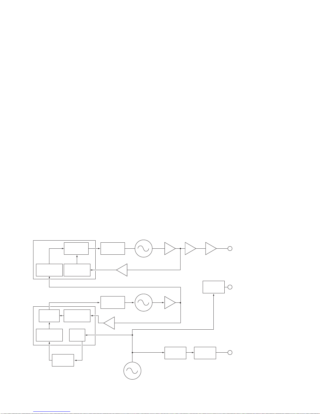
(2) S-METER SQUELCH
The S-meter signal from IC19b is applied to the squelch
comparator (IC19a) to close or open the squelch circuit. The
reference voltage is adjusted by R257 and then applied to
the (–) terminal of the comparator (IC19a). When the S-
meter signal exceeds the reference voltage, the comparator
outputs “High” to the CPU via IC22a and Q46 in the same
manner as the voice activated squelch circuit.
3-2 TRANSMITTER CIRCUITS
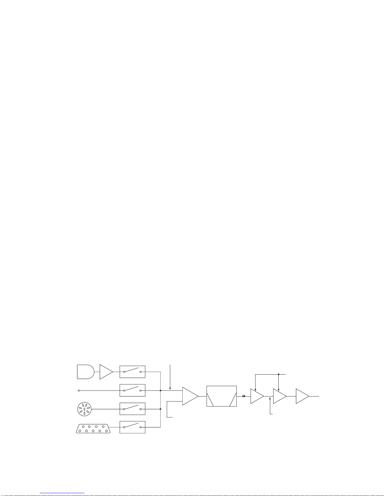
3-2-1 MICROPHONE AMPLIFIER CIRCUIT
(LOGIC BOARD IN THE RC-21)
The AF signals from the [MICROPHONE] connector pass
through the microphone gain controller (R81) and AF ampli-
fier (IC12a), and are applied to the CTRL1 board. The
microphone AGC circuit (D9, D10, Q13, Q14) controls the
amplifier gain to prevent signal distortion.
The AF signals are converted into PWM signal at the PWM
modulation circuit (IC3, Q1, D1) via the AF amplifier (CTRL1
board; IC4), and are applied to the serial interface IC (IC1).
The serial interface IC outputs PWM signal to the CTRL2
board (IC-M710 RT) via a coaxial cable.
The PWM signal from the RC-21 (controller) is applied to the
MAIN unit after being converted into an analog signal by
passing though the serial interface IC on the CTRL2 board.
TheAF signals are applied to the balanced modulator (MAIN
unit; IC9, pin 1) via the AF switch (IC38b).
External modulation inputs from the ACC socket or a 2-tone
emergency signal from the CPU are applied to the balanced
modulator directly via AF switches (IC38, IC39).
3-2-2 MODULATION CIRCUIT (MAIN UNIT)
(1) J3E AND J2B MODES
The balanced modulator is used for J3E and J2B modes to
add the audio signal to the BFO frequency and outputs the
IF signal while suppressing the BFO signal.
The AF signals from the microphone amplifier or external
audio from the modulation terminals are applied to the bal-
anced modulator (IC9, pin 1). The BFO signal from the PLL
unit is applied to IC9 (pin 10) as a carrier signal. A double
sideband signal is output from IC9 (pin 6) and is then applied
to the 9 MHz filter (FI2) to create an SSB signal.
R238 adjusts the balanced level of IC9 for maximum carrier
suppression. In J2B mode, the BFO frequency is shifted 1.7
kHz to set the transmit frequency the same as the displayed
frequency.
The SSB signal from FI2 is amplified at the 9 MHz amplifiers
(Q17–Q19) and is then applied to the mixer circuit (D52).
The switching diode (D19) is turned ON when R8 voltage
disappears.
(2) H3E AND R3E MODES
An SSB signal is applied to the IF amplifier (Q18) in the
same manner as with J3E/J2B mode. The BFO signal from
the PLL unit is amplified at the buffer amplifier (Q30) and is
then applied to the IF amplifier (Q18) as a carrier signal to
be added to an SSB signal. R211 and R212 adjust the car-
rier levels in H3E and R3E modes, respectively.
Microphone IC38b
IC8a 6
1
10 6
5
12
65
IC38a
IC39b
2-tone alarm
NBDP socket
Balance upset during CW, FSK
9.013 MHz carrier
(R3E, H3E only)
CW keying control
(A1A only)
D9 Q19 Q18 Q17
BFO from the PLL unit (MHz)
J3E, R3E, H3E, J2B: 9.013
A1A: 9.0116
FSK: 9.0113 (center)
FSK narrow: 9.0106 (center)
J2B: 9.1023
During tuning: 9.0115
12
IC39a
ACC (1) socket
Crystal
filter
Modulator
IC9 Fl2
• MODULATOR CIRCUIT

3 - 4
(3) A1A AND FSK MODES
The CW8 or FSK8 voltage are applied to the balanced mod-
ulator (IC9, pin 4) to upset the balance and create a carrier
signal.
InA1Amode, the CW keying circuit (IC18a) controls the bias
voltage of the IF amplifiers (Q18, Q19) and T/R switching
diode (D19) to switch the carrier transmission.
In FSK mode, BFO frequency is shifted in the PLL unit to
create the mark and space frequencies.
3-2-3 1ST MIXER CIRCUIT (MAIN UNIT)
The amplified signal from the IF amplifier (Q17) is mixed
with a 60 MHz LO signal at the 1st mixer circuit (D52) to pro-
duce a 69.0115 MHz IF signal. The mixer is commonly used
with the receiver 2nd mixer.
The 69.0115 MHz IF signal passes through the filter (FI1b)
and is then applied to the 2nd mixer circuit.
3-2-4 2ND MIXER CIRCUIT (MAIN UNIT)
The filtered signal is mixed with a PLL output frequency
(1LO: 69.5155–99.0155 MHz) at the 2nd mixer circuit (Q3,
Q4) to produce an RF signal which is the same frequency as
the displayed one.
3-2-5 RF FILTER CIRCUIT (MAIN UNIT)
The RF signal passes through the low-pass filter (L55, L56,
C89–C93, C620, C628) and is then amplified at the RF
amplifier (Q2).
The amplified signal is applied to one of nine RF filters.
These RF filters are commonly used with the receiver circuit
which consists of eight high-pass filters and one low-pass fil-
ter. The filtered signal is amplified at the RF amplifier (Q1)
and is then applied to the PA150W board via J1.
3-2-6 POWER AMPLIFIER CIRCUIT
(PA150W BOARD)
This circuit provides a stable 150 W (at 13.6 V DC) of output
power. The RF signal from the MAIN unit is amplified at the
pre-driver (Q8), driver (Q1, Q2), and power amplifier (Q3,
Q4).
The driver and power amplifiers form class AB push-pull cir-
cuits. Bias voltage to these transistors is produced by diodes
(D1–D3) which have temperature junctions with the transis-
tors.
The amplified signal is then applied to one of eight low-pass
filters to suppress high harmonic components. The filtered
signal passes through the power detector circuit (FILTER
board; L41) and transmit/receive switching relay (FILTER
board; RL17) and is then applied to the antenna connector.
• LOW-PASS FILTERS USED (FILTER BOAED)
3-2-7 ALC CIRCUIT
The transceiver has two ALC (Auto Level Control) loops for
constant output power over all marine bands and for high
power setting.
(1) IF ALC CIRCUIT (MAIN UNIT)
A portion of the IF signals from the IF amplifier (Q17) is
applied to the IF ALC circuit. The signal is amplified at Q126
and then detected at the ALC detector (D46). The detected
signal is amplified at the ALC amplifier (IC17b) and is then
applied to the comparator (IC17a).
Q8 Q1, Q2 Q3, Q4
D9
D10
REF
FOR
L41
Q3, Q4
Q19
Q126
IC17b
IC17a
Q18 Q17 D52
IF ALC CIRCUIT
Q2 Q1
MAIN UNIT PA BOARD FILTER BOARD
Current APC control (Q111)
Low power during tune (Q21, Q22)
High power set (R184)
Low power during tune (Q28)
20 W low power set (Q132)
8 V
IC16b IC16a
–
+
–
+
Q23
RF ALC CIRCUIT
–5 V
Current APC
–
+
• ALC CIRCUIT
Pre-driver Driver
PA
Frequency
(MHz)
0.5–1.999
2–2.999
3–4.999
5–6.999
7–9.999
Frequency
(MHz)
10–13.999
14–17.999
18–19.999
20–21.999
22–23.999
24–29.999
Control
signal
L5
L6
L7
Control
signal
L0
L1
L2
L3
L4
Entrance
coil
RL1
RL3
RL5
RL7
RL9
Entrance
coil
RL11
RL13
RL15

3 - 5
The reference voltage for the comparator is set by R184.
The antenna tuning control voltage (TUN8) is also affected
by the reference voltage to decrease the IF signal level.
The comparator output controls the gate bias of the IF ampli-
fier (Q19), so that the IF signal level is determined by the ref-
erence voltage of the comparator (IC17a).
(2) RF ALC CIRCUIT (FILTER BOARD)
The RF output power level is detected at D9 of the power
detector circuit (L41, D9, D10) on the FILTER board. The
detected signal (“FOR” signal) is applied to the RF ALC
amplifier (IC16a) in the MAIN unit.
The amplified signal enters the transmit gain controller
(IC16b) which functions as an inversion amplifier. The gain
controller decrease the gain of the IF amplifier (Q2) on the
MAIN unit to constant output power from differential amplifi-
er gains which are occurred by their frequency characteris-
tics.
3-2-8 APC CIRCUIT
The APC (Auto Power Control) circuit protects the power
amplifiers on the PA unit from high SWR and excessive cur-
rent.
(1) SWR APC (FILTER BOARD AND MAIN UNIT)
The reflected wave signal appears and increases on the
antenna connector. When the antenna is mismatched, D10
of the power detector circuit (D9, D10, L41) on the FILTER
board detects the signal and applies it to the APC amplifier
(Q23) on the MAIN unit. The output signal decreases the
bias voltage of the RF ALC amplifier to reduce the output
power.
(2) CURRENT APC (PA150W BOARD AND MAIN UNIT)
The power transistor current is detected from the different
voltages between both terminals of a 0.012 Ωresistor (R26)
on the PA150W board. The detected voltage is applied to
the differential amplifier (IC2b). When the current of the final
transistors is more than 30A, the detected voltage is applied
to the APC amplifier controller (Q111) in the MAIN unit to
reduce the gate-2 voltage of the IF amplifier (Q2) and thus
reduce the output power.
3-2-9 TEMPERATURE DETECTION
(PA150W BOARD)
Thermal switches (S1, S2) protect the final transistors from
excessive temperatures. When the temperature of the final
transist (Q4) or exceeds 50 ˚C (122 ˚F), S2 is turned ON to
start the cooling fan. When the temperature of the final tran-
sist (Q3) exceeds 110 ˚C (230 ˚F), S1 is turned ON to con-
trol the “POC2” line and sets the power to 60 W.
3-2-10 RF METER CIRCUIT (MAIN UNIT)
The output of the ALC amplifier (IC16a) is applied to the
CPU (pin 31) to indicate the transmit power level on the dis-
play.
for antenna current meter indication, the “ANTC” signal from
an optional AT-130E is applied to the CPU (pin 32).
PLL IC (IC5)
DDS IC
(IC1)
Main loop VCO Q4
Q3/D4
Reference loop VCO
Q5/D3
Q8
Q11
Q21 Q24
1LO
(69.5115–99.0114 MHz)
Q6
Q2
2LO
(60.0 MHz)
BFO
(9.0106–9.013 MHz)
Reference OSC (X1:30.0 MHz)
Doubler
D/A
convertor
D/A
convertor
DDS
IC2
Loop filter
Loop filter
Phase
detector
Programmable
divider
Programmable
divider
Phase
detector
Programmable
divider
Programmable
divider DDS
• PLL CIRCUIT

3 - 6
3-3 PLL CIRCUIT
3-3-1 GENERAL
The PLL unit generates a 1st LO frequency (69.5115-
99.0114 MHz), 2nd LO frequency (60 MHz) and a BFO fre-
quency (9.0106–9.013 MHz) for the MAIN unit. The 1st LO
PLL adopts a mixerless dual loop PLL system. The BFO
uses a DDS and a 2nd LO as a fixed frequency double that
the crystal oscillator.
3-3-2 1ST LO PLL (PLL UNIT)
The 1st LO PLL contains a main loop and reference loop as
a dual loop system. The reference loop generates a 10.65 to
10.75 MHz frequency using a DDS circuit, and the main loop
generates a 69.5115 to 99.0114 MHz frequency using the
reference loop frequency.
(1) REFERENCE LOOP PLL
The oscillated signal at the reference VCO (Q5, D3) is
amplified at the buffer amplifiers (Q6, Q11) and is then
applied to the DDS IC (IC1, pin 46). The signal is then divid-
ed and detected on phase with the DDS generated frequen-
cy.
The detected signal output from IC1 (pin 56) is converted
into a DC voltage (lock voltage) at the loop filter (R18, R19,
C 44) and then fed back to the varactor diode (D3) in the
VCO circuit.
(2) MAIN LOOP PLL
The oscillated signal at the main loop VCO (Q3, D4) is
amplified at the buffer amplifiers (Q4, Q8) and is then
applied to the PLL IC (IC5, pin 14). The signal is then divid-
ed and detected on phase with the reference loop output fre-
quency.
The detected signal output from IC5 (pins 9, 10) is convert-
ed into a DC voltage (lock voltage) at the loop filter and then
fed back to the varactor diode (D4) in the VCO circuit.
The oscillated signal is amplified at the buffer amplifiers (Q4,
Q21, Q24) and then applied to the MAIN unit as a 1st LO
signal.
3-3-3 2ND LO AND REFERENCE OSCILLATOR
CIRCUITS
The reference oscillator (X1) generates 30.0 MHz frequency
used for the both DDS ICs as a system clock and for the LO
output. The oscillated signal is doubled at the driver (Q2)
and picked up the 60 MHz frequency at the resonator circuit
(L4, L5). The 60 MHz signal is applied to the MAIN unit as a
2nd LO signal.
3-3-4 BFO CIRCUIT
The DDS IC (IC2) generates a 10-bit digital signal using the
30 MHz system clock. The digital signal is converted to an
analog wave signal at the D/A converter (R120–R139). The
analog wave is passed through the low-pass filter (L37, L38,
C154–C158) and is then applied to the MAIN unit as the
BFO signal.
1
10
11
16
17
21
22
23
24
25
26
27
28
30
31
33
34
36
37
39
41
42
48
Input port for the CPU reset signal.
When receiving a “LOW” pulse, the
CPU is reset.
Data input port from the sub CPU in
the controller.
Data output port to the sub CPU in the
controller.
Outputs low power control signal for
60 W power.
Outputs low power control signal for
20 W power.
Outputs a “SEND” control signal for
the ACC socket.
Outputs a “SEND” control signal for T8
and R8 voltage line control.
Low : for transmit.
Outputs an alarm control signal to acti-
vate the 2-tone emergency alarm
encoder.
High : alarm on
Outputs a tone switching signal for the
2-tone emergency alarm encoder.
High : high tone
Outputs a clock signal for the EEP-
ROM (IC46).
IInput port for serial signal from the
EEPROM (IC46).
Outputs serial signal for the EEPROM
(IC46).
Outputs select signal for the EEPROM
(IC46).
Input port for the S-meter indication.
Input port for the RF-meter indication.
Input port for the squelch detected sig-
nal.
High : when squelch is open.
Input port for the transmit/receive
switching signal.
Outputs RF gain control signal to the
AGC circuit.
CW keying input.
High : when key is closed.
Outputs AF gain control signal to the
controller.
Outputs a strobe signal to the main
loop PLL IC (IC5).
Outputs a strobe signal to the refer-
ence loop DDS IC (IC1).
Outputs a strobe signal to the BFO
PLL IC (IC2).
3-4 PORT ALLOCATIONS
3-4-1 CPU (MAIN unit; IC44)
RES
RXDO
TXDO
POC2
POC1
ASEN
CSEN
ALMS
ALMC
SCK
SI
SO
CS
RSM
MFOR
SQLS
TRC
RFG
CWIN
AFG
STB1
STB2
STB3
Pin Port Description
number name

49
50
51
52
53
54
55
57–60
61–64
65–67
68
70
71
72
74
Outputs data to PLL and DDS ICs.
Outputs a clock signal to PLLand DDS
ICs.
Outputs an AF mute signal for squelch
function.
High : squelch closed.
Outputs an external NBDP equipment
control signal.
Low : during NBDP data output
Outputs a “noise blanker” signal.
High : noise blanker is on
Outputs intercom gate control signal.
Outputs a strobe signal for an initial
matrix.
Input ports for an initial matrix.
Output band signals for RF LPF and
BPF selection.
Outputs mode signals.
Input port for an optional AT-130.
Low : during tuning.
Outputs an antenna tuner tuning con-
trol signal for transceiver’s
power/mode control.
Outputs a narrow filter selection sig-
nal.
Low : for an optional narrow filter
selection.
Outputs a program scan control signal
for “AGC fast” and “audio squelch”
deactivation.
Outputs the “ tuner start” pulse to an
optional AT-130.
3 - 7
DATA
CK
SQL C
NBS
AGCS
INC
P20
P17–P14
PD–PA
J2B, R3E,
H3E
KEY
TUNE
FSEL
PROG
STAT
(MAIN unit; IC44)–Continued
Pin Port Description
number name

4 - 1
SECTION 4 ADJUSTMENT PROCEDURES
4-1 PREPARATION BEFORE SERVICING
■REQUIRED TEST EQUIPMENT
EQUIPMENT
DC power supply
RF power meter
(terminated type)
Frequency counter
RF voltmeter
DC voltmeter
Spectram analyzer
GRADE AND RANGE
Output voltage : 13.6 V DC
Current capacity : 30 A or more
Measuring range : 10–200 W
Frequency range : 1.8–30 MHz
Impedance : 50 Ω
SWR : Less than 1.2 : 1
Frequency range : 0.1–100 MHz
Frequency accuracy : ±1 ppm or better
Sensitivity : 100 mV or better
Frequency range : 0.1–100 MHz
Measuring range : 0.01–10 V
Input impedance : 50 kΩ/V DC or better
Frequency minimum : At least 90 MHz
Spectraum bandwidth : 100 kHz or more
EQUIPMENT
Audio generator
Standard signal
generator (SSG)
Oscilloscope
AC millivoltmeter
External speaker
Attenuator
DC ammeter
GRADE AND RANGE
Frequency range : 300–3000 Hz
Measuring range : 1–500 mV
Frequency range : 0.1–30 MHz
Output level : 0.1 µV–32 mV
(–127 to –17 dBm)
Frequency range : DC–100 MHz
Measuring range : 0.01–10 V
Measuring range : 10 mV–10 V
Input impedance : 4 Ω
Capacity : 6 W or more
Power attenuation : 50 or 60 dB
Capacity : 150 W or more
Measurement capability: 1 A/3 A /50 A
‘‘CONNECTIONS
Spectrum
analyzer
Attenuator
50 or 60 dB
DC power supply
13.6 V/30 A to DC power receptacle
to [MICROPHONE]
IC-M710RT
RC-21
[ANT]
to [EXT SP]
[DC 13.6 V]
Audio
generator Pin 7 MICE
[PTT]
6
54
3
Pin 1 MIC
Speaker
• [MICROPHONE] connector (front view)
AC
millivoltmeter
RF power meter
200 W/50 Ω
Standard signal
generator
CAUTION:
DO NOT connect the
signal generator while
transmitting.
DC power supply
13.6 V/3 A
to DC power receptacle
[DC 13.6 V]
Connect pins
3 and 4 for AF
output

4-2 INTERFACE ADJUSTMENTS
4 - 2
INTERFACE
ADJUSTMENT
ADJUSTMENT
ADJUSTMENT ADJUSTMENT CONDITION MEASUREMENT VALUE POINT
UNIT LOCATION UNIT ADJUST
1 • Connect a main body and controller
with a coaxial cable, then turn
power ON.
CTRL2 Connect a frequency
counter to check
point CP2.
1.2672 MHz CTRL2 C22
• CTRL2 BOARD
Interface
check point
Interface
adjustment
CP2
C22

4 - 3
Main loop
lock voltage
adjustment
L24
Main loop
lock voltage
check point
J5
Reference loop
lock voltage
check point
J4
Reference loop
lock voltage
adjustment
C49
Reference
frequency
check point
P2
Reference
frequency
adjustment
L4
L3
L5
• MAIN AND PLL UNITS
4-3 PLL ADJUSTMENTS
REFERENCE
LOOP LOCK
VOLTAGE
MAIN
LOOP LOCK
VOLTAGE
REFERENCE
FREQUENCY
ADJUSTMENT
ADJUSTMENT ADJUSTMENT CONDITION MEASUREMENT VALUE POINT
UNIT LOCATION UNIT ADJUST
1
2
1
2
1
2
• Display frequency : 7.9999 MHz
• Mode : J3E
• Receiving
• Display frequency : 0.0300 MHz
• Display frequency : 0.5000 MHz
• Receiving
• Display frequency : 29.9999 MHz
• Wait for 5 minutes after power ON.
• Terminate P2 on the PLL unit to
ground with a 50 Ωresister.
• Receiving
PLL
PLL
PLL
Connect a digital
multimeter or oscillo-
scope to check point
J4.
Connect a digital
multimeter or oscillo-
scope to check point
J5.
Connect an RF volt-
meter to check point
P2.
Connect a frequency
counter to check
point P2.
3.2 V
More than 1.5 V
4.0 V
More than 1.0 V
Maximum level
(More than +2 dBm)
60.000000 MHz
PLL
PLL
PLL
C49
Verify
L24
Verify
L4, L5
L3

4 - 4
4-4 TRANSMITTER ADJUSTMENTS
IDLING
CURRENT
(For drive
transistors)
(For final
transistors)
IC APC
SWR
DETECTOR
TRANSMIT
PEAK
ADJUSTMENT
ADJUSTMENT ADJUSTMENT CONDITION MEASUREMENT VALUE POINT
UNIT LOCATION UNIT ADJUST
1
2
1
1
2
1
• Display frequency : 12.2300 MHz
• Mode : J3E
• Apply no audio signal to the
[MICROPHONE] connector.
• Transmitting
• Display frequency : 12.2300 MHz
• Mode : J3E
• Apply no audio signal to the
[MICROPHONE] connector.
• Transmitting
• Display frequency : 22.0000 MHz
• Mode : J3E
• Preset R31 on the PA150W board
to the maximum counterclockwise
position.
• Connect a dummy load (10 A)
between lead of R35 (power line)
and EP9 (power ground) on the
PA150W board.
• Connect an audio generator to the
[MICROPHONE] connector and set
as: Frequency : 1.5 kHz
Level : 100 mV rms
• Connect an RF power meter to the
[ANT] connector.
• Transmitting
• Display frequency : 22.0000 MHz
• Mode : J3E
• Ground the lead of R545 on the
MAIN unit with a wire.
• Connect an audio generator to the
[MICROPHONE] connector and set
as: Frequency : 1.5 kHz
• Transmitting
• Display frequency : 12.2300 MHz
• Mode : J3E
• Ground the lead of R545 on the
MAIN unit with a wire.
• Connect an audio generator to the
[MICROPHONE] connector and set
as: Frequency : 1.5 kHz
Level : 3 mV
• Transmitting
PA150W
PA150W
Rear
Panel
Rear
Panel
MAIN
Rear
Panel
Cut the lead wire
(W11) and connect a
DC ammeter (1 A) to
the cut points.
Unsolder R26 and
connect the DC
ammeter (3 A) to the
unsoldered points.
Connect a DC
ammeter (50 A)
between the DC
power supply and DC
power receptacle
(DC input +).
Connect an RF
power meter to the
[ANT] connector.
Connect a DC volt-
meter to R150.
Connect an RF
power meter to the
[ANT] connector.
100 mA
500 mA
30 A
140 W
Minimum level
Maximum output power
PA150W
PA150W
PA150W
Audio
genera-
tor
FILTER
MAIN
R22
R25
R31
Output
level
C92
Adjust in
sequence
L89, L88,
L65, L64,
L59
After adjustment, re-solder the lead wire (W11) on the PA150W board.
After adjustment, re-solder R26 on the PA150W board.
After adjustment, remove the dummy load.
After adjustment, remove the wire from R545 on the MAIN unit.

4 - 5
SWR detector
adjustment
IC APC
preparation
Ammeter
1
45
23
789
DC power
supply
EP9
R35
10 A dummy
load
C92
Idling current
(for final transistors)
adjustment
R25
IC APC adjustment
R31
Idling current
(for final transistors)
check point
Ammeter
R26
EP6
EP4
Ammeter
EP3
Unsolder
Cut W11
R26
Idling current
(for drive transistors)
check point
W11
Idling current
(for drive transistors)
adjustment
R22
Transmit peak
adjustment
SWR detector
check point
R150
L59
L64
L88
L89
L65
SWR detector
transmit peak
preparation
R545
• MAIN UNIT
• PA150W AND FILTER BOARDS

4 - 6
TRANSMITTER ADJUSTMENTS (continued)
TRANSMIT
GAIN
OUTPUT
POWER
CARRIER
SUPPRESSION
TUNE
POWER
POWER
METER
MIC
LIMITTER
MIC GAIN
ADJUSTMENT
ADJUSTMENT ADJUSTMENT CONDITION MEASUREMENT VALUE POINT
UNIT LOCATION UNIT ADJUST
1
2
1
2
3
1
1
1
2
1
1
2
• Display frequency : 12.2300 MHz
• Mode : A1A
• Transmitting
• Display frequency : 16.3650 MHz
• Transmitting
• Display frequency : 12.2300 MHz
• Mode : H3E
• Apply no audio signal to the
[MICROPHONE] connector.
• Transmitting
• Mode : R3E
• Transmitting
• Mode : A1A
• Transmitting
• Display frequency : 12.2300 MHz
• Mode : J3E
• Apply no audio signal to the
[MICROPHONE] connector.
• Transmitting
• Display frequency : 12.2300 MHz
• Ground the lead of L108 (KEY line)
on the MAIN unit with a wire.
• Transmitting
• While pushing the [SQL] and [TX]
switches, turn power ON.
• Display frequency : 12.2300 MHz
• Mode : J3E
• Connect an audio generator to the
[MICROPHONE] connector and set
as: Frequency : 1.5 kHz
Level : 100 mV
• Set the transmit power:
[PO-1] (20 W PEP)
• Transmitting
• Display frequency : 12.2300 MHz
• Mode : J3E
• Preset R81 on the LOGIC board to
the maximum clockwise position.
• Connect an audio generator to the
[MICROPHONE] connector and set
as: Frequency : 1.5 kHz
Level : 150 mV
• Transmitting
• Display frequency : 12.2300 MHz
• Mode : J3E
• Connect an audio generator to the
[MICROPHONE] connector and set
as: Frequency : 1.5 kHz
Level : 10 mV
• Transmitting
• Set an AG as:
Frequency : 1.5 kHz
Level : 5 mV
• Transmitting
140 W
0.5 V
45 W
2.0 W
140 W
Minimum carrier level
(Less than –40 dB)
10 W
17 W
Push the [DIMMER]
switch.
1.5 V PEP
400 mV PEP
100 W
R184
R26
R211
R212
R184
R238
R205
Output
level
[DIMMER]
R91
R81
R883
Rear
Panel
MAIN
Rear
Panel
Rear
Panel
Rear
Panel
Rear
Panel
CTRL2
CTRL2
Rear
Panel
Connect an RF
power meter to the
[ANT] connector.
Connect a digital
multimeter to R159.
Connect an RF
power meter to the
[ANT] connector.
Connect a spectrum
analyzer or RF volt-
meter to the [ANT]
connector via an
attenuator.
Connect an RF
power meter to the
[ANT] connector.
Connect an RF
power meter to the
[ANT] connector.
Connect an oscillo-
scope to check point
CP2 (Refer at page
4-2).
Connect an oscillo-
scope to check point
CP2 (Refer at page
4-2).
Connect an RF
power meter to the
[ANT] connector.
MAIN
MAIN
MAIN
MAIN
Audio
genera-
tor
Font
Panel
LOGIC
LOGIC
MIAN

4 - 7
Transmit gain
check point
Transmit
gain
adjustment
R159
R26
R184
Tune power
preparation
Tune power
adjustment
Mic gain
adjustment
Output power
adjustment
L108
R205
Mic gain
adjustment
R81
R184
R211
R212
R883
Mic limitter
adjustment
R91
Carrier
suppression
adjustment
R238
• MAIN UNIT
• LOGIC BOARD

4 - 8
4-5 RECEIVER ADJUSTMENTS
RECEIVER
GAIN
CLARITY
TOTAL GAIN
S-METER
NOISE
BLANKER
ADJUSTMENT
ADJUSTMENT ADJUSTMENT CONDITION MEASUREMENT VALUE POINT
UNIT LOCATION UNIT ADJUST
1
1
1
2
1
2
1
• Display frequency : 2.1820 MHz
• Mode : J3E
• Noise blanker : OFF
• Squelch : OFF
• Speaker : OFF
• AGC : ON
• RF gain : 9
• R223 (MAIN unit) :
Max. clockwise
• R257 (MAIN unit) : Max.counter
clockwise
• R300 (MAIN unit) : Center
• Connect a standard signal genera-
tor to the [ANT] connector and set
as: Frequency : 2.1815 MHz
Level : 0.5 µV*
(–113 dBm)
Modulation : OFF
• Receiving
• While pushing the [SQL] and [CE]
switches, turn power ON.
• Display frequency : 12.2300 MHz
• Mode : J3E
• Connect a standard signal genera-
tor to the [ANT] connector and set
as: Frequency : 12.2315 MHz
Level : 0.32 mV*
(–57 dBm)
Modulation : OFF
• Receiving
• Set the signal generator to OFF (no
output).
• While pushing the [SQL] and [RX]
switchs, turn power ON.
• Display frequency : 12.2300 MHz
• Mode : J3E
• Connect a standard signal genera-
tor to the [ANT] connector and set
as: Frequency : 12.2315 MHz
Level : 1 mV*
(–47 dBm)
• Receiving
• Display frequency : 12.2300 MHz
• Mode : J3E
• Connect a standard signal genera-
tor to the [ANT] connector and set
as: Frequency : 12.2315 MHz
Level : 3.2 µV*
(–97 dBm)
Add the following signal into
the signal generator output.
• Receiving
Muximum output level
1.0 V
–30 dB (32 mV)
Push the [DIMMER]
switch.
7th dot just appears
while pushing the
[DIMMER].
Adjust the maximum
noise wave displayed
on the oscilloscope.
Adjust in
sequence
L74, L75,
L78, L79,
L83, L84,
L85, L92,
L93
[CLARITY],
[DIMMER]
[VOLUME]
R223
[DIMMER]
Verify
L80, L81
Connect an AC milli-
voltmeter to the [EXT
SP] jack with a 4 Ω
dummy load.
Connect an AC milli-
voltmeter to the [EXT
SP] jack with a 4Ω
dummy load.
S/RF meter
Connect an oscillo-
scope to R59.
MAIN
Front
Panel
Front
Panel
MAIN
Font
Panel
MAIN
Rear
Panel
Rear
Panel
Function
display
MAIN
Set the [CLARITY] control to the center position and
push the [DIMMER] switch.
1234
1 msec.
100 msec.
*This output level of the standard signal generator (SSG) is indicated as SSG’s open circuit.
Other manuals for IC-M710RT
1
Table of contents
Other Icom Transceiver manuals

Icom
Icom IC-F6220D User manual

Icom
Icom IC-M91D Installation and operating instructions

Icom
Icom IC-A24E User manual

Icom
Icom IC-756PROIII User manual

Icom
Icom IC-4088S User manual

Icom
Icom Ic-V88 User manual

Icom
Icom IC-F6012 User manual

Icom
Icom IC-GM651 User manual

Icom
Icom IC-F40GT User manual

Icom
Icom ID-5100A User manual