manuals.online logo
Brands
  1. Home
  2. •
  3. Brands
  4. •
  5. ICS
  6. •
  7. Transceiver
  8. •
  9. ICS PHYceiver ICS1890 Operating and maintenance instructions

ICS PHYceiver ICS1890 Operating and maintenance instructions

Integrated
Circuit
Systems, Inc.
General Description Features
ICS1890
10Base-T/100Base-TX Integrated PHYceiver
ICS1890RevG 10/21/97
Block Diagram
 One chip integrated physical layer
 All CMOS, Low power design (<200mA max)
 Small footprint 64-pin 14mm 2
QFP package
 ISO/IEC 8802-3 CSMA/CD compliant
 Media Independent Interface (MII)
 Alternate 100M stream and 10M 7-wire serial
interfaces provided
 10Base-TX Half & Full Duplex
 100Base-TX Half & Full Duplex
 Fully integrated TP-PMD including Stream
Cipher Scrambler, MLT-3 encoder, Adaptive
Equalization, and Baseline Wander Correction
Circuitry
PHYceiver and QuickPoll are trademarks of Integrated
Circuit Systems, Inc. Patents pending.
The ICS1890 is a fully integrated physical layer device
supporting 10 and 100Mb/s CSMA/CD Ethernet applications.
DTE (adapter cards or motherboards), switching hub, repeater
and router applications are fully supported. The ICS1890
is compliant with the ISO/IEC 8802-3 Ethernet standard
for 10 and 100Mb/s operation.AMedia Independent Interface
allowing direct chip-to-chip connection, motherboard-to-
daughterboard connection or connection via an AUI-like
cable is provided. A station management interface is
provided to enable command information and status
information exchange. The ICS1890 interfaces directly to
transmit and receive isolation transformers and can support
shielded twisted pair (STP) and unshielded twisted pair
(UTP) category 5 cables up to 105 meters. Operation in half
duplex or full duplex modes at either 10 or 100 Mbps
speeds is possible with control by Auto-Negotiation or
manual selection. By employing Auto-Negotiation the
technology capabilities of the remote link partner may be
determined and operation automatically adjusted to the
highest performance common operating mode.
ICS reserves the right to make changes in the device data identified in this publication
without further notice. ICS advises its customers to obtain the latest version of all
device data to verify that any information being relied upon by the customer is current
and accurate.
2
ICS1890
Introduction
The ICS1890 is essentially a nibble/bit stream processor.
When transmitting, it takes sequential nibbles presented at
the Media Independent Interface (MII) and translates them to
aserial bitstream fortransmission onthe media.When receiving,
it takes the serial bit stream from the media and translates it to
sequential nibbles for presentation to the MII. It has no
knowledge of the underlying structure of the MAC frame it is
conveying.
100Base-TX Operation
When transmitting, the ICS1890 encapsulates the MAC
frame (including the preamble) with the start-of-stream and
end-of-stream delimiters. When receiving, it strips off the
SSD and substitutes the normal preamble pattern and then
presents this and subsequent preamble nibbles to the MII.
When it encounters the ESD, it ends the presentation of
nibbles to the MII. Thus, the MAC reconciliation layer sees
an exact copy of the transmitted frame.
During periods when no frames are being transmitted or
received, the device signals and detects the idle condition.
This allows the higher levels to determine the integrity of the
connection. In the 100Base-TX mode, a continuous stream of
scrambled ones is transmitted signifying the idle condition.
The receive channel includes logic that monitors the IDLE
data stream to look for this pattern and thereby establishes
the link integrity.
The 100M Stream Interface option allows access to raw groups
of 5-bit data with lower latency through the PHY.This is useful
in building repeaters where latency is critical.
10Base-T Operation
In 10Base-T mode, the bit stream on the cable is identical to
the de-composed MAC frame. Link pulses are used to establish
the channel integrity. When receiving, the ICS1890 first
synchronizes to the preamble. Once lock is detected, it begins
to present preamble nibbles to the MII. On detection of the
SFD, it frames the subsequent 4-bits which are the first data
nibble.
Configuration
The ICS1890 is designed to be fully configurable using
either hardware pins or the (usually) software-driven MII
Management interface, as selected with the HW/SW pin. A
rich set of configuration options are provided. This allows
diverse system implementations and costs.
3
ICS1890
Modes of Operation
Reset & Basic Initialization
Reset can be accomplished using either register bit 0:15 or the
RESETpin.
For a hardware reset, RESET must be held at a logic zero level
for at least two clock cycles and may be held low as long as
desired.
While RESET is held low the device is in Low Power mode.
After the RESET pin is released to a logic one level, Low
Power mode is exited, the PHY address is latched into register
16, and the reset process continues to completion.
For a software reset, a management agent must write a logic
one to register bit 0:15. This will start the reset process. The
software reset bit will clear itself automatically when reset is
completed.
All reset timing parameters are specified in the Electricals
section of the data sheet.
Low Power and Automatic 100Base-T Power-
Down
The ICS1890 supports two power saving modes. TheICS1890
device can be placed into a state where very littler power is
drawn by the device. This Low Power mode can be activated
by holding the RESET pin continuously low or by writing a
logic one to the Power-down bit (0:11).
When the device is in Low Power mode, all functions are
disabled except for register access through the MII Management
Interface.
All register values are maintained during Low Power mode,
except for latching status bits, which are reset to their default
values.
The ICS1890 can also automatically reduce its total power
requirementswhen operatingin 10Base-Tmodeby automatically
powering-down the 100Base-TX modules.
The power required by the ICS1890 in normal, 100Base-TX
power-down, and Low Power modes is given in the Electricals
section of the data sheet.
Auto-Negotiation
A link can automatically be established using Auto-Negotiation.
When enabled, Auto-Negotiation will exchange information
about the local nodes capabilities with its remote link partner.
After the information is exchanged, each device compares its
capabilities with those of its partner and then the highest
performance operational mode is automatically selected.
As an example, if one device supports 10Base-T and 100Base-
TX, and the other device supports 100Base-TX and 100Base-
T4, 100Base-TX will automatically be selected.
See the Auto-Negotiation section for more details on how the
process is initiated and controlled.
100Base-TX
The primary operational mode of the ICS1890 is to provide
100Base-TX physical layer services. This consists mainly of
converting data from parallel to serial at a 100 Mb/s data rate.
The device may be configured in a number of different ways
and also provides detailed operational status information.
10Base-T
The ICS1890 also provides 10Base-T physical layer services
to allow easy migration from 10 to 100 Mb/s service. Complete
data service is provided with configuration and status available
to management.
Full Duplex
The ICS1890 supports either half and full duplex operation
for both 10Base-T and 100Base-TX. Full Duplex operation
allows simultaneous transmission and reception of data which
can effectively double data throughput to 20 or 200 Mb/s.
To operate in Full Duplex mode, some of the standard 10Base-
T and 100Base-TX behaviors are modified.
In 10Base-T Full Duplex mode, transmitted data is not looped
back to the receiver and SQE test is not performed.
In both 10Base-T and 100Base-TX Full Duplex modes, CRS is
asserted in response only to receive activity and COL always
remains inactive.
4
ICS1890
Interface Overviews
Overview of MAC/Repeater to PHY Interfaces
To accommodate different applications, theICS1890provides
four types of MAC/Repeater to PHY interfaces. The four
interfaces are - 10/100 MII Data Interface, 100M Stream Inter-
face, 10M Serial Interface and the Link Pulse Interface.
The standard and most commonly used interface is the 10/100
MII Data Interface which provides framed 4-bit nibbles and
control signals.
The 100M Stream Interface provides 5-bits of unframed data
as well as the normal CRS signal which can be used as a fast
look-ahead. This interface is intended for 100Base-TX repeater
applications that require nothing more than recovered parallel
data where all framing is handled in the repeater core logic.
The 10M Serial Interface provides a framed single data bit
interface with control signals and is ideally suited to applications
that already incorporate a serial 10Base-T MAC with a standard
7-wire interface.
The Link Pulse Interface is provided for applications that wish
to fully control the Auto-Negotiation process themselves but
not the actual generation and reception of Link Pulses.
MII Data Interface
The ICS1890 implements a fully compliant IEEE 802.3u
Media Independent Interface for connection to MACs or
repeaters allowing connection between the ICS1890 and
MAC on the same board, motherboard/daughter board or via
a cable in a similar manner to AUI connections.
The MII is a specification of signals and protocols which
formalizes the interfacing of a 10/100 Mbps Ethernet Media
Access Controller (MAC) to the underlying physical layer.
The specification is such that different physical media may be
supported (such as 100Base-TX, 100Base-T4 and 100Base-
FX) transparently to the MAC.
The MII Data Interface specifies transmit and receive data
paths. Each path is 4-bits wide allowing for transmission of a
data nibble. The transmit data path includes a transmit clock
for synchronous transfer, a transmit enable signal and a transmit
error signal. The receive data path includes a receive data
clock for synchronous transfer, a receive data valid signal and
a receive error signal. Both the transmit clock and receive
clock are sourced by the ICS1890.
The ICS1890 provides the MII signals carrier sense and
collision detect. In half duplex mode, carrier sense indicates
that data is being transmitted or received, and in full duplex
mode it indicates that data is being received. Collision detect
indicates that data has been received while a transmission is
in progress.
5
ICS1890
The ICS1890 is designed to allow hot insertion of an MII
cable into a MAC MII port. During the power-up phase, the
ICS1890 will isolate the MII and the Twisted Pair Transmit
signal pair
100M Stream Interface
The 100M Stream Interface is an alternative parallel interface
between the PHY and MAC/Repeater than the standard MII
Data interface. The Stream Interface provides a lower level
interface and, therefore, lower bit delay than the standard MII
Data Interface.
This interface is selected by setting the MII/SI pin to STREAM
INTERFACE mode and by setting the 10/100SEL pin to 100
mode.
The Stream Interface bypasses the Physical Coding Sublayer
(PCS) and provides a direct unscrambled, unframed 5-bit
interface to the Physical Media Access (PMA) layer.
The Stream Interface consists of a 14 signal interface: STCLK,
STD[4:0], SRCLK, SRD[4:0], SCRS, SD.
Data is exchanged between the MAC and PHY using 5-bit
unframed code groups at 25 MHz clock rate.
The Stream Interface provides a CRS signal by continuing to
use the logic that is bypassed by this interface. This gives a
carrier indication faster than is possible from the MAC/Repeater
since the bits are examined serially as soon as they enter the
PHY.
Since only the Stream Interface or the MII Interface is active
at once, it is possible to share the MII Data interface pins for
Stream Interface functionality.
The pins have the following mapping:
MII Stream
TXCLK STCLK
TXEN (1)
TXER STD4
TXD3 STD3
TXD2 STD2
TXD1 STD1
TXD0 STD0
RXCLK SRCLK
RXDV (2)
RXER SRD4
RXD3 SRD3
RXD2 SRD2
RXD1 SRD1
RXD0 SRD0
CRS SCRS
COL (3)
LSTA SD
(1) 100Base-TX is a continuous transmission system and the
MAC/Repeater is responsible for sourcing IDLE symbols
when it is not transmitting data when using the Stream Interface.
(2) Since data is not framed when this interface is used, RXDV
has no meaning.
(3) Since the MAC/Repeater is responsible for sourcing both
active and idle data, the PHY can not tell when it is transmitting
in the traditional sense, so no collisions can be detected.
Other mode configuration pins behave identically regardless
of which data interface is used.
6
ICS1890
10M Serial Interface
The 10M Serial Interface is an alternative serial interface
between the PHY and MAC/Repeater than the standard MII
Data interface. The 10M Serial interface provides the same
functionality, but with a serial data stream at a 10 MHz clock
rate.
This interface is selected by setting the MII/SI pin to STREAM
INTERFACE mode and by setting the 10/100SEL pin to 10
mode.
The 10M Serial Interface operation consists of a nine signal
interface:10TCLK, 10TXEN,10TD 10RCLK,10RXDV,10RD,
10CRS, 10COL, and LSTA.
Data is exchanged between the MAC and PHY serially at a 10
MHz clock rate.
Since only the 10M Serial Interface or the MII Interface is
active at once, it is possible to share the MII Data interface
pins for 10M Serial Interface functionality.
The pins have the following mapping:
MII 10M Serial
TXCLK 10TCLK
TXEN 10TXEN
TXER (1)
TXD3
TXD2
TXD1
TXD0 10TD
RXCLK 10RCLK
RXDV 10RXDV
RXER (1)
RXD3
RXD2
RXD1
RXD0 10RD
CRS 10CRS
COL 10COL
LSTA LSTA
(1) Error generation and detection is not supported by
10Base-T.
Other mode configuration pins behave identically regardless
of which data interface is used.
Link Pulse Interface
The Link Pulse Interface is an alternative control interface
between the PHY and MAC/Repeater than the standard MII
Data interface. The Link Pulse provides detailed control over
the Auto-Negotiation process.
This interface is selected by setting the MII/SI pin to STREAM
INTERFACE mode, by setting the 10/100SEL pin to 10
mode, and by setting the 10/LP pin to LP mode.
The Link Pulse Interface consists of a five signal interface:
LTCLK, LPTX, LRCLK, LPRX, SD.
Since only the Link Pulse Interface or the MII Interface is
active at once, it is possible to share the MII Data interface
pins for Link Pulse Interface functionality.
The pins have the following mapping:
MII Link Pulse
TXCLK LTCLK
TXEN
TXER LPTX
TXD3
TXD2
TXD1
TXD0
RXCLK LRCLK
RXDV
RXER LPRX
RXD3
RXD2
RXD1
RXD0
CRS
COL
LSTA SD
Other mode configuration pins behave identically
regardless of which data interface is used.
7
ICS1890
MII Management Interface
The MII also specifies a two-wire management interface and a
protocol between station management and the physical layer.
The ICS1890 implements this interface, providing a
bidirectional data line and a clock input for synchronizing the
data transfers. This interface allows station management to
read from and write to all of the devices registers.
Twisted Pair Interface
TheICS1890is able to operate in either 10Base-T or 100Base-
TX modes using a shared interface to a universal magnetics
module and single RJ-45 connector jack.
The interface signals consist of a differential pair of transmit
signals and a differential pair of receive signals. The interface
also provides pins for setting the 10 & 100M transmit current.
Clock Reference Interface
The ICS1890 synthesizes all its required clock signals from
a single 25MHz frequency reference supplied to the Clock
Reference Interface (REF_IN & REF_OUT).
Any reference must meet the stringent IEEE standard
requirements for total accuracy under all conditions of ±50
parts per million (ppm), even though the device can easily
function with a less accurate reference.
Three reference configurations are supported.
A simple CMOS level signal may be fed into the REF_IN
input, leaving the REF-output unconnected.
A crystal oscillator module may be used to provide the
frequency reference for the REF_IN input instead of simple
reference.
It is possible to use a high precision crystal between the
REF_IN and REF_OUT pins on the ICS1890 to provide the
25MHz time base for part operation. In addition to the
connection of the crystal between these pins, a capacitor
from REF_IN and REF_OUT to ground is necessary to
neutralize the capacitance of the crystal. Since these capacitors
are nominally in series, the values of each of these components
(plus stray board capacitance) will equal twice the rated
capacitance of the crystal (series combination).
It is imperative that the crystal be cut for accuracy and
temperature coeffieients with the equivalent capacitive loading
of the specific board layout and the chosen neutralizing
capacitors. The overall accuracy for ethernet applications
must be ±50ppm total for accuracy, temperature, and aging.
Therefore the crystal must be cut using a fixture with the
equivalent capacitive loading as in the end application. This
custom cutting of the crystal will be at additional cost, but
in high volume applications this may be cost effective compared
to pretuned crystal oscillator modules. For more information,
contact ICS Datacom Applications.
Configuration and Status Interface
This interface provides a full set of pins to allow the device
to be completely configured by hardware.
The interface also provides dynamic tristate control over
both the Twisted Pair Transmit interface and the MII Receive
interface.
Link Status and Stream Cipher Locking status signals are
provided for use by a MAC or custom logic.
PHY Address & LED Interface
The ICS1890 device uses a unique scheme to multiplex the
PHY Address and the LED outputs onto the same set of five
pins.
Simply connecting the LED from the device pin to either
power or ground sets the address bit to a 1 or 0. The device
then uses the address info to drive the LED correctly
independent of its connection. The Pin Description section
provides detailed connection instructions.
8
ICS1890
Functional Blocks
Media Independent Interface (MII) Overview
The MII consists of a data interface, basic register set, and a
serial management interface to the register set.
The data interface is a nibble wide transmit and receive data
interface between the MAC and PHY devices. The interface
supports data transfers at 25 MHz for 100Base-T and 2.5 MHz
for 10Base-T.
The register set consists of basic and extended standard
registers as well as vendor specific registers. There are two
basic registers, a control register to handle basic device
configuration, and a status register to report basic device
abilities and status. The standard extended registers provide
access to an Organizationally Unique Identifier and Auto-
Negotiation functionality.
The ICS1890 also provides vendor specific registers that
enhance the device operation. Among these is the QuickPoll
Detailed Status register which provides a comprehensive set
of real-time device information with only single register access.
Auto-Negotiation
The auto-negotiation logic of the ICS1890 has three main
purposes. Firstly, to determine the capabilities of the remote
partner (device at the other end of the cable). Secondly, to
advertise its own capabilities to the remote partner.And thirdly,
to establish a connection with the remote partner using the
highest performance common connection technology.
The ICS1890 auto-negotiation logic is designed to operate
with legacy 10Base-T networks or newer systems with multiple
connection technology options. When operating with a legacy
10Base-T remote partner, theICS1890will select the 10Base-
T operating mode transparently to the remote partner thus
allowing the preservation of existing legacy network structures
without management intervention.
Auto-negotiation is accomplished using a physical signaling
scheme that is transparent at the packet and higher level
protocols. This scheme builds upon the 10Base-T link test
pulse sequence by using a burst of pulses to signal
configuration information between the two devices.
The Fast Link Pulse Bursts are simultaneously exchanged by
both nodes on a link segment the local node encodes the data
from the Auto-negotiation Advertisement Register (register
4) into the FLP Bursts it transmits. The data received from the
link partners FLP Bursts is placed into the Auto-Negotiation
LinkPartner AbilityRegister(register 5).WhenAuto-Negotiation
is complete (1:5=1 or 17:4=1), the highest priority technology
from the following table that is common in the two registers is
automatically selected as the operating mode.
Priority ResolutionTable
Highest Priority Listed first.
1) 100Base-TX FullDuplex
2) 100Base-T4
3) 100Base-TX
4) 10Base-T Full Duplex
5) 10Base-T
9
ICS1890
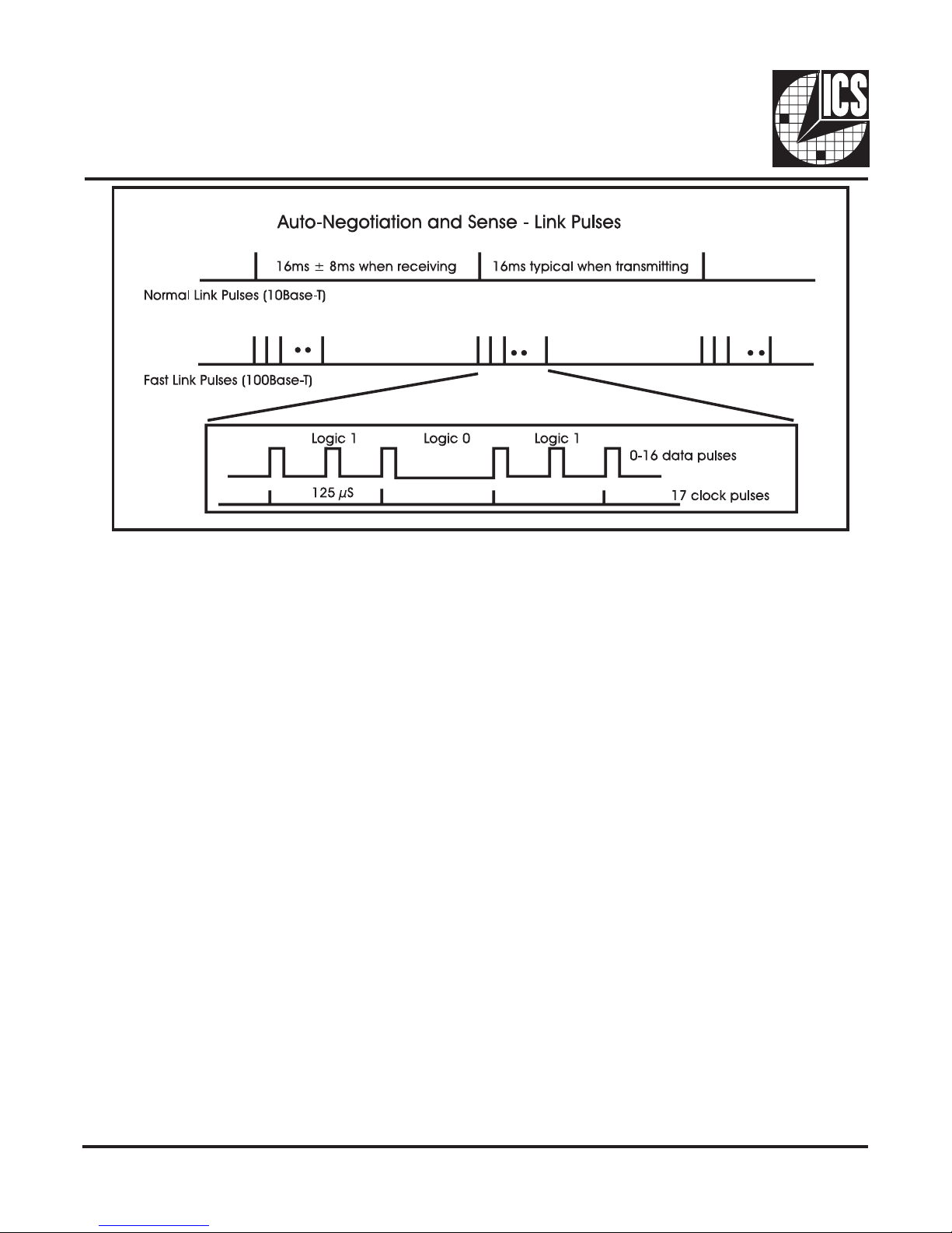
In the event that the link partner does not support auto-
negotiation, backward compatibility is guaranteed because
legacy systems will not respond to the burst (called Fast Link
Pulses). 10Base-T systems will continue to send 10Base-T
link test pulses which will be interpreted by the ICS1890 as
a 10Base-T technology only device. 100Base-TX systems
would send scrambled idle symbols, which would be interpreted
by theICS1890as a 100Base-TX only device. Auto-negotiation
is invoked at power-up, upon request by management, or
manually.
Auto-Negotiation Progress Monitor
Under normal circumstances, Auto-Negotiation is able to
effortlessly establish a connection with the link partner. There
are, however, some situations that may prevent Auto-
Negotiation from completing properly. TheAuto-Negotiation
Progress Monitor is designed to provide detailed information
to a station management entity to assist it in making a connection
in the event that Auto-Negotiation is unable to establish a
connection by itself.
During normal Auto-Negotiation operation, the device ex-
changes capability information with its link partner and then
sets the Auto-Negotiation Complete bit in the Status register
(1:5) (also available in the QuickPoll register as bit 17:4) to a
logicone toindicate thatthe informationexchange hascompleted
successfully and that Auto-Negotiation has handed off the
link startup process to the negotiated technology.
Auto-Negotiation can also accommodate legacy 10Base-T
and100Base-TX linkpartners thatdo nothave Auto-Negotiation
capability. In this case, Auto-Negotiation identifies the link
partner as not being Auto-Negotiation able by setting the
LP_AutoNeg_Able bit (6:0) to a logic zero, identifies the
legacy connection to be made by setting the single bit
corresponding to that technology in the AN Link Partner
Abilities Register (either bit 5:7 or 5:5), and finally indicates
Auto-Negotiation Complete.
The entire process, in either case, usually takes less than half
a second to complete. Typically, management will poll the
Auto-Negotiation Complete bit and then the Link Status bit to
determine when a connection has been successfully made
and then the actual type of connection can be determined by
management. This information is all contained in the QuickPoll
register.
When Auto-Negotiation fails, Auto-Negotiation Complete may
never become true or Link Status may never become good.
Station management can detect this condition and discover
why there is a failure to connect by using the detailed information
provided by the Auto-Negotiation Progress Monitor.
The Auto-Negotiation Progress Monitor provides four bits of
status in the QuickPoll Detailed Status register when combined
with the already present Auto-Negotiation Complete bit.
As progress is made through the Auto-Negotiation Arbitration
state machine, higher status values are locked in to the progress
monitor. The status value only is allowed to increase until
either Auto-Negotiation is completed successfully or the
progress monitor status is read by management.
After the status is read by management, the status is reset to
the current status of the Arbitration state machine. After
negotiation has completed successfully, any link failure will
cause the process to being anew.
This behavior allows management to always determine the
greatest forward progress made by the Auto-Negotiation logic.
Status Progress Monitor Status Bits
A-N Complete Bit 2 Bit 1 Bit 0
Idle 0000
Parallel Detected 0 0 0 1
Parallel Detection Failure 0 0 1 0
Ability Matched 0 0 1 1
Acknowledge Match Failure 0 1 0 0
Acknowledge Matched 0 1 0 1
Consistency Match Failure 0 1 1 0
Consistency Matched 0 1 1 1
Auto-Negotiation Completed Successfully 1 1 1 1
10
ICS1890
100Base-TX Physical Coding Sublayer [PCS]
Carrier Detector & Framer
The carrier detector examines the serial bit stream looking for
the SSD, the JK symbol pair. In the idle state, IDLE symbols
(all logic ones) will be received. If the carrier detector detects a
logic zero in the bit stream, it examines the following bits
looking for the first two non-contiguous zeros, confirms that
the first 5-bits form the J symbol (11000) and asserts carrier
detect. At this point the serial data is framed and the second
symbol is checked to confirm the K symbol (10001). If
successful, the following framed data (symbols) are presented
to the 4B5B decoder. If the JK pair is not confirmed, the false
carrier detect is asserted and the idle state is re-entered.
Collision Detector Collision is asserted in half-duplex
mode when transmission and data reception occur
simultaneously. In full duplex mode, collision is never asserted.
Parallel/Serial Converter
This block converts data between 5-bit symbols and 1-bit
serial data.
4B/5B Encoder/Decoder
When the ICS1890 is operating in the 100Base-TX mode,
4B5B coding is used. This coding scheme maps a 4-bit nibble
to a 5-bit code group. Since this gives 32 possible symbols
and the data only requires 16 symbols, 16 symbols are designated
control or invalid. The control symbols used are JK as the
start-of-stream delimiter (SSD), TR as the end-of-stream
delimiter (ESD), I as the IDLE symbol and H to signal an
error.All other symbols are invalid and, if detected, will set the
receive error bit in the status register.
When transmitting, nibbles from the MII are converted to 5-
bit code groups. The first 16 nibbles obtained from the MII are
the MAC frame preamble. TheICS1890 replaces the first two
nibbles with the start-of-stream delimiter (the JK symbol
pair). Following the last nibble, theICS1890 adds the end-of-
stream delimiter (the TR symbol pair).
When receiving, 5-bit code groups are converted to nibbles
and presented to the MII. If the ICS1890 detects one or more
invalid symbols, it sets the receive error bit in the status
register. When receiving a frame, the first two 5-bit code
groups received are the start-of-stream delimiter (the JK
symbol pair), the ICS1890 strips them and substitutes two
nibbles of the normal preamble pattern. The last two 5-bit code
groups are the end-of- stream delimiter (the TR symbol
group), these are stripped from the nibbles presented to the
MAC.
11
ICS1890
Symbol Meaning 4B Code
3210 5B Code
43210
0 Data 0 0000 11110
1 Data 1 0001 01001
2 Data 2 0010 10100
3 Data 3 0011 10101
4 Data 4 0100 01010
5 Data 5 0101 01011
6 Data 6 0110 01110
7 Data 7 0111 01111
I Idle undefined 11111
J SSD 0101 11000
K SSD 0101 10001
T ESD undefined 01101
R ESD undefined 00111
H Error undefined 00100
V Invalid undefined 00000
V Invalid undefined 00001
4B5B Encoding (including invalid test mode coding)
Symbol Meaning 4B Code
3210 5B Code
43210
8 Data 8 1000 10010
9 Data 9 1001 10011
A Data A 1010 10110
B Data B 1011 10111
C Data C 1100 11010
D Data D 1101 11011
E Data E 1110 11100
F Data F 1111 11101
V Invalid undefined 00010
V Invalid undefined 00011
V Invalid undefined 00101
V Invalid undefined 00110
V Invalid undefined 01000
V Invalid undefined 01100
V Invalid undefined 10000
V(S) Invalid undefined 11001
Invalid Error Code Test (TXER asserted)
V Invalid 0 0 1 0 0 0 0 1 0
V Invalid 0 0 1 1 0 0 0 1 1
V Invalid 0 1 0 1 0 0 1 0 1
V Invalid 0 1 1 0 0 0 1 1 0
V Invalid 1 0 0 0 0 1 0 0 0
V Invalid 1 0 1 0 0 1 1 0 0
V Invalid 1 1 0 0 1 0 0 0 0
V(S) Invalid 1 1 0 1 1 1 0 0 1
I Idle 1 1 1 1 1 1 1 1 1
J SSD 1 1 1 0 1 1 0 0 0
K SSD 1 0 1 1 1 0 0 0 1
T ESD 1 0 0 1 0 1 1 0 1
R ESD 0 1 1 1 0 0 1 1 1
H Error 0 1 0 0 0 0 1 0 0
V Invalid 0 0 0 0 0 0 0 0 0
V Invalid 0 0 0 1 0 0 0 0 1
12
ICS1890
100Base-T Physical Media Access [PMA]
Clock Recovery
The Clock Recovery block locks onto the incoming data stream,
extracts the embedded clock, and presents the data synchronized
to the recovered clock. This process produces signals with
very low timing uncertainty and noise (jitter).
In the event that the PLL is unable to lock on to the receive
signal, it generates a not locked signal. The transmit clock
synthesizer provides a center frequency reference for operation
of the clock recovery circuit in the absence of data. The
receive signal detected and not locked signals are both
used by the logic which monitors the receive channel for
errors.
Transmit Clock Synthesizer
The ICS1890 synthesizes the transmit clock using a PLL to
produce 2.5 MHz for 10Base-T and 25 MHz for 100Base-TX.
Internal clock frequencies of 20 MHz and 125 MHz are also
generated. This allows the use of a low cost 25 MHz crystal
oscillator for a low jitter reference frequency.
Signal Detector
The ICS1890 Signal Detector is part of the clock recovery
PLL. It detects a Receive Signal Error if no receive signal is
received and detects a PLL Lock Error if the PLL is unable to
lock on to the receive channel signal. A receive channel error
is defined as the loss of receive signal or the loss of PLL lock.
Remote Fault Signaling Remote fault signaling allows a
link partner to signal receive channel errors on its transmit
channel. It is then possible to establish the integrity of both
the transmit and receive channels. If auto-negotiation is enabled,
the ICS1890 monitors the receive channel for Fast Link
Pulses or Normal Link Pulses. If an error is detected, the
remote error condition is signaled.
The ICS1890 is able to report a remote fault detected by its
link partner. When the link partner is an ICS1890, a remote
fault will be signaled when it detects a receive signal error.The
definition of a remote fault for a non-ICS1890 link partner is
undefined, but generally will mean that there is a problem with
the integrity of the link partners receive channel.
13
ICS1890
Figure 2
0.1 1 10 100
0
2
4Resistance (Ohm/m) v. Freq. (MHz)
100Base-T Twisted Pair Physical Media
Dependent [TP-PMD]
Stream Cipher Scrambler/Descrambler
When the ICS1890 is operating in the 100Base-TX mode, a
stream cipher scrambler/descrambler that conforms to the ANSI
Standard X3T9.5 FDDI TP-PMD is employed. The purpose of
the stream cipher scrambler is to randomize the 100 Mbps data
on transmission resulting in a reduction of the peak amplitudes
in the frequency spectrum. The stream cipher descrambler
restores the received 5-bit code groups to their unscrambled
values. The stream cipher scrambler/descrambler is bypassed
in the 100M stream interface mode.
MLT-3 Encoder/Decoder
When the ICS1890 is operating in the 100Base-TX mode, an
MLT-3 encoder and decoder is employed.The encoder converts
the NRZI transmitted bit stream to a three-level code resulting
in a reduction in the energy over the critical frequency range
of20MHz to100MHz.The MLT-3 decoderconverts thereceived
three-level code back to an NRZI bit stream.
DC Restoration
The 100Base-TX specification uses a stream cipher scrambler
to minimize peak amplitudes in the frequency spectrum.
However, the nature of the stream cipher and MLT-3 encoding
is such that long run lengths of zeroes and ones can cause the
production of a DC component. This DC component cannot
be transmitted through the isolation transformers and results
in baseline wander. Baseline wander decreases noise immunity
since the base-line moves closer to either the positive or
negative signal comparaters. Figure 1 is an exaggerated
simulation of the effect of baseline wander (the time period
would normally be much longer).
The ICS1890 uses DC restoration to restore the lost DC
component of the recovered digital data thus correcting for
baseline wander.
Adaptive Equalizer
The ICS1890 includes an adaptive equalizer to compensate
for signal amplitude and phase distortion incurred from the
transmission media. Signal equalization will actively occur for
twisted pair cable lengths of up to 105 meters.
At a data rate of 100 Mbps, the cable introduces significant
signal distortion due to high frequency roll off and phase
shift. The high frequency loss is mainly due to skin-effect
which causes the conductor resistance to rise as the square of
the frequency (see Figure 2).
Figure 1
14
ICS1890
0.1 1 10 100
30
20
10
0
typical
worst case
Cable Attenuation (dB) v. Freq. (MHz)
Figure 3
Figure 4
Typical and worst case frequency response for 100 meters
(worst case length as derived from draft standard EIA/TIA-
568- A) of UTP Category 5 cable is shown in Figure 3.
The pulse shape of the received signal is critical for MLT-3
encoded data since there are three distinct levels to resolve in
order to properly recover the data. Figure 4 shows the typical
signal at the input and output ends of 100 meters of UTP
Category 5 cable.
Since the cable length that must be equalized can be anything
from 0 to 105 meters, the optimum equalization cannot be fixed,
but must depend on cable length. Thus, adaptive equalization
must be applied at the receive end to restore the signal.
Theadaptive equalizationprocess consistsof applyingincreasing
amounts of phase and gain correction while monitoring the
integrity of the recovered data. The adaptive equalizer picks
the best of 32 equalization settings and Fixes this value into
the equalization register.This setting provides the best recovery
of the transmitted data with lowest Bit Error Rate (BER).
LineTransmitter The line transmitter logic of theICS1890
is a current-driven differential driver which can be programmed
for either two-level (10Base-T, Manchester) or three-level
(100Base-TX, MLT-3) transmission. Waveshaping is applied
to control the output edge rate and eliminate the need for
expensive external filters. The transmitter interfaces directly to
an inexpensive isolation transformer (magnetics).
Line Receiver The line receiver circuit accepts either a
differential two-level (10Base-T, Manchester) or three-level
(100Base-TX, MLT-3) signal which first passes through an
isolationtransformer.Ifthe polaritycorrectbit intheConfiguration
Register is asserted, the ICS1890 has sensed the reversed
polarity of the receive pair and can switch polarity automatically.
MagneticsA Universal Magnetics module is used to provide
isolation and signal coupling onto the twisted pair cabling for
both 10Base-T and 100Base-TX.
15
ICS1890
10Base-T Block Diagram
10Base-T
Manchester Encoder/Decoder
When the ICS1890 is operating in the 10Base-T mode,
Manchester coding is used. When transmitting, nibbles from
the MII are converted to a serial bit stream and then Manchester
en-coded. When receiving, the Manchester encoded bit stream
is decoded and converted to nibbles for presentation to the
MII.
Clock Synthesis
A 2.5 MHz clock is synthesized for nibble wide transactions.
A 10 MHz clock is synthesized for serial transactions.
Clock Recovery
The PLL synchronizes on the MAC frame preamble and then
begins recovering data normally.
Idle Function
The Idle function is used to keep a 10Base-T link alive in the
absence of data transmission.
If no data traffic is transmitted for 16ms, a link pulse will be
transmitted. Link pulse transmission will continue every 16ms
until real data is transmitted.
Link Monitor
This function is used to qualify a 10Base-T link. If neither data
or a Link Pulse is received for 50 to 150ms, then the link is
considered down. This state is exited after data is received or
3 to 10 Link Pulses are received.
16
ICS1890
Carrier Detector
In half duplex mode carrier is asserted during transmission or
reception of data. In full duplex or repeater mode, carrier is
asserted only on reception of data.
Collision Detector
Collision occurs whenever there is simultaneous transmit
and receive activity when a half duplex link is established.
Collision never occurs in full duplex mode.
Jabber
The Jabber function prevents the transmitter from erroneously
transmitting for too long a period. The maximum time the
device should transmit continuously is the time it takes to
send a maximum length packet (1500 bytes). The Jabber
function ensures that transmission lasts no longer than 20-
150ms. The typical value for the ICS1890 is 21ms.
When the jabber timer is exceeded, Collision (COL) is
asserted and the transmit output goes idle for 0.5 ±0.25s.
This function can be disabled with the Jabber Inhibit register
bit (18:5).
SQETest
This test is only used in Half Duplex DTE applications and is
disabled in repeater and Full Duplex mode. This test can also
be disabled with the SQE Test Inhibit register bit (18:2).
When enabled and a link is established, 0.6 to 1.6us after the
last positive transition of a transmitted packet, COL will be
asserted for 10 ±5 bit times.
Manchester Encoder/Decoder
When the ICS1890 is operating in the 10Base-T mode,
Manchester coding is used. When transmitting nibbles from
the MII are converted to a serial bit stream and then Manchester
en-coded. When receiving, the Manchester encoded bit stream
is decoded and converted to nibbles for presentation to the
MH.
Clock Synthesis
A 2.5MHz clock is synthesized for nibble wide transactions.
A 10MHz clock is synthesized for serial transactions.
Clock Recovery
The PLL synchronizes on the MAC fram preamble and then
begins recovering data normally.
Squelch
The squelch function qualifies the data coming into the device
so that spurious noise events are rejected.
Auto Polarity Correction
By examining the polarity of received Link Pulses theICS1890
can determine if the two wires in the receive data pair were
wired correctly. If the wires were accidentally reversed during
installation, the Auto Polarity Correction function can
automatically correct this in the ICS1890. If the ICS1890
corrects the polarity, this is reflected in the 10Base-TOperations
register. This function can also be disabled through the same
register, if desired.
Line Transmitter
The line transmitter logic of the ICS1890 is a current-driven
differential driver which can be programmed for either two-
level(10Base-T,Manchester) orthree-level (100Base-TX,MLT-
3) transmission. Wavespaping is applied to control the output
edge late and eliminate the need for expensive external filters.
The transmitter interfaces directly to an inexpensive isolation
transformer (magnetics).
Line Receiver
The line receiver circuit accepts either a differential two-level
(10Base-T, Manchester) or three-level (100Base-TX, MLT-3)
signal which first passes through an isolation transformer. If
the polarity correct bit in the Configuration Register is asserted,
the ICS1890 will sense the polarity of the receive pair and, if
necessary, switch polarity automatically.
Magnetics
A Universal Magnetics module is used to provide isolation
and signal coupling onto the twisted pair cabling for both
10Base-T and 100Base-TX.
17
ICS1890
Management Interface
The ICS1890 provides a management interface to connect to
a management entity. The two wire serial interface is part of
the MII and is described in the MII section. The interface
allows the transport of status information from the ICS1890
tothe managemententity andthe transportof controlinformation
to the ICS1890. It includes a register set, a frame format, and
a protocol.
Management Register Set
The register set includes the mandatory basic control and
status registers and an extended set. TheICS1890implements
the following registers.
Control (register 0)
Status (register 1)
PHYIdentifier (register 2)
PHYIdentifier (register 3)
Auto-Negotiation Advertisement (register 4)
Auto-Negotiation Link Partner Ability (register 5)
Auto-Negotiation Expansion (register 6)
Reserved by IEEE (registers 7-15)
Extended Control (register 16)
QuickPoll Status (register 17)
10Base-T Operations (register 18)
Extended Control 2 (register 19)
Reserved by ICS (registers 20-31)
Management Frame Structure
The management interface uses a serial bit stream with a
specified frame structure and protocol as defined below.
Preamble 11...11 (32 ones)
SOF 01 (2 bits)
Op Code 10(read), 01 (write) (2 bits)
Address AAAAA (5bits)
Register RRRRR (5 bits)
TA NN (2 bits)
Data DD...DD (16 bits)
Idle Zo high impedance
Preamble
The ICS1890 looks for a pattern of 32 logic ones followed by
the SOF delimiter before responding to a transaction.
Start of Frame
Following the preamble a start of frame delimiter of zero-one
initiates a transaction.
Operation Code The valid codes are 10 for a read operation
and 01 for a write operation. Other codes are ignored.
Address
There may be up to 32 PHYs attached to the MII. This 5 bit
address is compared to the internal address of the ICS1890,
as set by the P[0...4]* pins, for a match.
Register Address
The ICS1890 uses this field to select one of the registers
within the set. If a non-existent register is specified, the
ICS1890 ignores the command.
TA
This 2-bit field is used by the ICS1890 to avoid contention
during read transactions. TheICS1890will remain in the high
impedance state for the first bit time and drive a logic zero for
the second bit time.
Data
This is a 16-bit field with bit 15 being the first bit sent or
received.
Idle
The ICS1890 is in the high impedance state during the idle
condition. At least one idle must occur after each write to the
device. No idles are required after a read.
18
ICS1890
Register Access Rules
RO - Read Only, writes ignored
CW - Command OverrideWritable
RW/0 - Read/Write only logic zero
RW - Read/Write
Four types of register access are supported by the device.
Read Only (RO) bits may be read, but writes are ignored.
Command OverrideWritable (CW) bits may be read, but writes
are ignored unless preceded by writing a logic one to the
Command Register Override bit (16:15). ReadWrite Zero (RW/
0) bits may be read, but must only be written with a logic zero
value. Writing a logic one to this type of bit may prevent the
device from operating normally. ReadWrite (RW) bits may be
read and may be written to any value.
Default Values
- - No default value
0 - Default to logic zero
1 - Default to logic one
Pin - Default depends on the state of the
name named pin
Modifier
SC - Self Clearing
LL - Latching Low
LH - Latching High
Self clearing bits will clear without any further writes after a
specified amount of time. Latching bits are used to capture an
event. To obtain the current status of a latching bit, the bit
must be read twice in succession. If the special condition still
persists, the bit will be the same on the second read; otherwise,
the condition indication will not be present.
19
ICS1890
Control Register (register 0 [0x00])
Control Register (register 0)
The control register is a 16-bit read/write register used to set
the basic configuration modes of the ICS1890. It is accessed
through the management interface of the MII.
Reset (bit 15)
Setting this bit to a logic 1 will reset the device and result in
the ICS1890 setting all its status and control registers to their
default values. During this process the ICS1890 may change
internal states and the states of physical links attached to it.
While in process, the bit will remain set and no other write
commands to the control register will be accepted. The reset
process will be completed within 500 ms and the bit will be
cleared indicating that the reset process is complete.
Loop Back (bit 14)
Setting this bit to a logic one causes the ICS1890 to tristate
the transmit circuitry from sending data and the receive circuitry
from receiving data. The collision detection circuitry is also
disabled unless the collision test command bit is set. Data
presented to the MII transmit data path is returned to the MII
receive data path. The delay from the assertion of Transmit
Data Enable (TXEN) to the assertion of Receive Data valid
(RXDV) will be less than 512 bit times.
Bit Definition When bit=0 When bit=1 Access Default Hex
15 Reset no effect reset the PHY RW/SC 0
3
14 Loopback disable loop back mode enable loop back mode RW 0
13 Data Rate 10 Mb/s operation 100 Mb/s operation RW 1
12 Auto-Negotiation Enable disable Auto-Negotiation enable Auto-Negotiation RW 1
11 Power-Down normal mode reduced power
consumption RW 0
0*
10 Isolate no effect isolate PHY from MII RW
0 if PHY
Address > 0
1 if PHY
Address=0
9 Restart Auto-Negotiation no effect restart Auto-Negotiation RW 0
8 Duplex Mode half duplex full duplex RW 0
7 Collision Test no effect enable collision signal test RW 0
0
6 Reserved always 0 RO 0
5 Reserved always 0 RO 0
4 Reserved always 0 RO 0
3 Reserved always 0 RO 0
0
2 Reserved always 0 RO 0
1 Reserved always 0 RO 0
0 Reserved always 0 RO 0
20
ICS1890
Data Rate (bit 13)
If Auto-Negotiation is disabled, setting this bit to a logic one
causes the ICS1890 to operate in the 100 Mbps mode only
and setting this bit to a logic zero causes it to operate in the 10
Mbps mode only. If Auto-Negotiation is enabled, this bit, if
read, has no meaning and, if written, has no effect on the
ICS1890operation. Thisbit alsohas nomeaningwhen Hardware
Priority mode is selected with the HW/SW pin. The status of
theHW/SW pinis reflectedin registerbit 19:14.When Hardware
Priority mode is selected, the 10/100SEL pin sets the speed.
The Data Rate status bit in the QuickPoll register (17:14)
always shows the correct setting of an active link.
Auto-Negotiation Enable (bit 12)
Setting this bit to a logic one causes theICS1890 to determine
the link configuration using the auto-negotiation process.
This will be accomplished by the ICS Auto-Negotiation logic
and the state of the Data Rate (bit 13) and the Duplex Mode
(bit 8) will be ignored. Setting this bit to a logic zero will cause
the link configuration to be determined by bits 8 & 13 or the
DPXSEL & 10/100SEL pins as selected by the HW/SW pin.
This bit has no meaning when Hardware Priority mode is
selected with the HW/SW pin. In this case, the ANSEL pin
controls Auto-Negotiation use.
Power-Down (bit 11)
Setting this bit to a logic zero has no effect on the ICS1890.
Setting it to logic one will cause the ICS1890 to isolate its
transmit data output and its MII interface with the exception
of the management interface. The ICS1890 will then enter a
Low Power mode where only the management interface and
logic remain active. Setting this bit to logic zero after it has
been set to a logic one will cause theICS1890 to power-up its
logic and then reset all error conditions. It then enables transmit
data and the MII interface.
Isolate (bit 10)
Setting this bit to a logic one causes the ICS1890 to isolate
its data paths from the MII. In this mode, sourced signals
(TXCLK, RXCLK, RXDV, RXER, RXD0-3, COL and CRS)
are in a high impedance state and input signals (TXD0-3,
TXEN and TXER) are ignored. The management interface is
unaffected by this command.
Restart Auto-Negotiation (bit 9)
Setting this bit to a logic one causes the ICS1890 to restart
auto-negotiation. Upon initiation, this bit will be reset to zero.
Setting this bit has no effect if auto-negotiation is not enabled.
Duplex Mode (bit 8)
If Auto-Negotiation is disabled, setting this bit to a logic one
causes the ICS1890 to operate in the full duplex mode and
setting this bit to a logic zero causes it to operate in the half
duplex mode. If Auto-Negotiation is enabled, this bit, if read,
has no meaning and, if written, has no effect on the ICS1890
operation. This bit also has no meaning when Hardware Priority
mode is selected with the HW/SW pin. In this case, the DPXSEL
pin sets the duplex mode. If the ICS1890 is operating in loop
back mode, this bit will have no effect on the operation.
Collision Test (bit 7)
This command bit is used to test that the collision circuitry is
working when the ICS1890 is operating in the loop back
mode. Setting this bit to a logic one causes the ICS1890 to
assert the collision signal within 512 bit times of TXEN being
asserted and to de-assert it within 4-bit times of TXEN being
de-asserted. Setting this bit to a logic zero causes theICS1890
to operate in the normal mode.
Reserved (Bits 6 through 0)
These bits are reserved for future IEEE standards. When read,
logic zeros are returned. Writing has no effect on ICS1890
operation.

Popular Transceiver manuals by other brands

Garmin GDR 66 Installatioin manual

Garmin

Garmin GDR 66 Installatioin manual

Apache Labs ANAN-100/D manual

Apache Labs

Apache Labs ANAN-100/D manual

Yaesu FT DX 3000 operating manual

Yaesu

Yaesu FT DX 3000 operating manual

Uniden UH8060S owner's manual

Uniden

Uniden UH8060S owner's manual

Yeticomnz Optima user manual

Yeticomnz

Yeticomnz Optima user manual

Yaesu FTM-100DR/DE operating manual

Yaesu

Yaesu FTM-100DR/DE operating manual

Kenwood TK-2140 Mode d'emploi

Kenwood

Kenwood TK-2140 Mode d'emploi

FlexRadio Systems FLEX-5000A quick start guide

FlexRadio Systems

FlexRadio Systems FLEX-5000A quick start guide

Kenwood TS-120S Service manual

Kenwood

Kenwood TS-120S Service manual

Vertex Standard VX-456 operating manual

Vertex Standard

Vertex Standard VX-456 operating manual

Alinco DR-138 Information

Alinco

Alinco DR-138 Information

Yaesu FTDX5000D HF - PRODUCT REVIEW 12-2010 manual

Yaesu

Yaesu FTDX5000D HF - PRODUCT REVIEW 12-2010 manual

Alinco DX-77T user guide

Alinco

Alinco DX-77T user guide

Yaesu FTM-300DR operating manual

Yaesu

Yaesu FTM-300DR operating manual

ADTRAN 3060 Installation and Maintenance

ADTRAN

ADTRAN 3060 Installation and Maintenance

Cactus V5 user manual

Cactus

Cactus V5 user manual

MDS 2710D Installation & operation guide

MDS

MDS 2710D Installation & operation guide

Kenwood NX-740H instruction manual

Kenwood

Kenwood NX-740H instruction manual

manuals.online logo
manuals.online logoBrands
  • About & Mission
  • Contact us
  • Privacy Policy
  • Terms and Conditions

Copyright 2025 Manuals.Online. All Rights Reserved.