IDT P9038 User manual

APPLICATION NOTE
AN-894 08/23/15 1 ©2015 Integrated Device Technology, Inc.
P9038 Layout Guide AN-894
Contents
(Click on any of the headings below to jump to that section)
Using the Reference Layout ................................................................................................................2
Importing the Reference Layout .................................................................................................................. 2
Connecting a Power Source ......................................................................................................................... 3
Connecting Inputs / Outputs ......................................................................................................................... 3
Manufacturing Notes ..................................................................................................................................... 3
Additional Resources .................................................................................................................................... 3
Custom Layout Guidelines ..................................................................................................................4
Layout Priority Checklist ..............................................................................................................................4
Power Circuits ................................................................................................................................................ 5
Input Capacitors ...................................................................................................................................... 7
BST and ZVS Capacitors ........................................................................................................................ 9
EPAD ............................................................................................................................................................... 11
Noise-sensitive Circuits ................................................................................................................................ 12
Non-sensitive Circuits ................................................................................................................................... 13
PCB Footprint Design ................................................................................................................................... 13
Thermal Performance .................................................................................................................................... 14
P9038 LAYOUT GUIDE 2 08/23/15
AN-894
Using the Reference Layout
The P9038-R-EVK reference layout is a simplified two-layer design optimized for high-performance, small-size, and ease-of-use.
Its purpose is to minimize design-in effort and risk by providing a proven solution that can be imported into an existing system
design. When circumstances permit, it is highly recommended to copy the reference layout. This will accelerate design time to
market at final product level.
Importing the Reference Layout
The P9038-R-EVK reference design was created using Cadence PCB design software. This software has been used to generate
layout modules which can be rapidly deployed onto PCB designs using Cadence OrCAD CIS and Cadence Allegro PCB Editor.
The P9038 Allegro layout module is labeled P9038-R-EVK.mdd and can be downloaded at www.idt.com/P9038-R-EVK. It will
load into an existing or new PCB design file by following these instructions:
1. Use or copy the P9038-R-EVK schematic file (.dsn) and export the netlist to a PCB file.
2. Move the file P9038-R-EVK.mdd to the same directory as the PCB design file.
3. Import the netlist into the PCB file (.brd).
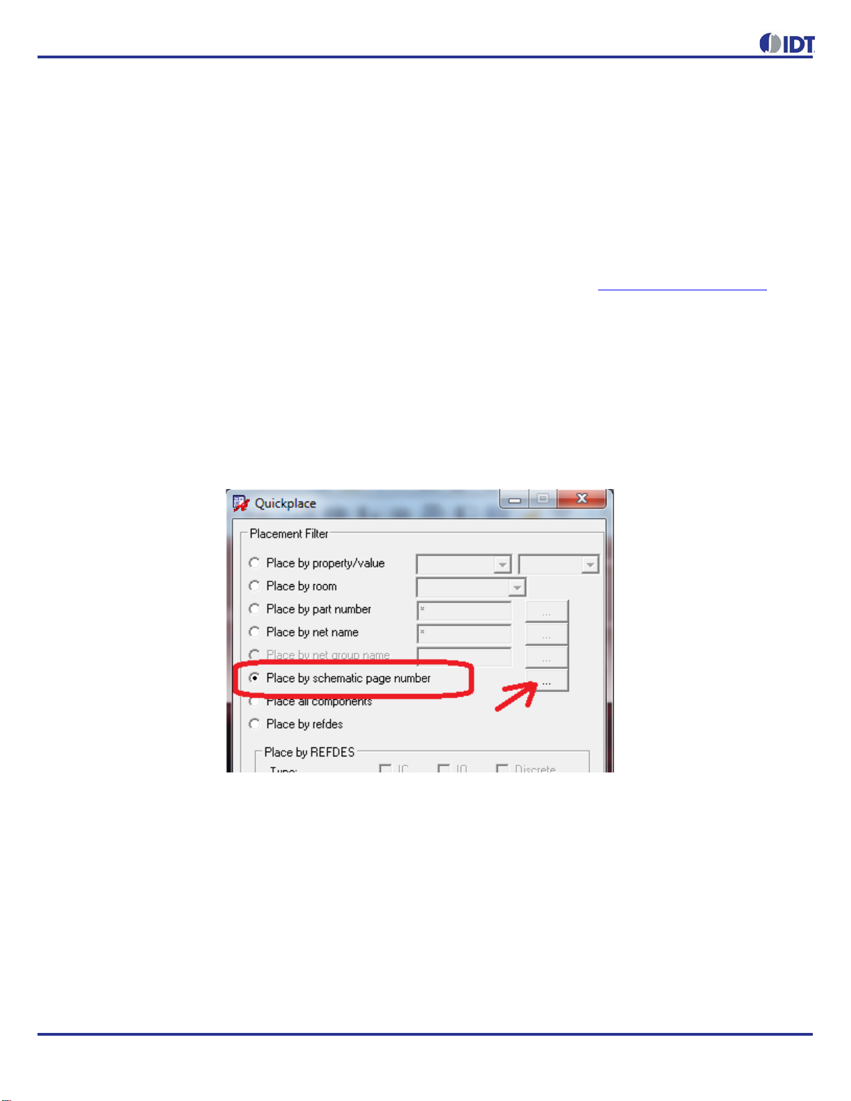
4. Open the PCB design file (.brd) and click on the menu Place→Quickplace…
a. Select Place by Page Number and select the page the P9038 circuitry resides on.
Figure 1. Cadence Quickplace Option Box used for Placing the IDT Layout Module by Page Number
b. Click Place. Click Ok.
5. Select the parts that were placed from the schematic that matches the schematic used from the P9038-R-EVK.
a. In the Find Filter, select Symbols, then left click and drag to highlight all of the components that were just placed.
b. Right click on any of the highlighted parts and select “Place Replicate Apply→Browse…”
c. Select the P9038-R-EVK.mdd file and select Ok.
d. Components should be matched. If unmatched, manually identify and match component reference designators
based on schematic location.
6. Enter the coordinates (x,y location) in the command window where the P9038 circuit should be placed.

08/23/15 3 P9038 LAYOUT GUIDE
AN-894
Connecting a Power Source
The USB input connector accepts micro-USB cables type A or B. If a new design does not need this connector, simply extend
the VIN power trace and GND as needed to the location the new power connector will be placed at. If moving the power
connector is necessary, it is suggested to keep a solid GND plane leading to the new connector location and route VIN at a width
that is at least 100 mils wide as space permits.
Connecting Inputs / Outputs
All input and outputs on the reference board have been placed near the edges of the reference layout such that they can be
easily connected to other parts of the system board. After placing the module in the specific design, use the labeled vias as
connection points for new traces on either the top or bottom layer.
Manufacturing Notes
PCB should be made with a minimum of 1oz copper foil weight per square foot or heavier.
Additional Resources
All support files and collateral for the P9038-R-EVK reference board can be found at http://www.idt.com/P9038-R-EVK. Files
include: schematics, layout files, datasheets, user guides, etc.
P9038 LAYOUT GUIDE 4 08/23/15
AN-894
Custom Layout Guidelines
The P9038 wireless power transmitter is an integrated device consisting of a high power full-bridge inverter designed to drive
wireless LC resonance circuits and transmit power to WPC complaint wireless receivers. In addition to wireless power transfer,
there are noise sensitive circuits, General Purpose I/O's (GPIO's) and two low power linear regulators. When designing the
printed circuit board (PCB) there are multiple considerations and often some trade-offs associated with managing the critical
current paths. In order to optimize the design, components should be placed based on circuit function to guarantee best
performance when the schematic is implemented into a PCB design. Furthermore, the thermal management of the application
is important to the product's performance and should be optimized during PCB design. By following the guidelines set forth in
this document, efficient operation will be obtained for each circuit function.
Layout Priority Checklist
1. Place the Input capacitors and use short, wide connections from IN to PGND (target < 250mils long, > 50 mils wide).
2. Route SW1 and SW2 wide and short (use 6 – 10 vias for layer transitions) (target < 250mils long, > 50 mils wide).
3. Use wide planes (up to 2A) to route from the power connector to the RSENSE & IN and PGND connections.
4. Use sense (Kelvin) connections to connect to the current sense resistor RSENSE. See Figure 9.
5. Create wide continuous connections to the EPAD on bottom or internal PCB layer(s) (at least two 200 to 400 mil wide
channels should be directly connected to the EPAD and uninterrupted by traces for at least 1" leading away from the
IC). Use 25 thermal vias in the EPAD.
6. Place LDO capacitors as close as possible to the P9038.
7. Place Vsns Diode near LC and use 10 mils+ air gap separation from the cathode to the first filter resistor.
8. Place HPF capacitor near the P9038 and shield from switching side with shield resistor.
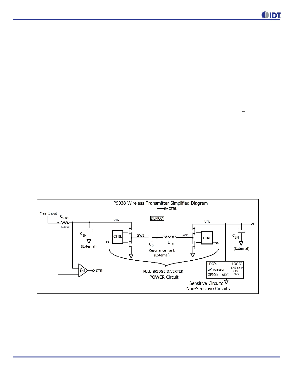
Figure 2. P9038 Simplified Diagram
08/23/15 5 P9038 LAYOUT GUIDE
AN-894
Power Circuits
The integrated Full-Bridge Inverter and the resonance tank are the primary power circuits. Secondary power circuits are the
LDO5V and LDO2P5V voltage regulators. After the connection points for the transmitter coil (LTX) are chosen, the P9038 should
be placed as close to the center of the PCB as possible with SW1 and SW2 pins facing the LC resonance tank. Components
should be placed in the following order of priority:
1. Input capacitors (CIN)
2. BST1, BST2 capacitors
3. Resonance tank (CP and LTX)
4. Zero Voltage Switching (ZVS) capacitors and tuning resistors
5. LDO capacitors
6. Current Sense Resistor (RSENSE)
7. Optional USB input transistor (USB FET, see Application Note AN-867 P9038 OVP and In-Rush Current Limiting
Options for additional details)
8. Current sense filter components
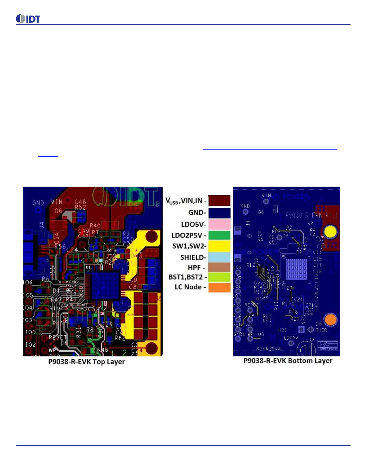
Figure 3. P9038 Physical Layout from REFERENCE PCB (2 layer PCB), Main Power Sensitive Circuits
Figure 3 demonstrates the key nodes and layout recommendations for a 2-layer PCB. Important concepts include CIN direct
routing to IN and PGND pins and wide connections (>=60mils) for VIN. SWx nodes are routed on P9038 side of the PCB and
can easily be extended directly out for PCBs that have more distance to the edge of the board. LDO5V and LDO2P5V capacitors
are located very close to the IC with direct GND return to the EPAD. The EPAD has 25 thermal vias. Traces located on the bottom
layer have been placed as far as possible from the EPAD to create heat flow 'channels' (see the top left and lower regions
surrounding the EPAD on the bottom layer). Solid and continuous GND planes in direct contact with the EPAD will result in lower
operating temperatures and higher efficiency.
P9038 LAYOUT GUIDE 6 08/23/15
AN-894
BST1/2 connections are routed on the top layer and wrap around the PGND connections which each have multiple vias for the
layer transition. Finally, the GND plane on the right side of the slot is adequately wide (similar width to VIN) in order to carry the
RMS input current back to the power supply with minimal voltage drop along its length.
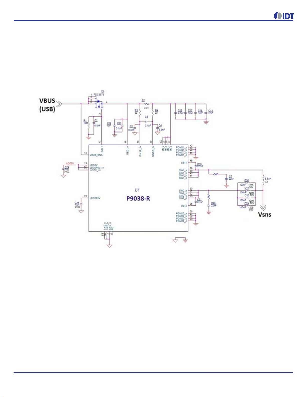
Figure 4. P9038 Full-Bridge Inverter, Current Sense Resistor, and Resonance Tank Schematic.
Note: not all pins are shown in the figure, refer to the P9038 datasheet Pin Description for the complete list of pins and
recommended connections)

08/23/15 7 P9038 LAYOUT GUIDE
AN-894
Figure 5. P9038 2-Layer Layout Main Input Power Example for Routing VIN on Top Layer to Input Capacitors
Input Capacitors
The input capacitors are labeled C13, C15, C17, and C18. Due to the high currents they supply to power the LC resonance tank
and the relatively fast slew rates at the SW1 and SW2 nodes, the connections to the input capacitors must be short and wide (at
least as wide as the four adjacent VIN/SW1/SW2 pins). The ideal placement of the input capacitors is to have them as close as
possible to the P9038 device and symmetrically placed so that the wiring and connections are matched relative to the IN_x pins
(QFN pins 34, 35, 36, 37) and the PGND1 & PGND2 pins (QFN pins 42, 43, 44, 45 & 26, 27, 28, 29). Capacitors with Class II
dielectrics (such as X5R) are required and the effective capacitance should be greater than 10µF at 5VDC bias (see DC Bias
curve of capacitor under consideration). For designs that require less than 2.5W maximum power delivering, the effective
capacitance may be reduced to 6µF at 5VDC. To avoid uncertainty in component selection, it is recommended to use the
components listed in the reference board bill-of-materials.
P9038 LAYOUT GUIDE 8 08/23/15
AN-894
Figure 6. P9038 2-Layer Layout Critical VIN to SW1/SW2 Current Paths from Input Capacitors
It should be noted that the 0.1µF capacitor C18 is located the closest to the P9038 device because the lower capacitance and
ESL of the smaller package allow it to filter higher frequencies more effectively than physically larger components. Since these
are the highest priority signals to filter, it is imperative that the impedance from this component to IN and PGND is minimized.
Next, the three bulk capacitors C13, C15, and C17 are placed next to C18 and kept close to the device as well. The purpose of
this placement orientation is to stabilize the input during switching and to minimize the loop area of the current paths (green
arrows in Figure 6). Minimizing trace lengths will promote lower lead inductance which will result in less GND bounce induced
by the switching voltages and currents during operation. If the PGND/IN/SW connections change layers, each transition should
be made using at least 5 – 8 vias.
08/23/15 9 P9038 LAYOUT GUIDE
AN-894
Figure 7. P9038 Recommended Placement and Top Layer Routing of Full-Bridge Inverter and Resonance
Tank with DC (+ripple(GND Bounce)) Current Path Shown
Inspection of Figure 7 shows how the main power input power rail is routed on the P9038-R-EVK. It is recommended to keep
the SW1 and SW2 signals on the same physical side of the PCB as the P9038 and make VIN switch layers since the SW1/2
signals are AC and more sensitive to vias and layer transfers than the relatively stable (DC + ripple) VIN current.
The connections from the IN caps to IN and PGND pins plus the SW1 and SW2 nodes should be considered capable of radiating
EMI and these should not be allowed to become excessively long (more than 6” (15cm) to either the inductor or resonance
capacitors. If these connections must be longer, it is recommended that they are coupled with a GND plane. The P9038 design
was implemented with optimal EMI performance in mind; therefore, EMI should be acceptable with plenty of margin to pass EMI
compliance testing without the need for additional layout considerations.
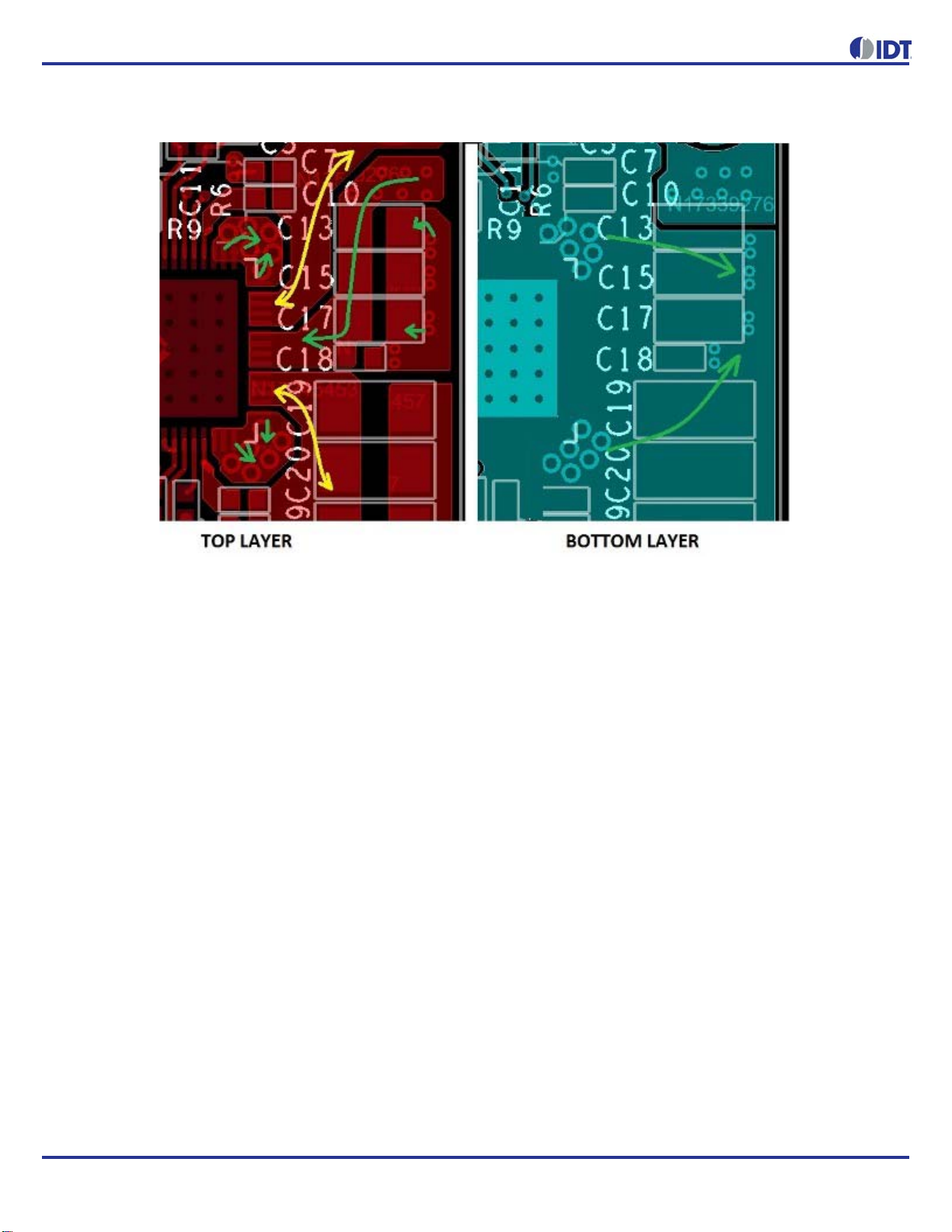
BST and ZVS Capacitors
BST1 capacitor C10 and BST2 capacitor C21 should be placed immediately outside the PGND connections and in direct contact
with the SW1 and SW2 nodes, respectively. The key to properly placing and connecting these capacitors is to keep the
connections from the BSTx pins to the respective switch nodes short and low inductance (15 – 20 mils wide and use 2 vias if
layer transitions are necessary). The BST1 and BST2 capacitors should always be close to the P9038 device.
The ZVS components, C7 for SW1 node and C28 for SW2 node, are ideally placed near the P9038 device and will be routed
around the BST1 & BST2 connections to the respective PGND pins. Maintaining symmetry between the two switching nodes is
recommended to achieve optimal performance.
By inspecting the Figure 8, notice should be taken of the short direct path C10 and C21 have to the SW1 and SW2 nodes and
the way the trace length expands as the connection escapes from the P9038 device. This reduces the inductance of this
connection, which insures full and fast saturation of the gates of the high side switches at the appropriate time for the FETs to
switch. Then the ZVS components are placed and they are routed around the BST1 and BST2 capacitors.

P9038 LAYOUT GUIDE 10 08/23/15
AN-894
Figure 8. Image of BST1, BST2 and ZVS Components for P9038 QFN (VFQFPN) Layout
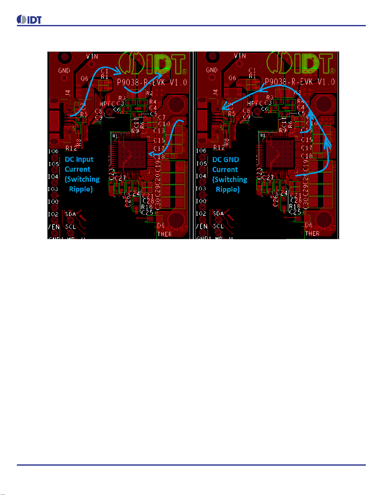
Next, the current sense resistor and the associated filters are crucial for Foreign Object Detection (FOD) accuracy, as they
impact the input power calculations. The P9038 calculates the input power using the voltage on the IN pins and the current
detected as a voltage drop across the sense resistor (R2). Since the signal sensed across this resistor will be 20 mV or below,
signal integrity is important for proper operation. Best practice will follow the guidance in the following image and the length of
these connections will be minimized. The current sense resistor should be placed in close proximity to the P9038 device for best
results. Notice how the voltage drop (+,-) across R2 is Kelvin sensed by filter resistors R3 and R4. This is done to improve
accuracy of the input current measurements needed for FOD. The GND connection for C4 and C3 should be located on the
EPAD GND side of the GND slot.

08/23/15 11 P9038 LAYOUT GUIDE
AN-894
Figure 9. Kelvin Connections to Rsns (R40)
The Input power connections and traces should be routed with adequate width to conduct up to 2 A of DC current with minimal
voltage losses. When using the USB and N-CH FET, a device with an acceptable and minimal RDSON specification should be
selected.
The High Current Power GND will carry the DC input current up to ~ 1.7 A, including the input ripple current at the power transfer
frequency. As a result, it may be prone to varying voltage drops depending on the Rx load and is not recommended to be
common to sensitive GND for DEMOD signals. The Noisy PGND area will have high current switching and rapid voltage changes
induced from the full bridge inverter switching, this area is not suitable to be used for GND reference. The DEMOD circuits GND
connections should be made away from the PGND pins and have a separate current return path to the EPAD from the input
capacitors and the PGND pins.
Next, the LDO input capacitors need to be placed in close proximity to the P9038 device. The P9038 has two Low Drop-Out
(LDO) linear voltage regulators: LDO5V (Pin 19), LDO2P5V (Pin 20). The LDO5V output and LDO2P5V input may share a single
1µF ceramic capacitor for cost reduction or compact designs. Both LDO input and output capacitors should be placed near each
respective LDO pin with the GND plate of the capacitor connected to the EPAD GND area of the PCB. While the LDO's are
technically power circuits, they are sensitive to noise and should not be placed far from the P9038 device to promote stable and
reliable operation.
EPAD
The use of a grid of 25 thermal vias placed inside the E-PAD of the P9038 device is recommended. Using thermal vias and
having one or more GND planes in direct contact is crucial for optimal thermal performance. Typical thermal via diameter is
0.3mm and spacing should be 1mm pitch. The land pattern drawing can be found in the product datasheet.
P9038 LAYOUT GUIDE 12 08/23/15
AN-894
Noise-sensitive Circuits
The sensitive circuits refer to noise sensitive circuits that should be referenced to GND on the side of the P9038 that is furthest
from the PGND pins and input capacitors ("Quiet GND" side). They include the Input current sense filters (previously discussed),
the ISNS_AVG pin (pin 48 for the QFN) connection to capacitor (C47), the LDO pins and filter capacitors, VSNS_AVG (Pin24)
plus capacitor C51, REFGND (pin 17) and the DEMOD WPC communication filters. The most important guidance with respect
to layout for all of these sensitive circuits is to tie them to GND on the opposite side of the IC from the PGND pins.
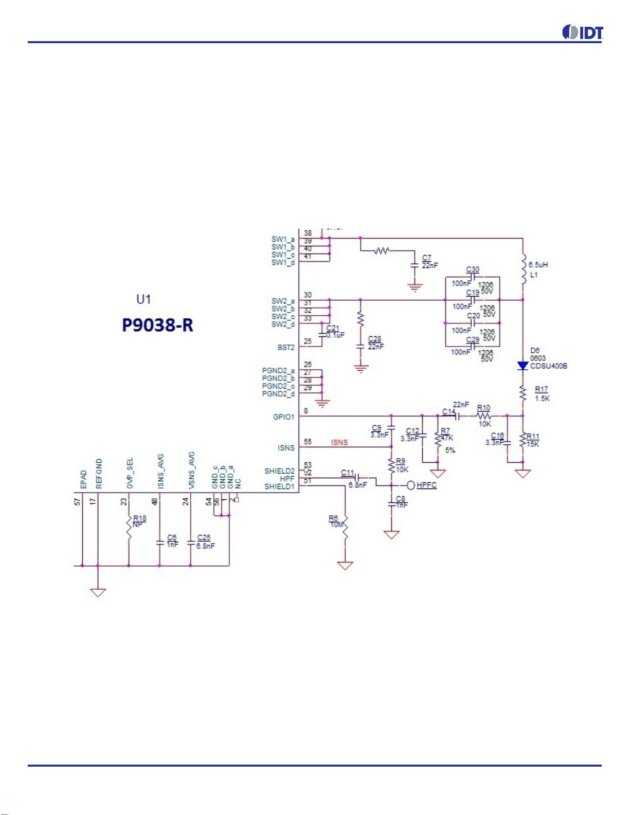
Figure 10.P9038 DEMOD Communication Filters and Accompanying Components
Note: not all pins are shown in the figure)
Figure 10 shows all of the components considered part of the DEMOD filters connected to the Tx coil, along with a few other
sensitive components and pins. The optimal layout will have the anode of diode D6 placed close to the LC resonance node, and
the remaining DEMOD filter components adjacent to the P9038 device in the 'Quiet' GND area. The connection from the cathode
of D6 to R17 is subject to periodic high voltage surges near 50V-peak and should be given at least 10 mils of clearance from any
other net or connection. Resistors R6 and the connections to SHEILD1 (pin 51) should be kept in close proximity and use the
same GND connection as the point where C8 is merged with the rest of the GND circuits (in the 'Quiet' GND area). The input
connection from C11 to the HPF (pin 52) is high impedance and is the most noise sensitive pin on the device. Extra care must
be taken to route connections from HPF to C11 & C8 / R9. ISNS to C9 trace lengths should be minimized and avoid routing near
PGND and VIN or SW1 and SW2 switching signals that exist on the PCB.

08/23/15 13 P9038 LAYOUT GUIDE
AN-894
Figure 11. Sensitive DEMOD, Rsns Filter, LDO GND Located on opposite side of the P9038 from the PGND
pins. Provide GND connection directly to EPAD for these GNDs.
The current sense connections from R2 to R3 and R4 are done in a Kelvin manner, directly to the pins of R2. This is done to get
the most accurate voltage drop across the sense resistor prior to filtering and amplification by the internal differential amplifier
used to help calculate input power for FOD.
Non-sensitive Circuits
The remaining components and pins that have not been mentioned are regarded as non-sensitive circuits. The placement and
routing of these nodes is not considered critical to performance or functionality, and so they simply need to be present and
properly connected. In most cases, 6 mil wide traces and any method of connectivity will suffice to complete the circuit.
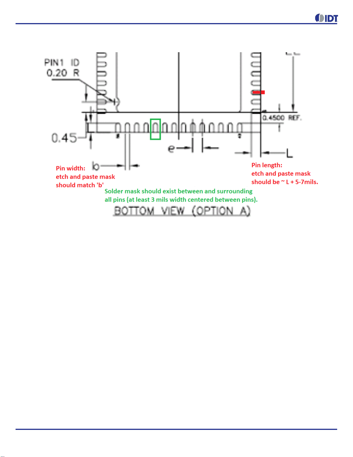
PCB Footprint Design
PCB Footprint can have a substantial impact on reliability and production yield. In order to avoid placement and soldering issues
during assembly and product deployment, it is recommended to allow sufficient copper landing pads to be exposed, utilize
soldermask, and apply a proper amount of solder paste to the IC. Furthermore, PCB cleaning is highly recommended after the
reflow process is completed.
The P9038 datasheet should be referenced during footprint design, and the following image provides some additional landing
pad allowance and soldermasking recommendations. The exposed pin (etch) used to solder the IC to the PCB must be at least
as large as the physical pin of the package. It is highly recommended to add some additional length (L) to each pin to promote
proper soldering. It is imperative to include soldermask around each pin in order to eliminate potential solder shorts during
assembly and reflow. It is also not suggested to pour continuous copper planes in the pin area. Instead, use a small trace to
connect pins to the planes.
P9038 LAYOUT GUIDE 14 08/23/15
AN-894
Figure 12.P9038 PCB Footprint Design Guidance
Thermal Performance
PCB design can have a substantial impact on operating temperature and efficiency. In order to allow the P9038 to operate at the
lowest possible temperature, the EPAD must be connected directly to a GND plane and traces on the bottom layer should be
kept as short as possible and be routed as far away from the EPAD as possible to promote heat flow paths and heat dissipation.
Traces, vias, or voids will block heat flow and result in increased operating temperatures. The 2.1" x 1.134" reference board, as
designed, operates near 49°C when delivering 5 W.

08/23/15 15 P9038 LAYOUT GUIDE
AN-894
Figure 13.P9038-R-EVK Bottom Layer Heat Flow Paths and Thermal Image when delivering 5 W to the
P9025AC-R-EVK (board is 2.1" x 1.134" in area near the application circuitry). Metallic Surfaces Appear
Cooler than they are due to their Emissivity.
Figure 14.P9038-R-EVK Top Layer Thermal Image when delivering 5W to the P9025AC-R-EVK (board is 2.1"
x 1.134" in area)

DISCLAIMER Integrated Device Technology, Inc. (IDT) and its subsidiaries reserve the right to modify the products and/or specifications described herein at any time and at IDT’s sole discretion. All information in
this document, including descriptions of product features and performance, is subject to change without notice. Performance specifications and the operating parameters of the described products are determined
in the independent state and are not guaranteed to perform the same way when installed in customer products. The information contained herein is provided without representation or warranty of any kind, whether
express or implied, including, but not limited to, the suitability of IDT’s products for any particular purpose, an implied warranty of merchantability, or non-infringement of the intellectual property rights of others. This
document is presented only as a guide and does not convey any license under intellectual property rights of IDT or any third parties.
IDT’s products are not intended for use in applications involving extreme environmental conditions or in life support systems or similar devices where the failure or malfunction of an IDT product can be reasonably
expected to significantly affect the health or safety of users. Anyone using an IDT product in such a manner does so at their own risk, absent an express, written agreement by IDT.
Integrated Device Technology, IDT and the IDT logo are registered trademarks of IDT. Product specification subject to change without notice. Other trademarks and service marks used herein, including protected
names, logos and designs, are the property of IDT or their respective third party owners.
Copyright ©2015 Integrated Device Technology, Inc.. All rights reserved.
Corporate Headquarters
6024 Silver Creek Valley Road
San Jose, CA 95138 USA
Sales
1-800-345-7015 or 408-284-8200
Fax: 408-284-2775
www.IDT.com
Tech Support
www.idt.com/support/technical-support
This manual suits for next models
1
Table of contents


