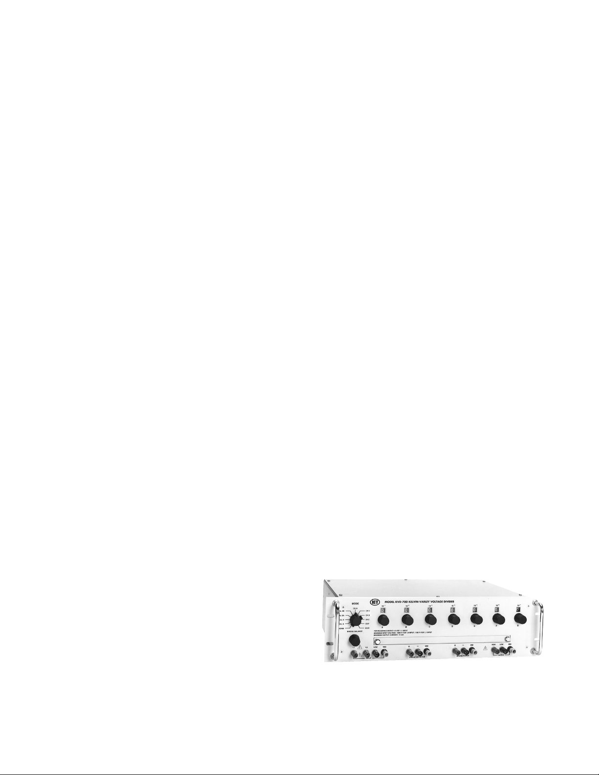
IET Labs KVD-700 Series User manual

♦PRECISION INSTRUMENTS FOR TEST AND MEASUREMENT ♦
TEL: (516) 334-5959 • (800) 899-8438 • FAX: (516) 334-5988
www.ietlabs.com
534 Main Street, Westbury, NY 11590
IET LABS, INC.
KVD-700 SERIES
KELVIN-VARLEY
VOLTAGE DIVIDER
Operation Manual
Copyright 2007 IET Labs, Inc.
Effectivity: Serial Numbers prefixed G
KVD-700im/08-07

♦PRECISION INSTRUMENTS FOR TEST AND MEASUREMENT ♦
TEL: (516) 334-5959 • (800) 899-8438 • FAX: (516) 334-5988
www.ietlabs.com
534 Main Street, Westbury, NY 11590
IET LABS, INC.

iii
WARRANTY
We warrant that this product is free from defects in material and workmanship and, when properly used, will
perform in accordance with applicable IET specifications. If within one year after original shipment, it is found
not to meet this standard, it will be repaired or, at the option of IET, replaced at no charge when returned to IET.
Changes in this product not approved by IET or application of voltages or currents greater than those allowed by
the specifications shall void this warranty. IET shall not be liable for any indirect, special, or consequential
damages, even if notice has been given to the possibility of such damages.
THIS WARRANTY IS IN LIEU OF ALL OTHER WARRANTIES, EXPRESSED OR IMPLIED, INCLUD-
ING BUT NOT LIMITED TO, ANY IMPLIED WARRANTY OF MERCHANTIBILITY OR FITNESS FOR
ANY PARTICULAR PURPOSE.

vii
WARNING
OBSERVE ALL SAFETY RULES
WHEN WORKING WITH HIGH VOLTAGES OR LINE VOLTAGES.
Dangerous voltages may be present inside this instrument. Do not open the case
Refer servicing to qulified personnel
HIGH VOLTAGES MAY BE PRESENT AT THE TERMINALS OF THIS INSTRUMENT
WHENEVER HAZARDOUS VOLTAGES (> 45 V) ARE USED, TAKE ALL MEASURES TO
AVOID ACCIDENTAL CONTACT WITH ANY LIVE COMPONENTS.
USE MAXIMUM INSULATION AND MINIMIZE THE USE OF BARE
CONDUCTORS WHEN USING THIS INSTRUMENT.
Use extreme caution when working with bare conductors or bus bars.
WHEN WORKING WITH HIGH VOLTAGES, POST WARNING SIGNS AND
KEEP UNREQUIRED PERSONNEL SAFELY AWAY.
CAUTION
DO NOT APPLY ANY VOLTAGES OR CURRENTS TO THE TERMINALS OF THIS
INSTRUMENT IN EXCESS OF THE MAXIMUM LIMITS INDICATED ON
THE FRONT PANEL OR THE OPERATING GUIDE LABEL.

Contents
WARRANTY ...........................................................................................iii
WARNING ............................................................................................... v
CAUTION................................................................................................ v
Chapter 1
INTRODUCTION .......................................................................... 1
1.1 General Description ............................................................... 1
1.2 Circuit Description ................................................................. 2
1.2.1 Model ............................................................................ 2
1.2.2 Theory of Operation ...................................................... 2
Chapter 2
SPECIFICATIONS ......................................................................... 5
Chapter 3
INSTALLATION ............................................................................ 7
3.1 Initial Inspection ..................................................................... 7
3.2 Installation .............................................................................. 7
3.3 Repackaging for Shipment ..................................................... 7
3.4 Storage ................................................................................... 7
Chapter 4
OPERATION ................................................................................... 8
4.1 Initial Inspection and Setup .................................................... 8
4.2 Power Considerations ............................................................ 8
4.3 Loading Errors ....................................................................... 8
4.4 Switch Conditioning ............................................................... 9
4.5 Operation and Controls .......................................................... 9
4.6 Representative Bridge Applications of the KVD-700 ......... 10
Chapter 5
SELF-CALIBRATION ................................................................ 11
5.1 Introduction .......................................................................... 11
5.2 End Errors ............................................................................ 11
5.3 Self-Calibration Setup .......................................................... 13
5.4 Self-Calibration Procedure .................................................. 13
5.4.1 First Decade ................................................................ 13
5.4.2 Second Decade ........................................................... 14
5.4.3 Shunt Resistors ............................................................ 14
Chapter 6
VERIFICATION, CALIBRATION AND MAINTENANCE 15
6.1 Preventive Maintenance ...................................................... 15
6.2 Overview of Verification of Performance and Calibration .. 15
6.3 Required Test Equipment .................................................... 15
6.4 Verification of Leakage Resistance ..................................... 15
6.5 Verification of Absolute Linearity of First Decade .............. 16
6.6 Verification of Decades (B through G) Linearity ................ 19

6.6.1 Decade B .................................................................... 19
6.6.2 Decade C .................................................................... 21
6.6.3 Decade D .................................................................... 21
6.6.4 Decade E .................................................................... 22
6.6.5 Decade F ..................................................................... 22
6.6.6 Decade G .................................................................... 22
6.7 Calibration ............................................................................ 23
6.7.1 Calibration of C Decade.............................................. 23
6.8 Bridge Calibration ................................................................ 24
6.8.1 Bridge C Arm Calibration ............................................ 24
6.8.2 Bridge A-B Arm Calibration........................................ 24
6.9 Parts Diagrams and Schematic ........................................... 24
Appendix A
BIBLIOGRAPHY ......................................................................... 28
Figures
Figure 1.1. Model KVD-700 Kelvin-Varley Voltage Divider .............................................................................. 1
Figure 1.2. Digital Potentiometer Model for a Kelvin-Varley Voltage Divider .................................................... 2
Figure 1.3. Thevenin Equivalent Circuit of a Kelvin-Varley Voltage Divider ...................................................... 2
Figure 1.4. Approximate Value of Output Resistance as a Function of Dial Setting (S) ..................................... 3
Figure 1.5. Schematic Diagram of KVD-700 Kelvin-Varley Voltage Divider Circuit ......................................... 4
Figure 2.1. Typical OPERATING GUIDE Affixed to Unit ................................................................................. 6
Figure 4.1. Front Panel of KVD-700 ................................................................................................................... 9
Figure 5.2. Setup Diagram for Measurement of Zero End Correction Relative to Output Common ................ 12
Figure 5.3. Setup Diagram for Measurement of Full Scale Correction ............................................................. 12
Figure 5.1. Setup Diagram for Measurement of Zero End Correction Relative to Input Common .................. 12
Figure 5.4. Setup for Self-Calibration ................................................................................................................ 13
Figure 6.2. Setup for Leakage Resistance Test ................................................................................................. 16
Figure 6.1 Required Equipment for Verification ................................................................................................ 16
Figure 6.3. Conceptual Representation of Linearity Verification Test ............................................................... 17
Figure 6.4. Setup for Linearity Verification Test for First Decade .................................................................... 18
Figure 6.5. Setup for Linearity Verification Test for Decades B through G ...................................................... 20
Figure 6.6. Bottom View of Calibration Board and Location of C Decade Trimmers (Legend is printed on
opposite side of board; is shown here for clarity) ........................................................................... 25
Figure 6.7. Layout of Internal Bridge Calibration Board and Location of Trimmers ........................................ 25
Figure 6.9. Parts Location: Top View of Unit .................................................................................................... 26
Figure 6.8. Parts Location: Front Panel ............................................................................................................. 26
Figure 6.10. Parts Location: Calibration PC Board ........................................................................................... 27

1
Introduction
KVD-700
Chapter 1
INTRODUCTION
1.1 General Description
The KVD-700 (Figure 1.1) is a calibration grade volt-
age divider employing the Kelvin-Varley circuit. It is
a highly accurate, stable, and linear primary ratio stan-
dard suitable for use in many applications requiring
known voltage or current ratios. In particular, the
KVD-700 is especially appropriate for use in bridge
circuits, providing two legs of a bridge with a very
well known ratio.
The KVD-700 has a resolution of 0.1 ppm and an
absolute linearity of 0.1 ppm. It has a 1.0 input and a
1.1 input to allow over-ranging. Temperature coeffi-
cient of linearity is 0.1 ppm/ºC, and power coefficient
of linearity is 0.2 ppm/W.
The KVD-700 incorporates a number of advanced
features making for convenience and high perfor-
mance. These include: self-calibration capability; state
of the art nominally “zero tempco bulk metal foil re-
sistors”; Kel-F mounted low-emf tellurium copper
binding posts; sealed internal calibration potentiom-
eters; and a convenient operating guide attached to
the unit.
The KVD-700 features a built-in Wheatstone bridge
self-calibration circuit so that the unit may be cali-
brated with a minimum of external instruments and
without requiring another voltage divider.
The KVD-700 employs precision resistors which have
been aged, temperature and power cycled to maxi-
mize long-term stability, and matched to minimize tem-
perature and power coefficients effects. The most
significant decade is sealed in an oil bath to minimize
temperature coefficient effects.
The switches used have gold plated solid silver alloy
contacts for long life, minimum contact resistance,
and no tarnishing. Gold also allows the use with low
level signals. The switches have multiple wiper con-
tacts to provide stable low contact resistance. The
main switches are sealed.
High quality gold plated tellurium-copper binding posts
serve to minimize the thermal emf effects which would
artificially reflect a change in dc resistance measure-
ments. They are mounted to the case on special Kel-
F washers to insure low leakage. All other conduc-
tors within the instrument, as well as the solder em-
ployed, contain no metals or junctions that could con-
tribute to thermal emf problems.
The front panel is clearly labelled showing step size
for each decade. Maximum voltage and current lim-
its are indicated as well. The unit may be mounted in
a standard 19-inch rack.
Applications include linearity determination, the mea-
surement of voltage and resistance, and the calibra-
tion of other dividers, potentiometers or similar de-
vices involving both voltage and current.
Figure 1.1. Model KVD-700 Kelvin-Varley Voltage
Divider
08-07

2Introduction
KVD-700
1.2 Circuit Description
1.2.1 Model
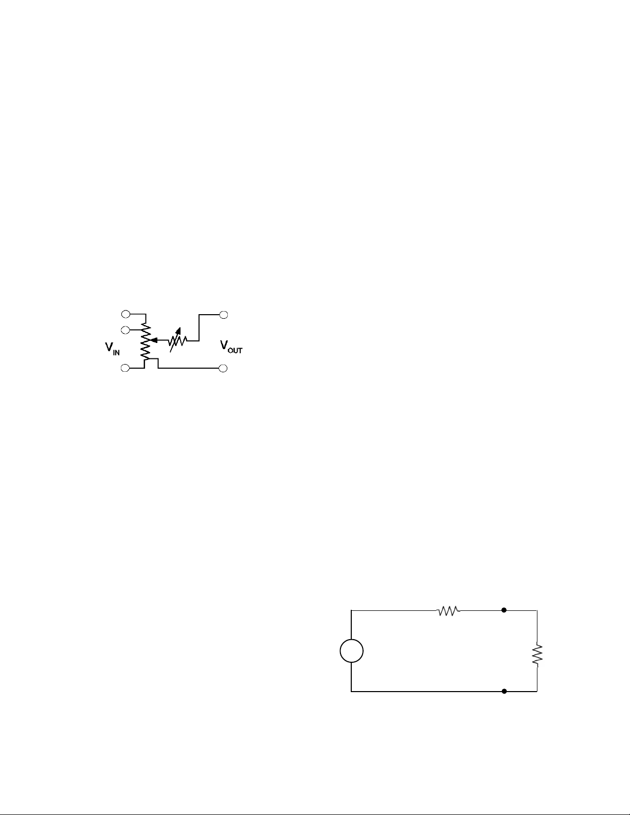
AKelvin-Varley voltage divider may be thought of as
being equivalent to a digital potentiometer, except that
it has an additional, but variable resistance in series
with the wiper arm. Such a circuit model of the KVD-
700 may be seen in Figure 1.2. In the case of the
KVD-700, the resistance between the input termi-
nals 1 and LOW is 100 kΩ.
An actual digital potentiometer uses decades of re-
sistor steps each decreasing by factor of ten. The
problem with such a digital potentiometer, however,
is that its resolution becomes limited by the value of
ever smaller resistors. They become difficult to imple-
ment as the contact resistance of switches and con-
nections become significant. AKelvin-Varley circuit
overcomes this problem with its special design, de-
scribed later.
Another way to model the KVD-700 is with the
Thevenin equivalent circuit shown in Figure 1.3, where
S is the dial setting. Note that if the output is being
fed into a very high impedance, then the output im-
pedance RO, may be ignored. In general, however,
the effect of load impedance, RLmust be taken into
consideration, as will be discussed below. The ap-
proximate value of ROis shown in Figure 1.4. It may
be seen that the output impedance is maximum at
about the dial setting of 0.5 and drops to zero at both
ends, 1.0 and 0. It is the value of ROwhich will influ-
ence the effect of loading.
Note, however, that in general bridge applications,
nominally zero current flows out of the divider as the
bridge comes into balance, and therefore the divider
effectively “sees” an infinite impedance, and the ef-
fect due to ROmay be safely ignored.
1.2.2 Theory of Operation
The actual circuit diagram of the KVD-700 is shown
in Figure 1.5. This circuit is capable of dividing the
input into 107parts, i.e. 0.1 ppm. It consists of seven
decades, each of which divides its input voltage into
10 equal parts.
The implementation of this division may be seen as
follows: The input voltage across each decade is di-
vided by 10 equal resistances. Placing the resistance
of the succeeding decade in parallel with a portion of
the upstream decade reduces the effective resistance
of that portion. In particular, examine the figure and
note that first decade has 11 - not 10 - resistors (ig-
noring the 1.1 input resistor). The divider wipers from
the second decade encompass two resistors totaling
20 kΩ. This 20 kΩis shunted by 20 kΩ, the effective
total resistance of the second decade with all the
shunting in parallel with it, resulting in a total effec-
tive resistance of 10 kΩfor that step.
The 11 steps become equivalent to 10 steps of 10 kΩ
each, and in this way all the steps are kept equal.
1.1
1.0
LOW
HIGH
LOW
Figure 1.2. Digital Potentiometer Model for a Kelvin-
VarleyVoltage Divider
INPUT OUTPUT
SVIN V
OUT RL
RO
Figure 1.3.Thevenin Equivalent Circuit of a Kelvin-
VarleyVoltage Divider
R0

3
Introduction
KVD-700
Note that the last decade uses only one switch wiper
and can therefore span positions 0-10. With all sig-
nificant decades set to 9, and the last one set to 10,
the output is 1.0 or equal to the input.
At the low or zero end, a small series resistance is
added between the OUTPUT LOW terminal, the
lower end of the divider string, and the INPUT LOW
terminal to compensate for contact and wiring resis-
tance, thus bringing the voltage at the OUTPUT
LOW terminal equal to the voltage at the OUTPUT
HIGH terminal for all switches set to 0. This pro-
vides improved performance for low voltage outputs.
Each step of the second decade is also 10 kΩ. The
20 kΩof that decade, spanned by the switch con-
tacts, are shunted by the 20 kΩeffective resistance
of the third decade. Similarly 8 kΩof the third de-
cade are shunted by the 8 kΩtotal resistance of the
fourth decade.
Note that this pattern reduces the resistor value until
an optimal value of 1 kΩis reached and repeated.
This allows the use of a resistance high enough to
avoid contact resistance problems.
RATIO DIAL SETTINGS (S)
Note:The value of the output resistance is a“smoothed” approximation.
The actual resistance “oscillates” around this value as lower decades are varied.
Figure 1.4. Approximate Value of Output Resistance as a Function of Dial Setting (S)

4Introduction
KVD-700
Figure 1.5. Schematic Diagram of KVD-700 Kelvin-Varley Voltage Divider Circuit

5
Specifications
KVD-700
Chapter 2
SPECIFICATIONS
Temperature Coefficient of Input Resistance:
±1.0 ppm/ºC.
Maximum Input Power:
10 W at 1.0 INPUT; 11 W at 1.1 INPUT.
Maximum Output Resistance:
66 kΩ, determined by shorting across the input
and measuring the resistance across the out-
put terminals. See Figure 1.4.
Thermal Voltages:
<0.5 µV at the output terminals.
End Errors:
Zero error at OUTPUT LOW terminal <±0.004
ppm of input;
Zero error at INPUT LOW terminal <±0.05 ppm
of input;
Full scale error at OUTPUT HIGH terminal
<±0.05 ppm of input.
Terminals:
High-quality low-thermal-emf, gold-plated, tellu-
rium-copper binding posts; standard 0.75”
spacing; additional binding posts are con-
nected to the case for shielding. Terminals
are insulated from the case by non-moisture-
absorbing Kel-F spacers.
Operating Conditions:
0ºC to 50ºC; 35% RH to 55% RH; for operating
conditions below 15ºC and above 35ºC, lin-
earity must be derated 0.1 ppm/ºC from the
temperature of calibration.
Storage Temperature:
-34ºC to 70ºC.
Dimensions:
5.25" high 19” rack panel;
Panel: 48.3 cm W x 13.2 cm H (19.0" x 5.20")
Behind panel: 42.7 cm W x 12.4 cm H x 31.5 cm
D (16.8" x 5.2" x 12.4");
In front of panel 3.8 cm (1.5").
Weight:
8 kg (18 lb)
For convenience to the user, the pertinent specifica-
tions are given in an OPERATING GUIDE, typi-
cally shown in Figure 2.1, affixed to the case of the
instrument.
Ratio Range:
0 to 1.0 of input at 1.0 INPUT; 0 to 1.1 at 1.1
INPUT.
Resolution:
0.1 ppm with 7 decades.
Absolute Linearity:
At 23ºC, at low power; defined relative to zero
and full scale outputs, at the output termi-
nals. Quantitatively it is [Vout/ Vin] - S, where
S is the dial setting.
±0.1 ppm for S = 0.1 to 1.1.
±0.1 (10S)1/3 ppm for S = 0 to 0. 1.
Short Term Linearity Stability:
When maintained under standard laboratory con-
ditions of ±lºC and applied voltage of
<100 V, linearity shall have a stability of ±0.01
ppm per day, and ±0.1 ppm per month.
Long Term Linearity Stability:
± 1.0 ppm/year for S = 0.1 to 1. 1.
± 1.0(10S)2/3 ppm/year for S = 0 to 0.1.
Self-calibration restores linearity to 0.1 ppm.
Temperature Coefficient of Linearity:
±0.1 ppm/ºC for S = 0.1 to 1.1.
±0.1(10S)2/3 ppm/ºC for S = 0 to 0.1.
Power Coefficient of Linearity:
±0.2 ppm/W for S = 0.1 to 1.1.
±0.2(10S)2ppm/Ωfor S = 0 to 0.1.
Maximum Input Voltage:
1000 V at 1.0 INPUT; 1100 V at 1.1 INPUT.
Maximum Output Current:
11 mA.
Breakdown Voltage:
2500 V to case at sea level; 2000 V to case at
10,000 feet above sea level.
Input Resistance:
100 kΩ±50 ppm at 1.0 INPUT; 110 kΩ±50
ppm at 1.1 INPUT.

6Specifications
KVD-700
Figure 2.1.Typical OPERATING GUIDE Affixed to Unit

7
KVD-700
Installation
Chapter 3
3.3 Repackaging for Shipment
If the instrument is to be returned to IET Labs, con-
tact the Service Department at the number or ad-
dress, shown on the front cover of this manual, to
obtain a “Returned Material Authorization” (RMA)
number and any special shipping instructions or as-
sistance. Proceed as follows:
1. Attach a tag to the instrument identifying the
owner and indicate the service or repair to
be accomplished. Include the model num-
ber, the full serial number of the instrument,
the RMA number, and shipping address.
2. Wrap the instrument in heavy paper or plastic.
3. Protect the front panel and any other protru-
sions with cardboard or foam padding.
4. Place instrument in original container or equally
substantial heavy carton.
5. Use packing material around all sides of in-
strument.
6. Seal box with strong tape or strapping.
7. Mark shipping container “DELICATE IN-
STRUMENT,” “FRAGILE,” etc.
3.4 Storage
If this instrument is to be stored for any lengthy pe-
riod of time, it should be sealed in plastic and stored in
a dry location. It should not be subjected to tempera-
ture extremes. Extended exposure to such tempera-
tures can result in an irreversible change in resistance,
and require recalibration.
INSTALLATION
3.1 Initial Inspection
IET instruments receive a careful mechanical and elec-
trical inspection before shipment. Upon receipt, verify
that the contents are intact and as ordered. The in-
strument should then be given a visual and opera-
tional inspection.
If any shipping damage is found, contact the carrier
and IET Labs. If any operational problems are en-
countered, contact IET Labs and refer to the war-
ranty at the beginning of this manual.
Save all original packing material for convenience in
case shipping of the instrument should become nec-
essary.
3.2 Installation
For a rack mounted model, installation on a 19 inch
rack may be made using the slots in the rack mount-
ing ears. A mounting location that does not expose
the unit to excessive heat or temperature variations is
recommended.
For bench models, no installation as such is required,
because this instrument series is not powered. Since
the KVD-700 is a high accuracy instrument, it is rec-
ommended that a bench space be provided that would
not expose it to abuse and keep it protected from tem-
perature extremes and contaminants.

8Operation
KVD-700
Chapter 4
OPERATION
the unit should be allowed to cool for a few hours
before the application of low power.
4.3 Loading Errors
As may be seen from Figure 1.3, the output voltage
of an unloaded Kelvin-Varley divider is given by:
VOUT = SVIN + DEV
where DEV is the fractional linearity deviation. When
a load is applied, the output becomes:
VOUT = SVIN + DEV - RO/RL
where ROis the output resistance which may be de-
termined by shorting the input leads and measuring
across the output leads, or can be approximated by
using Figure 1.4. ROranges from zero to about 66 kΩ.
RLis the load resistance applied at the output.
It may be seen that it is the relative size of the term
RO/RLto the linearity deviation that determines the
Importance of the loading error. In particular, for the
KVD-700, RLmust be greater than 1 TΩ, i.e. 1012,
for the loading effect to be <.03 ppm for the maxi-
mum RO. It will be smaller for lower output resis-
tances at other settings.
Note that even meters having virtually “open circuit”
input impedance, e.g. 10 GΩ, will still have an effect
on linearity of up to many ppm’s, depending on set-
ting S.
A bridge circuit under balanced conditions will effec-
4.1 Initial Inspection and Setup
This instrument was carefully inspected before ship-
ment. It should be in proper electrical and mechani-
cal order upon receipt.
An OPERATING GUIDE, like the typical one
shown in Figure 2.1, is attached to the case of the
instrument to provide ready reference to specifica-
tions.
4.2 Power Considerations
It is possible to damage the KVD-700 by applying
too great a voltage to the input terminals or drawing
more than 11 mA from the output terminals.
The input or output must therefore be limited in some
fashion. A power supply with current limiting may be
used, or current limiting in the form of a resistor or an
11 mA fuse may be inserted in series with the input
and/or output.
Whenever significant power is applied to the KVD-
700, it should be allowed to stabilize for a few min-
utes as settings are changed. As may be seen from
figure 1.5, if 10 W were applied across the most sig-
nificant decade resistor string, 1 W would be dissi-
pated across each 10 kW resistor, but only 0.25 W
would be dissipated across the two resistors shunted
between the wiper arms. This causes differential
heating, and the drift must be allowed to stabilize. The
oil bath in which the most significant decade is con-
tained serves to more evenly distribute the tempera-
ture variation. After the application of high power,

9
Operation
KVD-700
tively draw no current from the KVD-700 and ap-
proach a true open circuit.
4.4 Switch Conditioning
The main switch wipers employed in this unit are self-
cleaning, and are constructed of solid silver alloy with
solid silver alloy contacts. Whenever left idle, all the
wipers and contacts should still be conditioned or
“rebroken in” to remove any oxide that develops over
time. This is standard metrology practice when high
accuracy is required. This effect is of the order of
less than 1 mΩ, so it may be ignored whenever mea-
surements of that magnitude are not important.
To perform this “breaking in,” simply rotate each
switch seven to ten times in each direction.
4.5 Operation and Controls
Figure 4.1 shows the front panel and the various con-
trols and connection terminals of the KVD-700 di-
vider.
In normal operation, place the MODE switch in the
NORM position. The other positions are for the vari-
ous calibration steps described later.
The input voltage is usually connected to the 1.0 IN-
PUT or if required to the 1.1 INPUT. The latter is
used whenever an “overrange” output greater than
100% of a nominal value is required. Secure con-
nections should be made to the terminals using spade
lugs, banana jacks, or bare wire. Caution should be
exercised since most often such connectors are usu-
ally made of brass which can add thermal emf. Cop-
per or copper alloy connections should be used, or
bare wire which is tinned copper may be employed.
Similar connections are made to the OUTPUT ter-
minals.
Implement any current limiting protection as described
in the power considerations discussion of section 4.2.
Observe all safety precautions if high voltages are
used.
The dials may be set and read directly on the front
panel. Some decades have a CAL and blank posi-
tions to be used only in the calibration mode. The
least significant decade has a 10 setting which can
be use to provide an output of 1.0, i.e. 100% of the
input.
If the KVD-700 is to be used at a temperature con-
siderably different from its latest calibration tempera-
ture or if an extended period of time has passed since
its latest calibration, a self calibration should be per-
formed as described in the Chapter 5.
End errors should be considered in any application.
Either the specified values should be used or the end
errors may measured as described in the Verifica-
tion, Calibration and Maintenance section below.
Figure 4.1. Front Panel of KVD-700
08-07

10 Operation
KVD-700
4.6 Representative Bridge Applications
of the KVD-700
There is a broad spectrum of applications for a Kelvin-
Varley divider, such as calibrating other voltage divid-
ers, measuring unknown voltages, and measuring un-
known resistances. There are a number of sources
for detailed information on these -common and many
other applications. Some are given in Appendix A.
One application, the calibration of a voltage divider is
essentially described in the following chapter on cali-
brating the KVD-700.
Consult IET Labs for additional references and in-
formation.

11
Self-Calibration
KVD-700
Chapter 5
SELF-CALIBRATION
out consideration for end errors. This is done for ex-
ample, when two dividers are compared to each other.
In other applications, this is not practical and the end
error corrections must be applied. Proceed as fol-
lows to determine these corrections:
1. Connect the equipment as shown in Figure 5.1
and set the voltage source to 1000 V. MODE
switch should be at NORM, and all switches
set to 0. In the tests to follow the voltages
measured represent a relation of 10 µV to
.01 ppm. Convert the voltages accordingly.
Set the KVD-700 to zero and measure the
voltage between the OUTPUT HIGH and
the INPUT LOW. This is the zero or low
end correction relative to input common. Con-
firm that it is <±0.05 ppm of input.
2. Change the setup to the configuration of Fig-
ure 5.2. Note the change in the polarity of
the voltage source. MODE switch should
be at NORM, With the KVD-700 still set to
zero, now measure the voltage of the OUT-
PUT HIGH relative to OUTPUT LOW.
This is the zero or low end correction rela-
tive to output common. Confirm that it is
<±0.004 ppm of input.
3. Modify the setup as shown in Figure 5.3. Set
all dials to full scale (999 999 10) and mea-
sure the voltage between the OUTPUT
HIGH and the INPUT HIGH. This is the
full scale correction. Confirm that it is <±0.05
ppm of input.
4. Repeat the above steps for the 1.1 INPUT.
Note that full scale is now 10 99999 10
5.1 Introduction
As may be seen from the schematic of a Kelvin-Var-
ley voltage divider shown in Figure 1.5, the linearity
depends primarily on the equivalence of the resistance
steps.
The self-calibration feature takes advantage of this
fact by incorporating a Wheatstone bridge to make
all the resistance steps equal to one step used as a
reference. Adjustable trimmers in the first three de-
cades allow setting the various resistors and shunts
with respect to the initial reference resistance. This
can compensate for the effects of aging and tem-
perature and results in maintenance of the absolute
linearity to ±0.1 ppm of input.
5.2 End Errors
The absolute linearity deviations specified or verified
in the procedure below are with respect to the output
terminals, i.e. they assume that the settings of 0 and
1.0 are defined as correct. Linearity relative to the
input, i.e. terminal linearity requires the following pro-
cedure. Two end corrections are obtained, one rela-
tive to the input common terminal and the second rela-
tive to the output common terminal. These correc-
tions, as well as the full scale correction, account for
the uncompensated portion of the contact and wiring
resistances.
If a lead compensator were used, as described in the
next chapter, then absolute linearity may be used with-
8-07

12 Self-Calibration
KVD-700
Figure 5.1. Setup Diagram for Measurement of Zero End Correction Relative to Input Common
Figure 5.2. Setup Diagram for Measurement of Zero End Correction Relative to Output Common
Figure 5.3. Setup Diagram for Measurement of Full Scale Correction
8-07

13
Self-Calibration
KVD-700
5.3 Self-Calibration Setup
Refer to Figure 5.4 to set up the KVD-700 for self
calibration. Use low-thermal-emf connections for best
performance.
Prepare a stable dc voltage source, or batteries ca-
pable of supplying 10 to 20 V.
Connect a null detector to BRIDGE DETECTOR
terminals. An analog or digital voltmeter with input
impedance >10 MΩmay be used if it provides a stable
resolution of 0.1 µV or better.
5.4 Self-Calibration Procedure
5.4.1 First Decade
1. Set the KVD-700 switches to .0000000
2. Set the MODE switch on the KVD-700 to
CAL A.
3. Set the null detector to zero with its offset or
zero control.
4. Set the dc voltage supply to 20 V. ,
5. Connect the dc voltage supply as shown to the
BRIDGE POWER terminals, as shown.
Batteries may be used.
6. Adjust the BRIDGE BALANCE control on
the KVD-700 for a zero reading on the null
detector. Note that this control is a combina-
tion of two concentric potentiometers with
fine and coarse ranges.
7. Remove the dust cover below the divider knobs
by loosening the two thumbscrews. This ex-
poses the trimmers for the first two decades.
8. Advance the most significant decade Aswitch
to 0.1
9. Set the leftmost ADECADE .1 trimmer which
may be reached through an access hole to
obtain a null reading within ±0.5 µV.
10. Repeat the above two steps for Adecade
settings 0.2 through CAL and obtain a null
with the associated trimmer. Reconfirm pe-
riodically the original BRIDGE BALANCE
null at the .0 setting of the first decade.
8-07
GND
GND
+
-
+
-
NULL DETECTOR
Connect only one end of shields to gnd.
Use bare wire or low thermal emf leads.
KVDFIG5.1PM
POWER SUPPLY
10 - 20 V
Figure 5.4. Setup for Self-Calibration
0.1 µV Resolution

14 Self-Calibration
KVD-700
5.4.3 Shunt Resistors
1. Set the KVD-700 switches to .0000000
2. Set the MODE switch on the KVD-700
to CAL A.
3. Adjust the null detector to zero with BRIDGE
BALANCE control on the front panel.
4. Set the MODE switch on the KVD-700 to
CAL SA
5. Set the SHUNTS SA trimmer to obtain a null
reading within ±l µV.
6. Set the dc voltage supply to 20 V.
7. Set the MODE switch on the KVD-700 to
CAL A.
8. Adjust the BRIDGE BALANCE control on
the KVD-700 for a null reading on the null
detector.
9. Set the MODE switch on the KVD-700 to
CAL SB
10. Set the SHUNTS SB trimmer to obtain a null
reading within ±0.5 µV.
11. Disconnect the null detector and the power
supply.
12. Return the MODE switch on the KVD-700
to NORM.
5.4.2 Second Decade
1. Set the KVD-700 switches to .0000000
2. Set the null detector to zero with its offset or
zero control.
3. Set the dc voltage supply to 10 V.
4. Adjust the BRIDGE BALANCE control on
the KVD-700 for a null reading on the null
detector.
5. Set the MODE switch on the KVD-700 to
CAL B
6. Set the B DECADE 0 trimmer to obtain a null
reading within ±0.5 µV.
7. Advance the Bdecade one step to 1.
8. Set the B DECADE 1 trimmer to obtain a null
reading within ±0.5 µV.
9. Repeat the above two steps for B decade set-
tings 2through CAL and obtain a null with
the associated trimmer. Reconfirm periodi-
cally the original null at the .0 setting of the
first decade, at MODE SWITCH setting
CAL A.
Table of contents
Popular Commercial Food Equipment manuals by other brands

VOSS.farming
VOSS.farming easyCUT pro instruction manual

STEELTECH
STEELTECH iPinium Tina 1200BU installation instructions

Nilfisk-Advance
Nilfisk-Advance Hybrid 7 BF4 Directions for use

MCC
MCC HSC300N instruction manual

KBS
KBS NGWT 7-55/SN Installation, operation and maintenance instructions

Omcan
Omcan RE-CN-0354 instruction manual