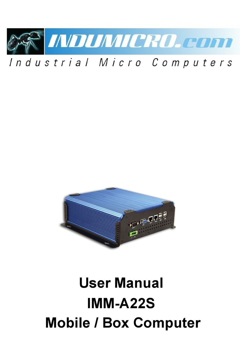
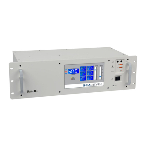
Indumicro IMM-L35PS User manual

Warning!
___________________________________
This equipment generates, uses and can radiate radio frequency energy and if not installed and
used in accordance with the instructions manual may cause interference to radio communications.
It has been tested and found to comply with the limits for a Class A computing device pursuant to
FCC Rules, which are designed to provide reasonable protection against such interference when
operated in a commercial environment. Operation of this equipment in a residential area is likely
to cause interference in which case the user at his own expense will be required to take whatever
measures may be required to correct the interference.
Disclaimer
This information in this document is subject to change without notice. In no event shall
Indumicro.com be liable for damages of any kind, whether incidental or consequential,
arising from either the use or misuse of information in this document or in any related
materials.
Electric Shock Hazard – Do not operate the machine with its back cover removed. There are
dangerous high voltages inside.
___________________________________

Table of Contents
Chapter 1: Introduction 1
System Specication . . . . . . . . . . . . . . . . . . . . . . . . . . . . . . . . . . . . . . . . . . . 1
Chapter 2: System Components 2
System Drawing . . . . . . . . . . . . . . . . . . . . . . . . . . . . . . . . . . . . . . . . . . . . . . 2
Block Diagram . . . . . . . . . . . . . . . . . . . . . . . . . . . . . . . . . . . . . . . . . . . . . . . 3
Front Components. . . . . . . . . . . . . . . . . . . . . . . . . . . . . . . . . . . . . . . . . . . . . 4
Rear Components . . . . . . . . . . . . . . . . . . . . . . . . . . . . . . . . . . . . . . . . . . . . . 5
Chapter 3: Board Layout 6
Connectors . . . . . . . . . . . . . . . . . . . . . . . . . . . . . . . . . . . . . . . . . . . . . . . . . 6
External Connectors. . . . . . . . . . . . . . . . . . . . . . . . . . . . . . . . . . . . . . . . . . . . 7
Internal Connectors and Jumpers . . . . . . . . . . . . . . . . . . . . . . . . . . . . . . . . . . . 8
Internal Connectors and Jumpers (backside) . . . . . . . . . . . . . . . . . . . . . . . . . . . . 9
Connectors and Jumpers List. . . . . . . . . . . . . . . . . . . . . . . . . . . . . . . . . . . . . .10
Jumper Settings . . . . . . . . . . . . . . . . . . . . . . . . . . . . . . . . . . . . . . . . . . . . . .11
Chapter 4: Hardware Setup 17
Preparing the Hardware Installation. . . . . . . . . . . . . . . . . . . . . . . . . . . . . . . . . .17
Installing the System Memory . . . . . . . . . . . . . . . . . . . . . . . . . . . . . . . . . . . . .17
Wireless Module Installation . . . . . . . . . . . . . . . . . . . . . . . . . . . . . . . . . . . . . .18
3G SIM Card Installation . . . . . . . . . . . . . . . . . . . . . . . . . . . . . . . . . . . . . . . . .18
PCI/PCIe Riser Card Installation . . . . . . . . . . . . . . . . . . . . . . . . . . . . . . . . . . . . .18
Connecting Power . . . . . . . . . . . . . . . . . . . . . . . . . . . . . . . . . . . . . . . . . . . . .19
Wall Mounting . . . . . . . . . . . . . . . . . . . . . . . . . . . . . . . . . . . . . . . . . . . . . . .19
Installing the Hard Disk . . . . . . . . . . . . . . . . . . . . . . . . . . . . . . . . . . . . . . . . . .19

Introduction
The IMM-L35PS features an Intel i5 2.5 GHz processor. It
has dual LAN as well as HDMI and DVI-D connectors for
high demand of Internet and video playback applications.
The IMM-L35PS also offers a variety of different expansion
opportunities to further customize the platform.
The following highlights the functionalities of the
IMM-L35PS system:
•Intel HD Graphics Engine
Dual video output of VGA and HDMI or VGA and DVI-D
•
with Intel integrated HD graphic engine
Dual 10/100/1000 Mbps LAN
•
USB x 6 (2 by internal pin header) and COM x 2
•
1 SATA 6Gbps HDD bay support and 1 SATA-DOM
•
connector
Totally 2 serial ports supporting Hardware Auto flow
•
Control: DB9 x2 for RS232/422/485
Audio input and output through Mic-in and Line-out
•
jack
Dual Mini-PCIe Socket (with on SIM card reader for 3G
•
wireless Internet connection) can extend the capability
for Wi-Fi or Bluetooth
Aluminum extrusion enclosure which helps heat
•
dissipation
System Specification
One PCIe expansion slot
•
Chapter 1: Introduction
IMM-L35PS User Manual
Dimensions (WxHxD) 277 x 67 x 194mm
(10.91” x 2.64” x 7.64”)
Processor Intel Core i5 2.5GHz
Chipset Intel HM65
System
Memory
DDR3 SO-DIMM x2
Up to 16GB
Storage
IDE N/A
SATA2.5” SSD/HDD drive bay x1,
SATA-DOM x1
Ethernet Controller Intel 82574L x2
Graphic Controller Intel integrated HD graphic engine
Audio Controller ALC886
IO
LAN RJ45 10/100/1000Mbps x2
Display
Dual Display
HDMI x1, DCI-D x1, VGA x1
VGA+HDMI, VGA+DVI
Clone, Independent, Extend
Audio Phone Jack x2 for Mic-In and Line-Out
DB9 x2 for RS232./422/485
Digital I/O DB9 Female x1 for DI x4 &DO x4 (TTL,
DO Max 100ma) - optional
Type A x6
Terminal Block 2-pin
Expansion
Mini-PCIe x1 with SIM card reader
Mini-PCIe x1
PCIe (x1) x 1
Power Input +9~+30v Input, Suppots ATX Function
Hardware Monitor Fintek F81865 integrated
Watchdog Timer 1~255 level
OS Support
Win7/XP/7Embedded/XP Embed-
ded, Redhat Enterprise 5/Fedora
14, Linux Kernel 2.6.18 or Later
Certications CE, FCC Class A
Operating Temperature
Range
-5~45°C / 23~113°F
Ordering Information
IMM-L35PS
Intel Core i5 2.5GHz on-board CPU,
2GB DDR3 SO-DIMM,
2 COM Ports,
1 HDMI, 1 DVI-D, 1 VGA, Audio Ports,
2 LAN Ports, DIO (4 in, 4 out),
+9~30V DC input support
250GB Hard Disk,
Technology
Max. Capacity
Dual Display Mode
Serial I/O
USB 2.0
Power Input
1

System Drawing
Mechanical dimensions of the IMM-L35PS
Unit: mm
Chapter 2: System Components
2
IMM-L35PS User Manual

Block Diagram
The block diagram depicts the relationships among the
interfaces and modules on the motherboard..
PCH
HM65
Processor
Intel
Sandy Bridge series
(BGA)
DMI2 x4
DDR3 1066/1333/1600
2x SO-DIMM up to 16GB
Fintek
F81865F
H/W Monitor
WDT RS-232/422/485
2x DB-9
P/S2 KB/MS
Pin Header
SATA Port 0
SATA Port 1
USB
Flash BIOS
SPI
Mini PCI Express
2x Socket
Wifi Card
GbELAN
Intel 82574L
2x PCIe 2x RJ-45
USB 2.0
4x Port-A (front I/O)
2x Port-A (rear I/O)
2x Pin Header
SATA Connector
2x 6 Gbps
PCIe x2
USB x2
VGA
Up to 2048x1536
DVI-D
Up to 1920x1200
Port C
HDMI
Up to 1920x1200
Port D
3G Card +
SIM Card Reader
LPC
PCIe Expansion
For Riser Board (pin header)
PEG
audio & serial board
Serial
Intel HD
Audio In/Out
1/8 Phone Jack
Audio Codec
ALC 886
PCIe x1 Slot
Voltage
Thermal
Sensor
2x PCIe !x
USB x2
Multi I/O Function
UART X4
Digital I/O x4
USB x2
PCIe x2
HD Audio
SATA x1
3.3V/5V/V1.5V/12V
IR remote
Receiver
(Optional)
Chapter 2: System Components
3
IMM-L35PS User Manual

Front Components
Component Description Pin Definition Reference
F1 ATX Power-on button with LEDs:
Standby mode in Red
Power-on mode in Green
F2
HDD LED (Yellow)
HDD
Blinking: data access activities
•
Off: no data access activities
•
Power
On: The computer is on.
•
Off: The computer is off .
•
F3 An USB type A connector. In addi-
•
tion to this connector, an internal
pin header is also provided.
USB1, USB2 on Page 13
F4 Reset Reset switch RST1 on page 15
F1 F2 F3 F4
•
•
Power Button with dual LED
Power LED (Green)
Four USB 2.0 Ports
Chapter 2: System Components
4
IMM-L35PS User Manual

Rear Components
Component Description Pin Definition Reference
R1
DC-in (power) 2-pin connector
Power-in Connector.
The system supports power range
between +9~+30V DC.
CN4 on page 15
R2An USB type A connector. In addition to
this connector, an internal pin header is
also provided..
USB3 Connector on Page 13
R3 Two RJ-45 (network) jacks with LED
indicators as described below. The LAN
ports are provided by Intel 82574L.
They both support WOL/Remote-
wake-up/PXE function.
LINK/ACT (Yellow)
On/Flashing: The port is linking
•
and active in data transmission.
Off: The port is not linking.
•
SPEED (Green/Amber)
Amber: The connection speed is
•
1000Mbps.
Green: The connection speed is
•
100Mbps
Off: The connection speed is
•
10Mbps.
LAN1/LAN2 on page 16
R4
DVI-D
A DVI-D port (single link) which is
provided by Intel HD Graphic Engine.
This port can support up to 1920x1200
@ 60 Hz resolution.
DVID1 Connectors on page 14
R5A HDMI (High-Definition Multimedia
Interface).This port can support up to
1920x1200 @ 60 Hz resolution.
HDMI1 on page 14
R6
VGA Port(*) The displays can support VGA up to
2048x1536 resolution.
VGA1 on page 14
R7Connect the audio devices to these
ports. The Microphone and line out
port are provided by Realtek ALC
ALC886.
CN1, CN2 on page 11
R8Serial ports through the DB-9
connector; Both COM1 and COM2
support RS-232/422/485 with jumper
selection among RS-232/422/485.
COM1/COM2 on page 11
R9 The PCIe/PCI expansion capability
is accomplished via the riser card
connected to the system
PCIEIO1 Connector on page 14
*Note that the driver for these ports should be installed with the following order: Chipset INF->Graphic->Audio
R9
R2 R6
R1
SPEED
LINK/ACT
R3 R5
R4
R7
R8
Two USB 2.0 Ports
Two 10/100/1000Mbps LAN
ports
HDMI
MIC IN/LINE OUT(*)
Serial Ports
Slot for PCIe expansion
Chapter 2: System Components
5
IMM-L35PS User Manual

Connectors
The following picture highlights the location of the COM
port and audio expansion card. Refer to the table 3.1
Connector List for more details.
COM1
COM2
CN1 CN2
SCT2
SCT1
JP1
SCT4
SCT3
JP2
COM-port and Audio Expansion Board
Chapter 3: Board Layout
6
IMM-L35PS User Manual

External Connectors
The following picture highlights the location of system
input/output connectors. Refer to the table 3.2 Connector
List for more details.
DVID1
USB1
LAN1/LAN2
HDMI1
USB3
USB2 RST1
VGA1 CN4
POWER1
LED1
CN3/
DCJK1
(optional)
IMM-L35PS Main Board
Chapter 3: Board Layout
7
IMM-L35PS User Manual

Internal Connectors and Jumpers
The following picture highlights the location of internal
connectors and jumpers. Refer to the table 3.2 Connector
List for more details.
LPC1
MPCIE1
FAN2
USB4
SIM1
SO-DIMM
SPI1
FRONT1
CMOS2
J1
MPCIE2
FAN1
CMOS1
SATA_PW2
Ignition1
COMSLT2
COMSLT1
IMM-L35PS Main Board
Chapter 3: Board Layout
8
IMM-L35PS User Manual

Internal Connectors and Jumpers
(backside)
The following picture highlights the location of internal
connectors and jumpers on the backside of the board.
Refer to the table 3.2 Connector List for more details.
SATA1
SATA2
PCIEIO1
PWR1
MIO1
IMM-L35PS Main Board
Chapter 3: Board Layout
9
IMM-L35PS User Manual

Connectors and Jumpers List
The tables below list the function of each of the board
jumpers and connectors by labels shown in the above
section. The next section in this chapter gives pin
definitions and instructions on setting jumpers.
Table 3.1 Connector List for the COM port and Audio expansion board
Labels Function Pin Denition Reference
Page
CN1 Microphone-in Audio Jack P11
CN2 Line-out Audio Jack P11
COM1 RS232/422/485 Serial Port P11
COM2 RS232/422/485 Serial Port P11
MIO1 Connector for connecting the COM port and
audio expansion board to the IMM-L35PS main
board
P12
SCT1/SCT2 Select COM1 Protocol Setting P11
SCT3/SCT4 Select COM2 Protocol Setting P11
JP1 Select COM1 Pin No. 9 function P12
JP2 Select COM2 Pin No. 9 function P12
Table 3.2 Connector List for IMM-L35PS Main Board
Labels Function Pin Denition Reference
Page
CMOS1 Clearing CMOS data including RTC P12
CMOS2 Clearing CMOS data only P12
CN3 (optional) Optional Power Connector with Power
-ignition Control
P16
CN4 DC-in Power Connector P15
DCJK1 (optional) Optional DC Jack type of Power Connector P16
DVID1 DVI-D Connector P14
FAN1/FAN2 System Fan Connector P14
Front1 Front Panel Function Pin Header P13
HDMI1 HDMI Port P14
Ignition1(optional) Connector for power Ignition Control P16
J1 PEG16X Lane Function Selection P15
LAN1/LAN2 Ethernet Connector 1/Ethernet Connector 2 P16
LPC1 Low Pin Count Interface Reserved for factory use
MIO1 COM and Audio Expansion Card Connector P12
MPCIE1 Mini-PCIe Connector P15
MPCIE2 Mini-PCIe Connector P15
PCIEIO1 PCI/PCIE Expansion connector for PCI or PCIe
low prole card (PCIEIO1, on the backside)
P14
PWR1 SATA Power Connector P13
RST1 Reset Button P15
SATA1/SATA2 Serial-ATA Connector (SATA2 supports SATA-
DOM)
P12
SATA_PW2 Switch for SATA port 2 power state P16
SIM1 SIM Card Reader P13
SPI1 Serial Peripheral Interface Bus Reserved for factory use
USB1/USB2/USB3 USB Type A Connector #0,1; #2,3; #4,5 P13
USB4 USB Pin Header P13
VGA1 VGA Port P14
Chapter 3: Board Layout
10
IMM-L35PS User Manual

SCT1, SCT2: Select COM1 Protocol Setting
RS-232
RS-422
RS-485
Switch
Protocol
SCT1 SCT2
RS-232 (default) 1-5, 2-6, 3-7, 4-8 1-2
RS-422 5-9, 6-10, 7-11, 8-12 3-4
RS-485 5-9, 6-10, 7-11, 8-12 5-6
SCT3, SCT4: Select COM2 Protocol Setting
Switch
Protocol
SCT3 SCT4
RS-232 (default) 1-5, 2-6, 3-7, 4-8 1-2
RS-422 5-9, 6-10, 7-11, 8-12 3-4
RS-485 5-9, 6-10, 7-11, 8-12 5-6
Jumper Settings
Microphone-in Audio Jack (CN1)
Line-out Audio Jack (CN2)
Note: The driver for the VGA and Audio ports
should be installed with the following order:
Chipset INF->Graphic->Audio
COM1 RS-232 Serial Port(COM1): It is a RS-232/422/485
port through the D-SUB9 connector.
RS-232/422/485SerialPort(COM2):ItisaRS-232/422/485
port through the D-SUB9 connector.
6789
12345
Pin No. Function
1CO_GND
2 MIC_INL
3CO_GND
4 INSULATOR
5 MIC_INR
Pin No. Pin Name
RS-232 RS-422 RS-485
1 DCD TXD- DATA-
2 RXD TXD+ DATA+
3 TXD RXD+
4 DTR RXD-
5 GND
6 DSR
7 RTS
8 CTS
9 RI
Pin No. Function
1CO_GND
2 LINOUT-L
3CO_GND
4 INSULATOR
5 LINOUT- R
Pin No. Pin Name
RS-232 RS-422 RS-485
1 DCD TXD- DATA-
2 RXD TXD+ DATA+
3 TXD RXD+
4 DTR RXD-
5 GND
6 DSR
7 RTS
8 CTS
9 RI
SCT2
1
3
5
2
4
6
SCT1
9
5
1
12
8
4
9
5
1
12
8
4
1
3
5
2
4
6
1
3
5
2
4
6
1
3
5
2
4
6
9
5
1
12
8
4
9
5
1
12
8
4
SCT3
1
2
3
4
9
10
11
12
SCT4
1
3
5
2
4
6
COM port and Audio expansion board
Chapter 3: Board Layout
11
IMM-L35PS User Manual

JP1, JP2: Select COM1 and COM2 Pin No9 (Ring Indicator)
function respectively
JP1 JP2
Pin Signal Pin Signal
1-2 VCC5 1-2 VCC5
3-4 VCC12 3-4 VCC12
5-6 SPI_RI 5-6 SPI_RI
MIO1 on the expansion card: Connector for connecting
the COM port and audio expansion board to the IMM-L35PS
main board.
PIN Pin Name PIN Pin Name
1GND 51 HDA_BCLK
2 N/A 52 HDA_SYNC
3 N/A 53 HDA_RST
4 GND 54 HDA_SDIN0
5 N/A 55 HDA_SDO
6 N/A 56 SPK
7 GND 57 GND
8 VCC5 58 VCC3
9 VCC5 59 VCC3
10 N/A 60 N/A
11 GND 61 GND
12 N/A 62 N/A
13 N/A 63 N/A
14 N/A 64 N/A
15 N/A 65 N/A
16 N/A 66 N/A
17 N/A 67 N/A
18 GND 68 GND
19 N/A 69 N/A
20 N/A 70 N/A
21 GND 71 N/A
22 +12V 72 N/A
23 N/A 73 N/A
24 VCC5 74 N/A
25 VCC5 75 GND
26 VCC5 76 N/A
27 VCC5 77 N/A
28 GND 78 GND
29 N/A 79 N/A
30 N/A 80 N/A
31 N/A 81 N/A
32 N/A 82 N/A
33 GND 83 GND
34 N/A 84 COM1_DCD#
35 N/A 85 COM1_RI#
36 N/A 86 COM1_CTS#
37 N/A 87 COM1_DTR#
38 N/A 88 COM1_RTS#
39 N/A 89 COM1_DSR#
40 N/A 90 COM1_SOUT
41 N/A 91 COM1_SIN
42 GND 92 GND
43 N/A 93 COM2_DCD#
44 N/A 94 COM2_RI#
45 N/A 95 COM2_CTS#
46 N/A 96 COM2_DTR#
47 N/A 97 COM2_RTS#
48 N/A 98 COM2_DSR#
49 N/A 99 COM2_SOUT
50 N/A 100 COM2_SIN
Clear CMOS jumper (CMOS1/CMOS2): It is for clearing
the CMOS data. CMOS 1clears CMOS data with real-time
clock (RTC) whereas CMOS2 clears CMOS data only.
To erase the CMOS data:
Turn off the computer and unplug the power cord.
Move the jumper cap from pins 1-2(default) to pins
1.
2-3. Keep the cap on pins 2-3 for about 5-10 seconds,
then move the cap back to pins 1-2.
Plug the power cord and turn on the computer.
2.
Enter BIOS setup to re-enter data.
3.
Serial-ATA Connector (SATA1/SATA2): It is for connecting
a 2.5’’ hard disk to be served as your system’s storage. It
can support SATA II which features Data transfer rates up
to 6.0 Gb/s (600 MB/s). SATA 2 connector also supports
SATA-DOM (the power line of SATA-DOM can be disabled
with a jumper on, see SATA_PW2).
Pin No. Pin Name
1-2 Normal (Default)
2-3 Clear CMOS and RTC (CMOS1)
Clear CMOS only (CMOS2)
1
2
3
1
3
5
2
4
6
Pin No. Function
1GND
2 TX0_P
3 TX0_N
4GND
5 RX0_N
6 RX0_P
7GND
1 2 3 4 5 6 7
7 6 5 4 3 2 1
SATA1
SATA2
Pin No. Function
1GND
2 TX1_P
3 TX1_N
4GND
5 RX1_N
6 RX1_P
7 VCC5
IMM-L35PS Main Board
12
Chapter 3: Board Layout
IMM-L35PS User Manual

Front Panel Function Pin Header (FRONT1): It provides
LED signal and button function on the front panel.
Mini PCI Express Connector (MIO1) on the mainboard:
COM and Audio Expansion Card Connector
PIN Pin Name PIN Pin Name
1GND 51 HDA_BCLK
2 SATATXN2 52 HDA_SYNC
3 SATATXP2 53 HDA_RST
4 GND 54 HDA_SDIN0
5 SATARXN2 55 HDA_SDO
6 SATARXP2 56 SPK
7 GND 57 VCC3_SB
8 VCC3P3_PS 58 VCC3_SB
9 VCC3P3_PS 59 VCC3_SB
10 VCC3P3_PS 60 VCC3_SB
11 GND 61 VCC3_SB
12 PCIE_RXN5 62 PCIE_RXN6
13 PCIE_RXP5 63 PCIE_RXP6
14 PCIE_TXN5 64 PCIE_TXN6
15 PCIE_TXP5 65 PCIE_TXP6
16 PCIE_CKN5 66 PCIE_CKN6
17 PCIE_CKP5 67 PCIE_CKP6
18 IGN_DI2 68 IGN_DI1
19 PLTRST 69 SMBCLK_
20 WAKE_N 70 SMBDATA
21 DCIN_VCC 71 REMOTE_POWER_
ON
22 VCC12_PS 72 3G_POWER_ON
23 VCC5_SB 73 USB_N12
24 VCC5_SB 74 USB_P12
25 VCC5 75 GND
26 VCC5 76 USB_N13
27 VCC5 77 USB_P13
28 GND 78 GND
29 DGOUT_0 79 DGIN_0
30 DGOUT_1 80 DGIN_1
31 DGOUT_2 81 DGIN_2
32 DGOUT_3 82 DGIN_3
33 GND 83 GND
34 COM3_DCD# 84 COM1_DCD#
35 COM3_RI# 85 COM1_RI#
36 COM3_CTS# 86 COM1_CTS#
37 COM3_DTR# 87 COM1_DTR#
38 COM3_RTS# 88 COM1_RTS#
39 COM3_DSR# 89 COM1_DSR#
40 COM3_SOUT 90 COM1_SOUT
41 COM3_SIN 91 COM1_SIN
42 GND 92 GND
43 COM4_DCD# 93 COM2_DCD#
44 COM4_RI# 94 COM2_RI#
45 COM4_CTS# 95 COM2_CTS#
46 COM4_DTR# 96 COM2_DTR#
47 COM4_RTS# 97 COM2_RTS#
48 COM4_DSR# 98 COM2_DSR#
49 COM4_SOUT 99 COM2_SOUT
50 COM4_SIN 100 COM2_SIN
The controller contains two modes of operation—a
legacy mode using I/O space, and an AHCI mode using
memory space. Software that uses legacy mode will not
have AHCI capabilities.
The AHCI ( Advanced Host Controller Interface) is a
programming interface which defines transactions
between the SATA controller and software and enables
advanced performance and usability with SATA. Platforms
supporting AHCI may take advantage of performance
features such as no master/slave designation for SATA
devices—each device is treated as a master—and
hardware assisted native command queuing. AHCI also
provides usability enhancements such as Hot-Plug.
Use the BIOS menu to configure your hard disk
to be AHCI compatible.
4-pin Serial-ATA Power Connector (PWR1): It is for
connecting the SATA power cord.
Dual USB 2.0 Port Connector #0 and #1 (USB1)
Dual USB 2.0 Port Connector #2 and #3 (USB2)
Dual USB 2.0 Port Connector #4 and #5 (USB3)
USB 2.0 Pin Header (USB4):
SIM Card Socket (SIM1):
10
8
6
4
2
9
7
5
3
1
Pin No. Description
C1 UIM_PWR
C2 UIM_RST
C3 UIM_CLK
C5 GND
C6 UIM_VPP
C7 UIM_DAT
C5 C7
C1 C3
1 2 3 4
5 6 7 8
Pin No. Pin Name
1VCCUSB
2 USB0N
3 USB0P
4 GND
5 VCCUSB1
6 USB1N
7 USB1P
8 GND
Pin No. Pin Name
1VCCUSB10
3 N/A
5USB10N
7 USB10P
9 GND
Pin No. Pin Name
2GND
4 USB11P
6 USB11N
8 N/A
10 VCCUSB11
1
3
5
7
9
2
4
6
8
10
Pin No. Function
1 +12V
2GND
3 GND
4 +5V
4 3 2 1
Pin No. Pin Name Function Pin No. Pin Name Function
1HD_LED+ HDD LED 2 PWR_LED+ Power LED
3 HD_LED- 4 PWR_LED-
5 Reset System Reset
Button
6 POWER_BTN Power On/Off
Push Button
7GND 8 GND
Chapter 3: Board Layout
13
IMM-L35PS User Manual

DVI-D Connector (DVID1): A single link DVI-D Connector
Pin No. Description Pin No. Description
1 TXD_2- 2 TXD_2+
3 GND 4 N/A
5 N/A 6 DDC_CLK
7 DDC_DATA 8 N/A
9TXD_1- 10 TXD_1+
11 GND 12 N/A
13 N/A 14 VCC5
15 GND 16 HPD
17 TXD_0- 18 TXD_0+
19 GND 20 N/A
21 N/A 22 GND
23 TXD_CLK_P 24 TXD_CLK_N
HDMI Connector (HDMI1): An HDMI Connector
Pin No. Description Pin No. Description
1 HDMI_DATP2_P 2 GND
3 HDMI_DATP2_N 4 HDMI_DATP1_P
5 GND 6 HDMI_DATP1_N
7 HDMI_DATP0_P 8 GND
9 HDMI_DATP0_N 10 HDMI_CLK_P
11 GND 12 HDMI_CLK_N
13 N/A 14 N/A
15 HDMI_DDC_CLK 16 HDMI_DDC_DAT
17 GND 18 PHDMI
19 HDMI_HPD
VGA (VGA1)
Pin Signal Pin Signal Pin Signal
1 RED 6 CRT DET 11 N/A
2 GREEN 7 GND 12 DDC DAT
3 BLUE 8 GND 13 HSYNC
4 N/A 9 VCC5 14 VSYNC
5 GND 10 GND 15 DDC CLK
Note: The driver for the VGA and Audio ports
should be installed with the following order:
Chipset INF->Graphic->Audio
System FAN Connector (FAN1/FAN2)
Pin No. Description
1 GND
2 VCC5
3 FAN TAC
PCIe Expansion connector for PCIe low profile card
(PCIEIO1, on the backside)
PIN SIGNAL PIN SIGNAL PIN SIGNAL
1 VCC3P3_SB 53 PCIE_CKP1 105 PEG_RXP9
2 VCC5_SB 54 PCIE_TXP1 106 PEG_TXP9
3 VCC3P3_SB 55 PCIE_CKN1 107 GND
4 VCC5_SB 56 PCIE_TXN1 108 GND
5 N/A 57 GND 109 PEG_RXN8
6 N/A 58 GND 110 PEG_TXN8
7 VCC3P3_ 59 PEGACLKN 111 PEG_RXP8
8 V1P5 60 PEGBCLKN 112 PEG_TXP8
9 VCC3P3_ 61 PEGACLKP 113 GND
10 N/A 62 PEGBCLKP 114 GND
11 VCC3P3_ 63 GND 115 PEG_RXN7
12 VCC5 64 GND 116 PEG_TXN7
13 VCC3P3_ 65 GND 117 PEG_RXP7
14 VCC5 66 GND 118 PEG_TXP7
15 VCC3P3_ 67 PEG_RXN15 119 GND
16 VCC5 68 PEG_TXN15 120 GND
17 VCC3P3_ 69 PEG_RXP15 121 PEG_RXN6
18 VCC5 70 PEG_TXP15 122 PEG_TXN6
19 N/A 71 GND 123 PEG_RXP6
20 VCC5 72 GND 124 PEG_TXP6
21 GND 73 PEG_RXN14 125 GND
22 VCC5 74 PEG_TXN14 126 GND
23 N/A 75 PEG_RXP14 127 PEG_RXN5
24 N/A 76 PEG_TXP14 128 PEG_TXN5
25 +12V 77 GND 129 PEG_RXP5
26 GND 78 GND 130 PEG_TXP5
27 +12V 79 PEG_RXN13 131 GND
28 GND 80 PEG_TXN13 132 GND
29 +12V 81 PEG_RXP13 133 PEG_RXN4
30 CLKRQ1 82 PEG_TXP13 134 PEG_TXN4
31 +12V 83 GND 135 PEG_RXP4
32 CLKRQ2 84 GND 136 PEG_TXP4
33 N/A 85 PEG_RXN12 137 GND
34 GND 86 PEG_TXN12 138 GND
35 PLTRST 87 PEG_RXP12 139 PEG_RXN3
36 SMBCLK 88 PEG_TXP12 140 PEG_TXN3
37 WAKE_N 89 GND 141 PEG_RXP3
38 SMBDATA 90 GND 142 PEG_TXP3
1
159
2
160
3 2 1
FAN1
3
2
1
FAN2
15 14 13 12 11
5 4 3 2 1
14
Chapter 3: Board Layout
IMM-L35PS User Manual

MPCIE1: Mini-PCIe Connector with SIM Card Reader
Pin Signal Pin Signal
1 WAKE# 2 VCC3.3
3 N/A 4 GND
5 N/A 6 VCC1.5
7 CLKREQ# 8 USIM_PWR
9 GND 10 UIM_DATA
11 PCIE_CLK_N3 12 UIM_CLK
13 PCIE_CLK _P3 14 UIM_RESET
15 GND 16 UIM_VPP
17 RSV 18 GND
19 RSV 20 N/A
21 GND 22 PLTRST
23 PCIE_RX_N3 24 VCC3.3
25 PCIE_RX_P3 26 GND
27 GND 28 VCC1.5
29 GND 30 SMBCLK
31 PCIE_TX_N3 32 SMBDATA
33 PCIE_TX_P3 34 GND
35 GND 36 USB_N8
37 GND 38 USB_P8
39 VCC3.3 40 GND
41 VCC3.3 42 N/A
43 GND 44 N/A
45 RSV 46 N/A
47 RSV 48 VCC1.5
49 RSV 50 GND
51 RSV 52 VCC3.3
MPCIE2: Mini-PCIe Connector
Pin Signal Pin Signal
1 WAKE# 2 VCC3.3
3 N/A 4 GND
5 N/A 6 VCC1.5
7 CLKREQ# 8 N/A
9GND 10 N/A
11 PCIE_CLK _N4 12 N/A
13 PCIE_CLK _P4 14 N/A
15 GND 16 N/A
17 RSV 18 GND
19 RSV 20 N/A
21 GND 22 PLTRST
23 PCIE_RX_N4 24 VCC3.3
25 PCIE_RX_P4 26 GND
27 GND 28 VCC1.5
29 GND 30 SMBCLK
31 PCIE_TX_N4 32 SMBDATA
33 PCIE_TX_P4 34 GND
35 GND 36 USB_N9
37 GND 38 USB_P9
39 VCC3.3 40 GND
41 VCC3.3 42 N/A
43 GND 44 N/A
45 RSV 46 N/A
47 RSV 48 VCC1.5
49 RSV 50 GND
51 RSV 52 VCC3.3
PIN SIGNAL PIN SIGNAL PIN SIGNAL
39 GND 91 PEG_RXN11 143 GND
40 GND 92 PEG_TXN11 144 GND
41 PCIE_RXN2 93 PEG_RXP11 145 PEG_RXN2
42 PCIE_CKN2 94 PEG_TXP11 146 PEG_TXN2
43 PCIE_RXP2 95 GND 147 PEG_RXP2
44 PCIE_CKP2 96 GND 148 PEG_TXP2
45 GND 97 PEG_RXN10 149 GND
46 GND 98 PEG_TXN10 150 GND
47 PCIE_RXP1 99 PEG_RXP10 151 PEG_RXN1
48 PCIE_TXN2 100 PEG_TXP10 152 PEG_TXN1
49 PCIE_RXN1 101 GND 153 PEG_RXP1
50 PCIE_TXP2 102 GND 154 PEG_TXP1
51 GND 103 PEG_RXN9 155 GND
52 GND 104 PEG_TXN9 156 GND
157 PEG_RXN0
158 PEG_TXN0
159 PEG_RXP0
160 PEG_TXP0
Reset Button (RST1)
Pin NO. Description
1 RST_BTN
2 GND
3 GND
4 N/A
DC_IN CONNECTOR (CN4): A Phoenix connector for
external power supply.
J1(PEG 16X lane function): PCI/PCIe (PCIEIO1) expansion
connector signal selection
Pin Lane Function1 Function2
(1) (3)
H H
x16 DISABLE DISABLE
(1) (3-4)
H L
x8, x8 ENABLE DISABLE
(1-2) (3)
L H
Reserved DISABLE ENABLE
(1-2) (3-4)
L L
x8, x4, x4 ENABLE ENABLE
Pin No. Pin Name
1GND
2 DC_VIN
1
3
2
4
1 2
1
3
2
4
Chapter 3: Board Layout
15
IMM-L35PS User Manual

Ignition Connector on board (ignition1): Power
ignition connector.
SATA_PW2: A switch for supply of SATA Connector II’s
power.
CN3 (optional): An optional power connector with
power -ignition Control
DCJK1 (Optional): An optional DC Jack type of Power
Connector
LAN1/LAN2 Ports (LAN1/LAN2): The LAN ports are
provided by Intel 82574L Ethernet controller whose
interface complies with PCI-e 1.1 (2.5 Ghz). It has advanced
management features including IPMI pass-through via
SMBus or NC-SI, WOL, PXE remote boot, ISCSI boot and
VLAN filtering.
Pin No. Description
Fast Ethernet Gigabit Ethernet
1 TX+ BI_DA+
2TX- BI_DA-
3 RX+ BI_DB+
4 -- BI_DC+
5 -- BI_DC-
6RX- BI_DB-
7 -- BI_DD+
8 -- BI_DD-
Pin No. Pin Name
1 Ignition
2GND
3 DC_VIN
Pin No. Pin Name
1-2 SATAII Connector without power
2-3 SATA II Connector with 5V power
Pin No. Pin Name Pin No. Pin Name
1DCIN_VCC 6 DC2DC_PWROK
2 DC_VIN 7 COM5_SIN
3 GND 8 SOUT
4 SYS_PWROK 9 PWR_BTN_IGN
5DC2DC_EN 10 IGNITION
1 2 3 4 10
1
2
3
Pin No. Pin Name
1DC_VIN
2 GND
3 GND
1 2 3
16
Chapter 3: Board Layout
IMM-L35PS User Manual

Preparing the Hardware Installation
To access some components and perform certain service
procedures, you must perform the following procedures
first.
WARNING: To reduce the risk of personal injury,
electric shock, or damage to the equipment,
remove the power cord to remove power from
the server. The power switch button does not
completely shut off system power. Portions of the
power supply and some internal circuitry remain
active until power is removed.
Unpower the IMM-L35PS and remove the power cord.
1.
Unscrew the 4 threaded screws from the top cover.2.
Open the cover.
3.
Note:
If the CPU thermal pad breaks apart, use your
hands to reattach the parts and stick them
together.
Installing the System Memory
The motherboard supports DDR3 memory to meet the
higher bandwidth requirements of the latest operating
system and Internet applications. It comes with two
Double Data Rate Three (DDR3) Small Outline Dual Inline
Memory Module (SO-DIMM) socket.
Align the memory module’s cutout with the SO-DIMM
1.
socket’s notch.
Install the SO-DIMM.
2.
Note:
The system can support memory of DDR3 SO-
DIMM up to 16 GB in maximum with 2 SO-DIMM
sockets.
1
2
Chapter 4: Hardware Setup
17
IMM-L35PS User Manual
Table of contents
Other Indumicro Desktop manuals

