Innodisk InnoAGE M.2 (S80) 3TI7 User manual

M.2 (S80) 3TI7
Customer:
Customer
Part
Number:
Innodisk
Part
Number:
Innodisk
Model Name:
Date:
Innodisk
Approver
Customer
Approver

InnoAGETM
M.2 (S80) 3TI7
2 V1.2 TPS, July., 2020
Table of contents
LIST OF FIGURES ....................................................................................................................................................... 6
1. PRODUCT OVERVIEW ......................................................................................................................................... 7
1.1
INTRODUCTION OF INNODISK INNOAGE M.2 (S80) 3TI7 ............................................................. 7
1.2
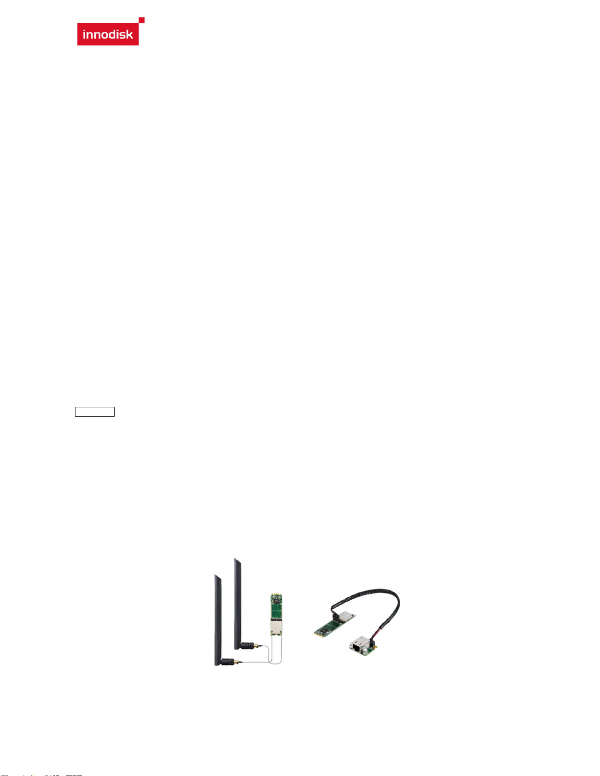
PRODUCT VIEW AND MODELS ............................................................................................................... 7
1.3 SATA INTERFACE ................................................................................................................................... 8
2. PRODUCT SPECIFICATIONS ........................................................................................................................... 9
2.1 CAPACITY AND DEVICE PARAMETERS ................................................................................................... 9
2.2 PERFORMANCE ...................................................................................................................................... 10
2.3 ELECTRICAL SPECIFICATIONS ............................................................................................................. 11
2.3.1 Power Requirement .......................................................................................................................... 11
2.3.2 Power Consumption ......................................................................................................................... 11
2.4 ENVIRONMENTAL SPECIFICATIONS .................................................................................................... 11
2.4.1 Temperature Ranges ....................................................................................................................... 11
2.4.2 Humidity .................................................................................................................................................. 11
2.4.3 Shock and Vibration ......................................................................................................................... 11
2.4.4 Mean Time between Failures (MTBF) .................................................................................... 12
2.5 CE AND FCC COMPATIBILITY ............................................................................................................. 12
2.6 ROHS COMPLIANCE ............................................................................................................................. 12
2.7 RELIABILITY ......................................................................................................................................... 12
2.8 TRANSFER MODE .................................................................................................................................. 13
2.9 PIN ASSIGNMENT ................................................................................................................................. 13
2.9.1 M.2 SATA PIN ASSIGNMENT .......................................................................................................... 13
2.9.2 INNOAGETM M.2 PIN HEADER DEFINITION ................................................................................... 14
2.10.1 INNOAGETM M.2 (S80) ............................................................................................................ 16
2.10.2 ETHERNET DAUGHTER BOARD ...................................................................................................... 16
2.11 ASSEMBLY WEIGHT ........................................................................................................................... 17
2.12 SEEK TIME .......................................................................................................................................... 17
2.13 HOT PLUG ........................................................................................................................................... 17
2.14 NAND FLASH MEMORY ..................................................................................................................... 17
3. THEORY OF OPERATION ................................................................................................................................. 18
3.3 MCU ...................................................................................................................................................... 18
3.11 DIE RAID .......................................................................................................................................... 22
3.12 HARDWARE-BASED 256-BIT AES ................................................................................................... 22
3.12.1 INNOAGE SSD WITH AES FLOW CHART ................................................................................... 22
3.12.2 ENCRYPTED KEY MANAGEMENT .................................................................................................... 22
3.12.3 AUTHORIZED KEY MANAGEMENT .................................................................................................. 23
3.12 FW RECOVERY FUNCTION*1 ............................................................................................................ 23

InnoAGETM
M.2 (S80) 3TI7
3 V1.2 TPS, July., 2020
3.13 QUICK ERASE ..................................................................................................................................... 24
3.14 WRITE PROTECT ................................................................................................................................ 24
3.15 SANITIZING INNOAGE SSD ............................................................................................................ 24
4.1 INNOAGE M.2 (S80) 3TI7 PIN DIRECTIONS ................................................................................ 26
4.2 ELECTRICAL CONNECTIONS FOR INNOAGE M.2 (S80) 3TI7 ....................................................... 26
4.3 DEVICE DRIVE ...................................................................................................................................... 26
5. SMART FEATURE SET ........................................................................................................................................ 27
5.1 SMART ATTRIBUTES ........................................................................................................................... 27
6. PART NUMBER RULE ......................................................................................................................................... 29
7. APPENDIX ............................................................................................................................................................... 30

InnoAGETM
M.2 (S80) 3TI7
4 V1.2 TPS, July., 2020
R
EVISION
H
ISTORY
Revision Description Date
V1.0 First Release Apr., 2020
V1.1 Correct part number July., 2020
V1.2 Correct the typo of pin header 2
Support Private Cloud
July., 2020

InnoAGETM
M.2 (S80) 3TI7
5 V1.2 TPS, July., 2020
List of Tables
TABLE 1: DEVICE PARAMETERS..................................................................................................................................... 9
TABLE 2: PERFORMANCE .............................................................................................................................................. 10
TABLE 3: INNODISK INNOAGE M.2 (S80) 3TI7 POWER REQUIREMENT..................................................... 11
TABLE 4: POWER CONSUMPTION ............................................................................................................................... 11
TABLE 5: TEMPERATURE RANGE FOR INNOAGE M.2 (S80) 3TI7 .................................................................. 11
TABLE 6: SHOCK/VIBRATION TESTING FOR INNOAGE M.2 (S80) 3TI7 .................................................... 11
TABLE 7: INNOAGE M.2 (S80) 3TI7 MTBF ....................................................................................................... 12
TABLE 8: INNOAGE M.2 (S80) 3TI7 TBW ......................................................................................................... 12
TABLE 9: INNODISK INNOAGE M.2 (S80) 3TI7 PIN ASSIGNMENT ............................................................. 13
TABLE 10: INNODISK INNOAGETM M.2 (S80) 3TI7 PIN HEADER 1 ASSIGNMENT .................................. 14
TABLE 11: INNODISK INNOAGETM M.2 (S80) 3TI7 PIN HEADER 2 ASSIGNMENT .................................. 15
TABLE 10: SMART COMMAND.................................................................................................................................... 27
TABLE 11: SMART ATTRIBUTE .................................................................................................................................. 27

InnoAGETM
M.2 (S80) 3TI7
6 V1.2 TPS, July., 2020
List of Figures
FIGURE 1: INNODISK INNOAGE M.2 (S80) 3TI7 ............................................................................................... 7
FIGURE 2: INNODISK INNOAGE M.2 (S80) 3TI7 BLOCK DIAGRAM ............................................................ 18
FIGURE 3: EDGE TO AZURE CLOUD SYSTEM ARCHITECTURE ............................................................................... 19
FIGURE 4: EDGE TO PRIVATE CLOUD SYSTEM ARCHITECTURE ........................................................................... 19
FIGURE 5: INNOAGE SSD PARTITIONED FOR FUTURE RECOVERY PURPOSES ................................................ 24
FIGURE 6: PC RESET PIN CONNECTION TO INNOAGE SSD BLOCK DIAGRAM ............................................... 24
FIGURE 7: ATA CRYPTOGRAPHIC ERASE COMMAND ............................................................................................. 25
FIGURE 8: SCREENSHOT OF INNOAGE SSD MANAGEMENT PLATFORM ............................................................ 25
FIGURE 9: SIGNAL SEGMENT AND POWER SEGMENT ............................................................................................ 26

InnoAGETM
M.2 (S80) 3TI7
7 V1.2 TPS, July., 2020
1. Product Overview
1.1 Introduction of Innodisk InnoAGE M.2 (S80) 3TI7
The InnoAGETM M.2 (S80) 3TI7 comes with a Microsoft Azure Sphere inside, and is further
integrated with Innodisk’s customized firmware, software, and hardware technology. This new
solution enables multifunctional management: smart data analysis and updates, data security,
and remote control through the cloud, while benefitting from the power of the Azure Sphere to
guarantee secured communications between the SSD and the cloud.
The InnoAGE™ M.2 (S80) 3TI7 delivers an easy-to-use interface with its customized cloud
management platform. In technical terms, the Innodisk-developed firmware receives commands
from the Azure Sphere via a second connection to Azure. Therefore, it is able to execute SSD
debugging messages as well as monitor read/write behavior patterns to increase the storage
device’s lifespan. Most importantly, system operators can quickly revert to the default settings
from the cloud-based dashboard in the case of a device or system crash.
In other words, the InnoAGE™ M.2 (S80) 3TI7 is designed for both in-band and out-of-band
network management, providing full recovery even when the operating system has crashed or is
severely impaired to the extent that in-band management would be of little help.
CAUTION TRIM must be enabled.
TRIM enables SSD’s controller to skip invalid data instead of moving. It can free up significant amount of
resources, extends the lifespan of SSD by reducing erase, and write cycles on the SSD. Innodisk’s handling
of garbage collection along with TRIM command improves write performance on SSDs.
1.2 Product View and Models
Innodisk InnoAGE M.2 (S80) 3TI7 is available in follow capacities within 3D TLC flash ICs.
InnoAGE M.2 (S80) 3TI7 64GB-512GB
Figure 1: Innodisk InnoAGE M.2 (S80) 3TI7

InnoAGETM
M.2 (S80) 3TI7
8 V1.2 TPS, July., 2020
1.3 SATA Interface
Innodisk InnoAGE M.2 (S80) 3TI7 supports SATA III interface, and compliant with SATA I and
SATA II. SATA III interface can work with Serial Attached SCSI (SAS) host system, which is used
in server computer. Innodisk InnoAGE M.2 (S80) 3TI7 is compliant with Serial ATA Gen 1, Gen 2
and Gen 3 specification (Gen 3 supports 1.5Gbps /3.0Gbps/6.0Gbps data rate).

InnoAGETM
M.2 (S80) 3TI7
9 V1.2 TPS, July., 2020
2. Product Specifications
2.1 Capacity and Device Parameters
InnoAGE M.2 (S80) 3TI7 device parameters are shown in Table 1.
Table 1: Device parameters
Capacity P/N OS back-up
capacity (GB)
LBA User
Capacity(GB)
64GB DTM28-64GDK1*1*2*3DF10G 10 96259888 45.9
DTM28-64GDK1*1*2*3DF20G 20 75288368 35.9
128GB
DTM28-A28DK1*1*2*3QF10G 10 213470128 101.7
DTM28-A28DK1*1*2*3QF20G 20 19249860 91.7
DTM28-A28DK1*1*2*3QF30G 30 171527088 81.7
DTM28-A28DK1*1*2*3QF40G 40 150555568 71.7
DTM28-A28DK1*1*2*3QF50G 50 129584048 61.7
256GB
DTM28-B56DK1*1*2*3QF10G 10 447890608 213.5
DTM28-B56DK1*1*2*3QF20G 20 426919088 203.5
DTM28-B56DK1*1*2*3QF30G 30 405947568 193.5
DTM28-B56DK1*1*2*3QF40G 40 384976048 183.5
DTM28-B56DK1*1*2*3QF50G 50 364004528 173.5
512GB
DTM28-C12DK1*1*2*3QF10G 10 916731568 437.1
DTM28-C12DK1*1*2*3QF20G 20 895760048 427.1
DTM28-C12DK1*1*2*3QF30G 30 874788528 417.1
DTM28-C12DK1*1*2*3QF40G 40 853817008 407.1
DTM28-C12DK1*1*2*3QF50G 50 832845488 397.1
1TB
DTM28-01TDK1*1*2*3QF10G 10 1854413488 884.2
DTM28-01TDK1*1*2*3QF20G 20 1833441968 874.2
DTM28-01TDK1*1*2*3QF30G 30 1812470448 864.2
DTM28-01TDK1*1*2*3QF40G 40 1791498928 854.2
DTM28-01TDK1*1*2*3QF50G 50 1770527408 844.2
Note
*1 E: Azure Cloud; J: Private Cloud
*2 C: standard temperature (0’C to 70’C); W: wide temperature (-40’C to 85’C)
*3 1: with Ethernet daughter board; 2: with Wi-Fi antenna

InnoAGETM
M.2 (S80) 3TI7
10 V1.2 TPS, July., 2020
2.2 Performance
Burst Transfer Rate: 6.0Gbps
Table 2: Performance
Capacity 32GB 64GB 128GB 256GB 512GB
Sequential*
Read (max.)
185 MB/s 370MB/s 550 MB/s 550 MB/s 540 MB/s
Sequential*
Write (max.)
30 MB/s 60 MB/s 125 MB/s 255 MB/s 315 MB/s
4KB Random*
Read (QD32)
13500
IOPS
25000
IOPS
48000
IOPS
70000
IOPS
61000
IOPS
4KB Random*
Write (QD32)
7700
IOPS
16000
IOPS
32000
IOPS
59000
IOPS
70000
IOPS
Note: *Performance results are measured in Room Temperature with Out-of-Box devices and may vary depending on
overall system setup.
** Performance results are based on CrystalDiskMark 6.0.0 with file size 1000MB of Queue Depth 32

InnoAGETM
M.2 (S80) 3TI7
11 V1.2 TPS, July., 2020
2.3 Electrical Specifications
2.3.1 Power Requirement
Table 3: Innodisk InnoAGE M.2 (S80) 3TI7 Power Requirement
Item Symbol Rating Unit
Input voltage VIN +3.3 DC +- 5% V
2.3.2 Power Consumption
Table 4: Power Consumption
Mode Power Consumption (mA)
Startup 590
Read 420
Write 490
Idle 245
* Target: 512GB InnoAGE M.2 (S80) 3TI7
2.4 Environmental Specifications
2.4.1 Temperature Ranges
Table 5: Temperature range for InnoAGE M.2 (S80) 3TI7
Temperature Range
Operating Standard Grade: 0°C to +70°C
Industrial Grade:-40°C to +85°C
Storage -55°C to +95°C
2.4.2 Humidity
Relative Humidity: 10-95%, non-condensing
2.4.3 Shock and Vibration
Table 6: Shock/Vibration Testing for InnoAGE M.2 (S80) 3TI7
Reliability Test Conditions Reference Standards
Vibration 7 Hz to 2K Hz, 20G, 3 axes IEC 68-2-6
Mechanical Shock
Duration: 0.5ms, 1500 G, 3 axes
IEC 68-2-27

InnoAGETM
M.2 (S80) 3TI7
12 V1.2 TPS, July., 2020
2.4.4 Mean Time between Failures (MTBF)
Table 7 summarizes the MTBF prediction results for various INNOAGE M.2 (S80) 3TI7
configurations. The analysis was performed using a RAM Commander™ failure rate prediction.
‧
Failure Rate: The total number of failures within an item population, divided by the total
number of life units expended by that population, during a particular measurement interval
under stated condition.
‧
Mean Time between Failures (MTBF): A basic measure of reliability for repairable items:
The mean number of life units during which all parts of the item perform within their specified
limits, during a particular measurement interval under stated conditions.
Table 7: InnoAGE M.2 (S80) 3TI7 MTBF
Product Condition MTBF (Hours)
Innodisk Inno
AGE M.2 (S80)
3TI7 Telcordia SR-332 GB, 25°C >3,000,000
2.5 CE and FCC Compatibility
InnoAGE M.2 (S80) 3TI7 conforms to CE and FCC requirements.
2.6 RoHS Compliance
InnoAGE M.2 (S80) 3TI7 is fully compliant with RoHS directive.
2.7 Reliability
Table 8: InnoAGE M.2 (S80) 3TI7 TBW
Parameter Value
Read Cycles Unlimited Read Cycles
Flash endurance 3,000 P/E cycles
Wear-Leveling Algorithm Support
Bad Blocks Management Support
Error Correct Code Support
TBW* (Total Bytes Written)
Unit:
TB
Capacity Sequential workload Client workload
32GB 84.3 37.5
64GB 168.6 75
128GB 337.2 150
256GB 674.4 250
512GB 1348.8 500
* Note:
1. Sequential: Mainly sequential write, tested by Vdbench.
2. Client: Follow JESD218 Test method and JESD219A Workload, tested by
ULINK. (The capacity lower than 64GB client workload is not specified in
JEDEC219A, the values are estimated.)
3. Based on out-of-box performance.

InnoAGETM
M.2 (S80) 3TI7
13 V1.2 TPS, July., 2020
2.8 Transfer Mode
InnoAGE M.2 (S80) 3TI7 support following transfer mode:
Serial ATA III 6.0Gbps
Serial ATA II 3.0Gbps
Serial ATA I 1.5Gbps
2.9 Pin Assignment
2.9.1 M.2 SATA pin assignment
Innodisk InnoAGE M.2 (S80) 3TI7 uses a standard SATA pin-out. See Table 9 for InnoAGE M.2
(S80) 3TI7 pin assignment.
Table 9: Innodisk InnoAGE M.2 (S80) 3TI7 Pin Assignment
Signal Name Pin #
Pin # Signal Name
75 GND
3.3V 74 73 GND
3.3V 72 71 GND
3.3V 70 69 GND
NC 68 67 NC
Notch 66 65 Notch
Notch 64 63 Notch
Notch 62 61 Notch
Notch 60 59 Notch
NC 58
NC 56 57 GND
NC 54 55 NC
NC 52 53 NC
NC 50 51 GND
NC 48 49 RX+
NC 46 47 RX-
NC 44 45 GND
NC 42 43 TX-
NC 40 41 TX+
NC 38 39 GND
NC 36 37 NC
NC 34 35 NC
NC 32 33 GND
NC 30 31 NC
NC 28 29 NC

InnoAGETM
M.2 (S80) 3TI7
14 V1.2 TPS, July., 2020
NC 26 27 GND
NC 24 25 NC
NC 22 23 NC
NC 20 21 GND
Notch 18 19 Notch
Notch 16 17 Notch
Notch 14 15 Notch
Notch 12 13 Notch
DAS/DSS 10 11 NC
NC 8 9 NC
NC 6 7 NC
3.3V 4 5 NC
3.3V 2 3 GND
1 GND
2.9.2 InnoAGE
TM
M.2 pin header definition
Pin header 1 is assigned for trigger PC reset function, while the OS recovery is finished, it will
be automatically send commend to notify PC to re-boot power. In addition, InnoAGETM SSD
reserves external GPIO pins to connect with system for customized application. Pin header 2 is
design for connecting with daughter board from SPI to Ethernet. See table 10 and 11.
Table 10: Innodisk InnoAGETM M.2 (S80) 3TI7 Pin Header 1 Assignment
SSD control
MB reset
MB control SSD
Recovery
MB Power status
LED pin
MB SSD status
LED pin
SSD control MB
power button
(Optional)
H1/Pin 1 H1/Pin 3 H1/Pin 5 H1/Pin 7 H1/Pin 9
H1/Pin 2 H1/Pin 4 H1/Pin 6 H1/Pin 8 H1/Pin 10
GND GND GND GND GND
Pin Function Direction Notification
1
RC_RST* O Active low
GPIO I/O Bi-direction, function programmable
3 Recovery* I Active low

InnoAGETM
M.2 (S80) 3TI7
15 V1.2 TPS, July., 2020
GPIO I/O Interrupt-capable and bi-direction, function programmable
5
GPIO I/O Bi-direction, function programmable
TX O TX of UART, pair with pin 7
7
GPIO I/O Bi-direction, function programmable
RX I RX of UART, pair with pin 5
9
GPIO I/O Interrupt-capable and bi-direction, function programmable
PWM O PWM control, frequency/duty TBD
2/4/6/8/10 GND System GND
* Default setting function
VO range: -0.28<VOL<0.4; 2.4<VOH<3.63 (V)
VI range: -0.28<VIL<0.28; 2.0<VIH<3.63 (V)
Table 11: Innodisk InnoAGETM M.2 (S80) 3TI7 Pin Header 2 Assignment
INT MISO CLK RST GND
H2/Pin 1 H2/Pin 3 H2/Pin 5 H2/Pin 7 H2/Pin 9
H2/Pin 2 H2/Pin 4 H2/Pin 6 H2/Pin 8 H2/Pin 10
NC NC MOSI CS 3.3V
Pin Function Direction Notification
1
INT* I Interrupt-capable GPIO
PWM O PWM control, frequency/duty TBD
GPIO I/O Bi-direction, function programmable
3
MISO* I MISO of SPI interface, pair with pin 5/6/8
DATA I/O CLK of I2C interface, pair with pin5
RX I RX of UART, pair with pin 5/6/8
GPIO I/O Bi-direction, function programmable
5
CLK* O CLK of SPI interface, pair with pin 3/6/8
TX O TX of UART, pair with pin 3/6/8
GPIO I/O Bi-direction, function programmable
6
MOSI* O MOSI of SPI interface, pair with pin 3/5/8
CLK I/O CLK of I2C interface, pair with pin 3
RTS O RTS of UART, pair with pin 3/5/8
GPIO I/O Bi-direction, function programmable
7 RST I SSD module reset pin, active low
8
CS* O CS of SPI interface, pair with pin 3/5/6
CTS I CST of UART, pair with pin 3/5/6
GPIO I/O Bi-direction, function programmable

InnoAGETM
M.2 (S80) 3TI7
16 V1.2 TPS, July., 2020
10 3V3 System power 3.3V
9 GND System GND
2/4 NC No internal connection
* Default setting function
VO range: -0.28<VOL<0.4; 2.4<VOH<3.63 (V)
VI range: -0.28<VIL<0.28; 2.0<VIH<3.63 (V)
2.10 Mechanical Dimensions
2.10.1 InnoAGETM M.2 (S80)
2.10.2 Ethernet Daughter Board
Horizontal Type Vertical Type

InnoAGETM
M.2 (S80) 3TI7
17 V1.2 TPS, July., 2020
Cable Connection to Ethernet Daughter Board
2.11 Assembly Weight
An Innodisk InnoAGE M.2 (S80) 3TI7 within flash ICs, 64GB’s weight is 8 grams approximately.
2.12 Seek Time
Innodisk InnoAGE M.2 (S80) 3TI7 is not a magnetic rotating design. There is no seek or rotational
latency required.
2.13 Hot Plug
The SSD support hot plug function and can be removed or plugged-in during operation. User has
to avoid hot plugging the SSD which is configured as boot device and installed operation system.
Surprise hot plug : The insertion of a SATA device into a backplane (combine signal and power)
that has power present. The device powers up and initiates an OOB
sequence.
Surprise hot removal: The removal of a SATA device from a powered backplane, without first
being placed in a quiescent state.
2.14 NAND Flash Memory
Innodisk InnoAGE M.2 (S80) 3TI7 uses 3D Triple Level Cell (TLC) NAND flash memory, which is
non-volatility, high reliability and high speed memory storage.

InnoAGETM
M.2 (S80) 3TI7
18 V1.2 TPS, July., 2020
3. Theory of Operation
3.1 Overview
Figure 2 shows the operation of Innodisk InnoAGE M.2 (S80) 3TI7 from the system level, including
the major hardware blocks.
Figure 2: Innodisk InnoAGE M.2 (S80) 3TI7 Block Diagram
Innodisk InnoAGE M.2 (S80) 3TI7 integrates a SATA III controller and NAND flash memories.
Communication with the host occurs through the host interface, using the standard ATA protocol.
Communication with the flash device(s) occurs through the flash interface.
3.2 SATA III Controller
Innodisk InnoAGE M.2 (S80) 3TI7 is designed with a SATA III 6.0Gbps (Gen. 3) controller. The
Serial ATA physical, link and transport layers are compliant with Serial ATA Gen 1, Gen 2 and Gen
3 specification (Gen 3 supports 1.5Gbps/3.0Gbps/6.0Gbps data rate). The controller has 4
channels for flash interface.
3.3 MCU
Innodisk InnoAGE M.2 (S80) 3TI7 is with out-of-band signaling, which is integrated MCU to
separate connection channel. This independent communication channel is assuring constant
access, InnoAGE M.2 (S80) 3TI7 is always ready for user to remotely control such as recovery,
backup, and secure erase without depending on the reset of the system being functional.
InnoAGE M.2 (S80) 3TI7 is embedded Azure Sphere to implement out-of-band function. Azure

InnoAGETM
M.2 (S80) 3TI7
19 V1.2 TPS, July., 2020
Sphere is Microsoft-designed MCU intended for use in IOT devices. Functioning as a system itself,
the Azure Sphere runs the Azure Sphere OS, which allows the device to operate independently
of the host device’s OS. To ensure that device remains fully protected against external threats
such as unauthorized access attempts, Microsoft has created a powerful security suite to ensure
device integrity ad to protect the hardware form malicious actors. The security provided by the
Azure Sphere also encompasses secure and encrypted access to Azure Cloud services.
Figure 3: Edge to Azure Cloud System Architecture
InnoAGE support out of band feature in private cloud also by MQTT Broker. User can setup
Sever for InnoAGE and take Server’s IP as static IP 172.16.0.10(figure 19) from AP or Router
that can enable DHCP function to build up private networking. User can take the following table
as reference to setup network environment for InnoAGE. And ensure the port 80(dashboard),
1883(broker),8161(service) can be used for InnoAGE.
Figure 4: Edge to Private Cloud System Architecture

InnoAGETM
M.2 (S80) 3TI7
20 V1.2 TPS, July., 2020
Property Value
Class B 172.16.0.0 ~ 172.31.255.255
Addresses per network 65534
Server IP (InnoAGE default connect to server IP) 172.16.0.10
Ports (Web Service) 80, 1883, 8161
Gateway 255.255.0.0 (/16)
Notice: In Private cloud, InnoAGE doesn’t support Azure sphere OS update and InnoAGE App OTA now.
3.4 Error Detection and Correction
Innodisk InnoAGE M.2 (S80) 3TI7 is designed with hardware LDPC ECC engine with hard-decision
and soft-decision decoding. Low-density parity-check (LDPC) codes have excellent error
correcting performance close to the Shannon limit when decoded with the belief-propagation (BP)
algorithm using soft-decision information.
Table of contents
Other Innodisk Network Hardware manuals
Popular Network Hardware manuals by other brands

Gigamon
Gigamon GigaVUE-HC3 Hardware installation guide

NAPCO
NAPCO EVA - 6-97 manual

Ruckus Wireless
Ruckus Wireless ZoneFlex7731 802.11n installation guide

Meridian
Meridian Meridian 1 Option 11C Mini installation guide

Zhone
Zhone 4000E installation instructions

Lorex
Lorex LNK7000X Series Quick connection guide