UG135 Rev.0.00 Page 4 of 13
Nov 2, 2017
ISL71010BM25EV1Z 2. Functional Description
2. Functional Description
The ISL71010BM25EV1Z evaluation board provides a simple platform to demonstrate the features and evaluate the
performance of the ISL71010B25 voltage reference. It provides easy access to the ISL710101B25 IC pins. The
schematic, bill of materials, and top silkscreen for the board are available on pages 6 through 8.
Figures 8 through 18 show performance data taken using the ISL71010BM25EV1Z evaluation board and basic lab
equipment.
The following sections explain how to use the evaluation board.
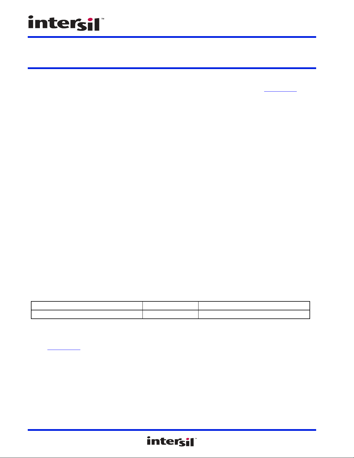
2.1 Basic Layout of the Evaluation Board
Figure 3 on page 6 shows the basic layout of the evaluation board.
Figure 4 shows the evaluation board schematic. The ISL71010BM25EV1Z contains the ISL71010BMB25Z
voltage reference (U1), input decoupling capacitors (C1, C2), a compensation capacitor (C5), and a load capacitor
(C3). Different resistor values can be applied at (R2) for testing of the voltage reference at different loads. The R2
resistor location accepts surface mount or through-hole style resistors.
The power supply leads attach to TP1 and TP2 (VIN, GND). The ISL71010B25 IC requires a DC supply in the
range of 4.0V to 30V for proper operation. The power supply should be capable of delivering 100mA of current.
The output is measured at test points TP3 and TP4 (VOUT, GND), and is best measured with a high precision voltmeter,
such as the Keysight 3458A digital multimeter, 8 1/2 digits.
The R-C damper network (R1, C4) is populated and can be connected to the reference output by adding a shunt to
the R-C jumper (J1). The damper network improves stability by reducing transient load ringing with high value
(>0.47µF) load capacitance.
2.2 Operating Range
The ISL71010B25 IC requires a VIN DC supply in the range of 4.0V to 30V for proper operation. The power
supply should be capable of delivering 100mA of current.
The ISL71010B25 IC VOUT can source 20mA of current and sink -10mA of current. For normal operation, the R2
load resistor should be selected to be ≥125Ω.
Note: With VOUT shorted to ground, the IC will limit the current to ≤75mA.
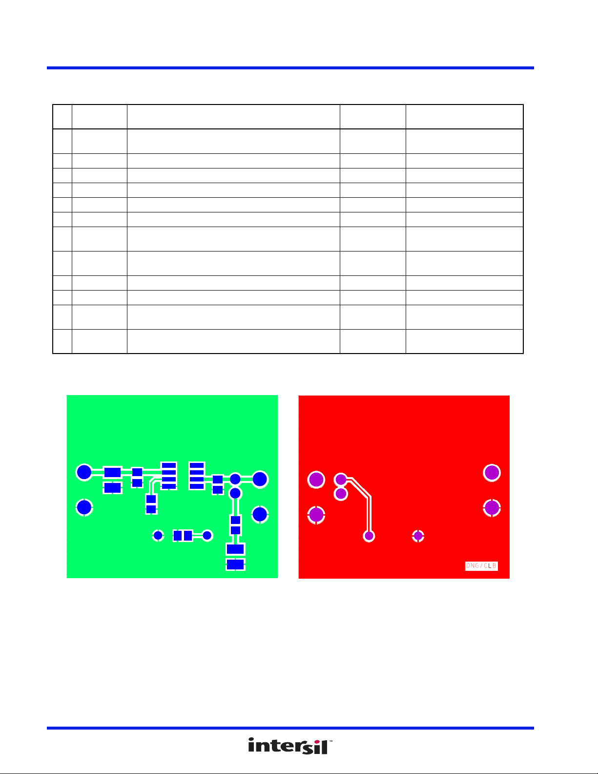
Table 1. Board Components List
Designator Value Description
C1 10µF Bypass Capacitor
C2 0.01µF Bypass Capacitor
C3 0.1µF Load Capacitor
C4 10µF Damper Capacitor
C5 1nF Compensation Capacitor
R1 2.21kΩ Damper Resistor
R2 DNP Optional Load Resistor
U1 ISL71010BMB25Z SOIC 8-Pin Package
J1 DNP Damper Jumper