User Guide 053
UG053.1
October 26, 2015
Submit Document Feedback 2
Quick Setup Guide
1. Ensure that the circuit is correctly connected to the supply and
loads prior to applying any power.
2. Connect the bias supply to VIN, the plus terminal to VIN (J1)
and the negative return to PGND (J2).
3. Connect the output load to VOUT, the plus terminal to VOUT1
(J3) and the negative return to PGND (J4).
4. Verify that the position is PWM for S1.
5. Verify the position is OPEN for S2 and S3.
6. Verify that the position is ON for S4 and S5.
7. Turn on the power supply.
8. Verify the output voltage is 1.8V for VOUT1.
Switches Control
The ISL8018 evaluation board contains S1 through S5 for various
controls of the ISL8018 circuitries. Table 1 details this function.
Frequency Control
The ISL8018 has an FS pin that controls the frequency of operation.
Programmable frequency allows for optimization between
efficiency and external component size. Default switching
frequency is 1MHz when FS is tied to VIN (R6= 0 and R5is open).
By connecting R5to GND, the switching frequency could be
changed from 500kHz (R5= 386k) to 4MHz (R5= 36k)
according to Equation 1:
When using R5to adjust the operational frequency, this also sets
external compensation mode. Please refer to the ISL8018
datasheet for more details.
Soft-Start Control
Short CSS1 to SGND for internal soft-start (approximately 1ms).
Populate CSS1 to adjust the soft-start time. This capacitor, along
with an internal 1.8µA current source, sets the soft-start interval
of the converter, tSS as shown in Equation 2.
CSS must be less than 33nF to insure proper soft-start reset after
fault condition. For proper use, do no prebias output voltage
more than regulation point.
Synchronization Control
The ISL8018 can be synchronized from 500kHz to 4MHz by an
external signal applied to the SYNCIN pin. The rising edge on the
SYNCIN triggers the rising edge of the PHASE pulse. Make sure that
the minimum on-time of the PHASE node is greater than 140ns.
SYNCOUT is a 250µA current pulse signal output triggered by the
rising edge of the clock or the SYNCIN signal (whichever is
greater in frequency) to drive the other ISL8018 and avoid the
system’s beat frequencies effects. To implement time shifting
between the master circuit to the slave, it is recommended to
add a capacitor, C13 as shown in Figure 4 of the schematic. The
time delay from SYNCOUT_Master to SYNCIN_Slave is calculated
in pF using Equation 3:
Where, t is the desired time shift between the master and the
slave circuits in ns. Care must be taken to include PCB parasitic
capacitance of ~3pF to 10pF.
The maximum should be limited to 1/Fs-100ns to insure that
SYNCOUT has enough time to discharge before the next cycle
starts.
Evaluating the Other Output Voltage
The ISL8018EVAL3Z evaluation board output is preset to 1.8V for
VOUT1, however, output voltages can be adjusted from 0.6V to
5V. The output voltage programming resistor, R1, will depend on
the desired output voltage of the regulator. The value for the
feedback resistor is typically between 0Ωand 200kΩas shown
in Equation 4.
If the output voltage desired is 0.6V, then R2is left unpopulated
and R1is shorted. For faster response performance, add 10pF to
47pF in parallel to R1, feedforward capacitor C4. Check bode plot
to insure optimum performance.
When internal compensation is used, we only need a few
external components: input capacitance, the output capacitance,
inductor, upper feedback resistor and lower feedback resistor.
Feedforward capacitor is optional. The ceramic capacitor is
recommended to be X5R or X7R.
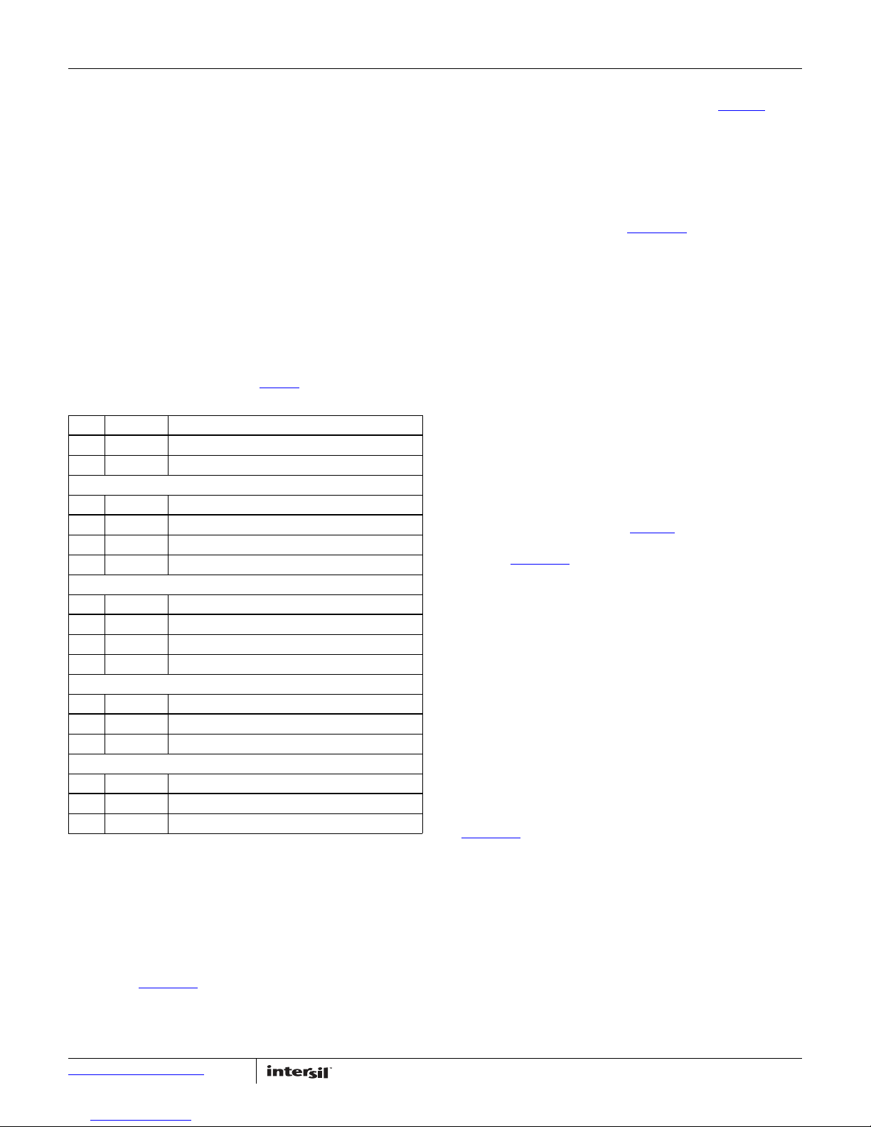
TABLE 1. SWITCH SETTINGS
S1 MODE FUNCTION
1 PWM Fixed PWM frequency at light load
3 PFM Force continuous mode
S2 ISET PROGRAM OUTPUT CURRENT
1 LOW Set output load to 3A.
- OPEN Set output load to 8A.
3 HIGH Set output load to 5A.
S3 VSET SET OUTPUT MARGIN
1 LOW Set output voltage -10%.
- OPEN No output voltage margin
3 HIGH Set output voltage +10%.
S4 ENABLE FUNCTION
1OFFDisableVOUT1
3PFMEnableVOUT1
S5 ENABLE FUNCTION
1OFFDisableVOUT2
3PFMEnableVOUT2
RTk 200 103
fOSC kHz
------------------------------ 14–= (EQ. 1)
CSS1 F 3.33 tSS s=(EQ. 2)
C13 pF 0.333 t 20–ns=(EQ. 3)
R2R1
VFB
VO VFB–
---------------------------
=(EQ. 4)


