Dual-Axis MEMS Gyro Evaluation Board
IDG-650EVB
InvenSense, Inc., 1197 Borregas, Ave. Sunnyvale, CA 94089, USA 1EB-IDG-0650-00-02
Tel: +1 (408) 988-7339 Fax: +1 (408) 988-8104 ©2009 InvenSense, Inc. All rights reserved.
Website: http//www.invensense.com
GENERAL DESCRIPTION
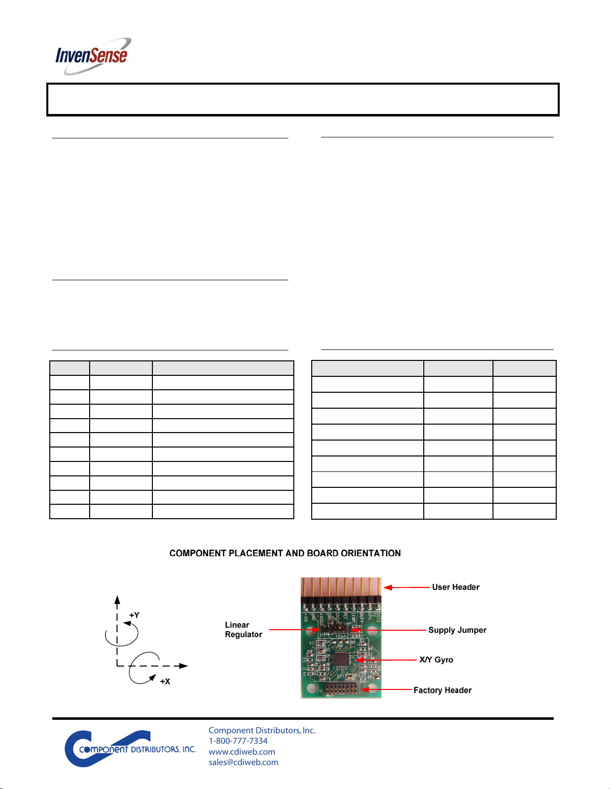
The IDG-650EVB is a fully-tested evaluation board, providing for
quick evaluation of the IDG-650 X- and Y-axis angular rate
gyroscope. The IDG-650 uses InvenSense’s proprietary MEMS
technology with vertically driven vibrating masses to produce a
functionally complete, low-cost motion sensor. All required
conditioning electronics are integrated into a single chip
measuring 4 x 5 x 1.2mm. It incorporates X- and Y-axis low-pass
filters and an EEPROM for on-chip factory calibration of the
sensor. Factory trimmed scale factors eliminate the need for
external active components and end-user calibration. A built-in
Proportional-To-Absolute-Temperature (PTAT) sensor provides
temperature compensation information. The product is lead-free
and Green Compliant.
APPLICATIONS
•High-Performance Motion Sensing Game Controllers
•Pointing Devices
•Multimedia Remotes
•Computer Mice
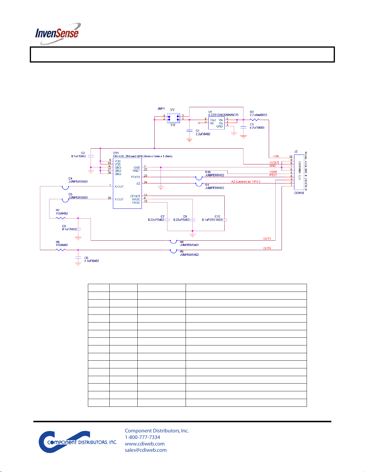
PIN DEFINITIONS
FEATURES
•Fully-tested board for easy evaluation of dual-axis gyro
•Fully integrated X- and Y-axis gyros on a single chip
•2000°/s full scale range
•0.5mV/°/s sensitivity
•Integrated amplifiers and low-pass filters
•Auto Zero function for bias calibration
•On-chip temperature sensor
•High vibration rejection over a wide frequency range
•High cross-axis isolation by proprietary MEMS design
•3V single supply operation
•Hermetically sealed for temp and humidity resistance
•10,000 gshock tolerant
•RoHS and Green Compliant
ELECTRICAL SPECIFICATIONS
Pin Signal Purpose
1 OUTX Output of the X-Axis Gyro
2 HPS Auto Zero Input
3 OUTY Output of the Y-Axis Gyro
4 TEMP Temperature Sensor Output
5 VREF Reserved for Factory Use
6 GND Ground
7 GND Ground
8 +VOUT VDD for Gyro
9 GND Ground
10 +VIN Input Supply Pin for LDO
Parameter Specifications Unit
Full-Scale Range ±2000 °/sec
Sensitivity 0.5 mV/°/sec
Cross Axis Sensitivity ± 1 %
Non-linearity < 1 % of FSR
Gyro Supply Voltage 3.0 ±0.3 V
Gyro Supply Current 7 mA
Operating Temperature -20 to +85 °C
On time 50 ms
Shock Tolerance 10,000 g
Component Distributors, Inc.
1-800-777-7334
www.cdiweb.com
sales@cdiweb.com