JETWAY NF93 Series User manual

TECHNICAL MANUAL
Of
Intel GM45 Express Chipset
&
ICH9M Chipset
Based
Mini-ITX M/B for Penyn Processor
NO.G03-NF3-F
Rev 1.0
Release date: Feb., 2009
Trademark:
* Specifications and Information contained in this documentation are furnished for information use only, and are
subject to change at any time without notice, and should not be construed as a commitment by manufacturer.

Environmental Protection Announcement
Do not dispose this electronic device into the trash while discarding. To minimize pollution
and ensure environment protection of mother earth, please recycle.
ii

TABLE OF CONTENT
USER’S NOTICE .................................................................................................................................. iii
MANUAL REVISION INFORMATION............................................................................................ iii
ITEM CHECKLIST.............................................................................................................................. iii
CHAPTER 1 INTRODUCTION OF INTELCHIPSET MOTHERBOARD
1-1 FEATURE OF MOTHERBOARD..............................................................................……1
1-2 SPECIFICATION.................................................................................................................. 2
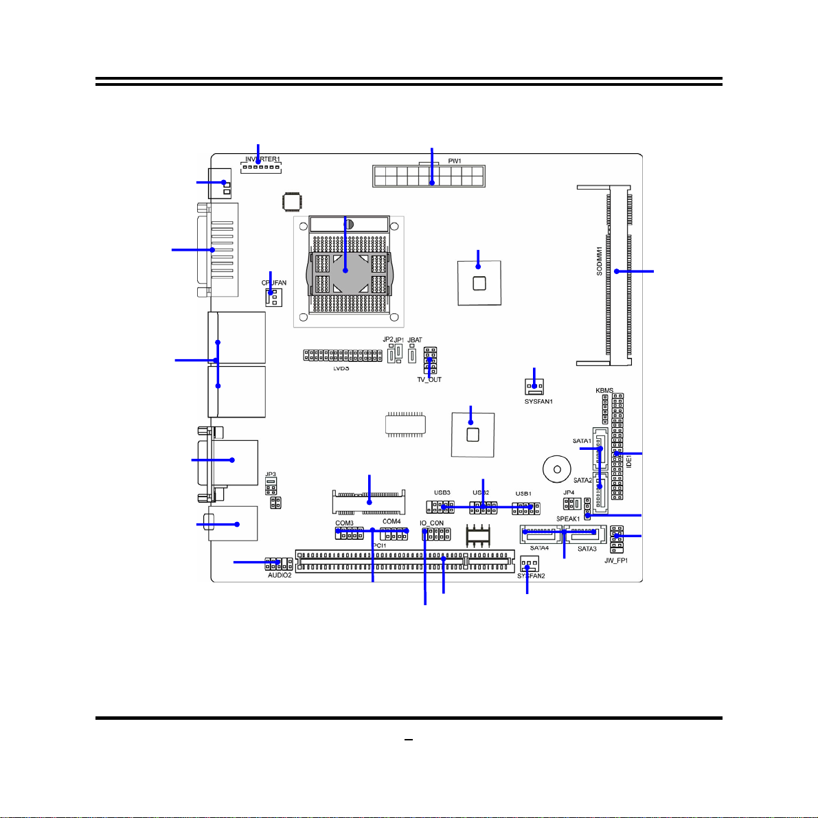
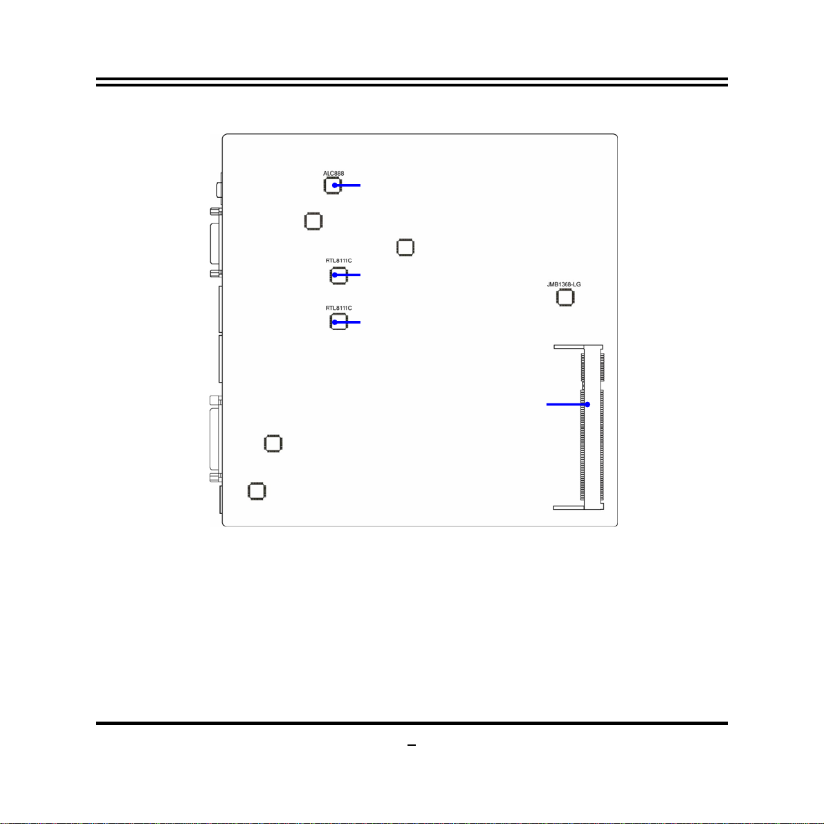
1-3 LAYOUT DIAGRAM & JUMPER SETTING................................................................... 3
CHAPTER 2 HARDWARE INSTALLATION
2-1 JUMPER SETTING..............................................................................................................7
2-2 CONNECTORS AND HEADERS ....................................................................................... 10
2-2-1 CONNECTORS....................................................................................................... 10
2-2-2 HEADERS ............................................................................................................... 11
CHAPTER 3
3-1 ENTERING SETUP…………………………………………………………………………19
3-2 GETTING HELP..…………………………………………………………………………...19
3-3 THE MAIN MENU…………………………………………………………………………..19
3-4 ADVANCED BIOS FEATURES.……………………………………………………………22
3-4-1 CPU FEATURE………………………………………………………………………………25
3-5 INTERGRATED PERIPHERALS…….................................................................................25
3-5-1 INTEL DTS FEATURE………………………………………………………………………26
3-6 PC HEALTH STATUS………………………………………………………………………28
3-7 ADVANCED CHIPSET FEATURES……………………………………………………….29
3-8 POWER MANAGEMENT SETTING..………………………………………...…….……..30
3-9 PnP/PCI CONFIGURATION………………………………………………………………...32
iii

Safety Environmental Instruction
zAvoid the dusty, humidity and temperature extremes. Do not place the product in any
area where it may become wet.
z0 to 60 centigrade is the suitable temperature. (The figure comes from the request of the
main chipset)
zGenerally speaking, dramatic changes in temperature may lead to contact malfunction
and crackles due to constant thermal expansion and contraction from the welding spots’
that connect components and PCB. Computer should go through an adaptive phase
before it boots when it is moved from a cold environment to a warmer one to avoid
condensation phenomenon. These water drops attached on PCB or the surface of the
components can bring about phenomena as minor as computer instability resulted from
corrosion and oxidation from components and PCB or as major as short circuit that can
burn the components. Suggest starting the computer until the temperature goes up.
zThe increasing temperature of the capacitor may decrease the life of computer. Using the
close case may decrease the life of other device because the higher temperature in the
inner of the case.
zAttention to the heat sink when you over-clocking. The higher temperature may decrease
the life of the device and burned the capacitor.
iv

v
USER’S NOTICE
COPYRIGHT OF THIS MANUAL BELONGS TO THE MANUFACTURER. NO PART OF THIS MANUAL,
INCLUDING THE PRODUCTS AND SOFTWARE DESCRIBED IN IT MAY BE REPRODUCED,
TRANSMITTED OR TRANSLATED INTO ANY LANGUAGE IN ANY FORM OR BY ANY MEANS WITHOUT
WRITTEN PERMISSION OF THE MANUFACTURER.
THIS MANUAL CONTAINS ALL INFORMATION REQUIRED TO USE INTEL GM45 CHIPSET
MOTHER-BOARD SERIES AND WE DO ASSURE THIS MANUAL MEETS USER’S REQUIREMENT BUT WILL
CHANGE, CORRECT ANY TIME WITHOUT NOTICE. MANUFACTURER PROVIDES THIS MANUAL “AS IS”
WITHOUT WARRANTY OF ANY KIND, AND WILL NOT BE LIABLE FOR ANY INDIRECT, SPECIAL,
INCIDENTIALORCONSEQUENTIAL DAMAGES (INCLUDING DAMANGES FOR LOSS OF PROFIT, LOSS OF
BUSINESS, LOSS OF USE OF DATA, INTERRUPTION OF BUSINESS AND THE LIKE).
PRODUCTS AND CORPORATE NAMES APPEARING IN THIS MANUAL MAY OR MAY NOT BE
REGISTERED TRADEMARKS OR COPYRIGHTS OF THEIR RESPECTIVE COMPANIES, AND THEY ARE
USED ONLY FOR IDENTIFICATION OR EXPLANATION AND TO THE OWNER’S BENEFIT, WITHOUT
INTENT TO INFRINGE.
Manual Revision Information
Reversion Revision History Date
1.0 First Edition February, 2009
Item Checklist
5Motherboard
5Cable(s)
5CD for motherboard utilities
5Motherboard User’s Manual
5Back panel

1
Chapter 1
Introduction of the Motherboard
1-1 Feature of motherboard
zIntel GM45+ICH9M chipset.
zPenyn CPU, with low power consumption never denies high performance.
zSupport FSB 1066MHz
zSupport two DDRII SODIMM 800/667MHz up to 4 GB.
zOnboard two REALTEK RTL 8111C Gigabit Ethernet LAN.
zIntegrated ALC888 6-channel HD audio CODEC.
zSupport USB2.0 data transport demands.
zSupport RS422/485 and watchdog.
zSupport GPIO function.

2
1-2 Specification
Spec Description
Design ∗Mini ITX form factor 8 layers PCB size: 17.0x17.0cm
Chipset ∗Intel GM45+ICH9M Chipset
CPU ∗Penyn CPU
Memory Socket
∗200-pin DDRII SO-DIMM socket x2
∗Support DDRII SODIMM 800/667 MHz system Modules DDRII
SODIMM memory
∗Expandable to 4GB.
x
Expansion Slots ∗32-bit PCI slot x 1pcs
∗Mini PCI-E x1pcs
Integrate IDE ∗One PCI IDE controller that supports PCI Bus Mastering, ATA
PIO/DMA and the ULTRA DMA 100/66 functions that deliver
the data transfer rate up to 100 MB/s.
LAN
∗Integrated two Realtek RTL8111C PCI-E Gigabit LAN.
∗Support Fast Ethernet LAN function of providing
10Mb/100Mb/1000Mb Ethernet data transfer rate
Audio ∗ALC888 6 channel Audio Codec integrated
∗Audio driver and utility included
BIOS ∗Award 8MB Flash DIP ROM
Multi I/O ∗Hard disk drive connector x1
∗SATAII x4
∗USB2.0 port x 4 and headers x6
∗RJ45 LAN connector x2
∗Audio connector x1 (Line-in, Line-out, MIC,SPDIF_OUT)
∗COM connector x 2
∗COM Header x2

∗LVDS Connector x1
∗VGA Connector x1
∗DVI-D Connector x1
∗TV OUT x1
∗HDMI Connector x1
1-3 Layout Diagram & Jumper Setting
DVI-D
Connector
3
COM
nnector
Co
RJ45 LAN
RJ45 LAN
Line-Out
Line-In/
SPDIF Out
MIC-IN
HDMI
Connector VGA
Connector USB
Connector USB
Connector COM
Connector

Inverter Connector
4
ATX Power Connector
HDMI Connector
Intel Penyn
VGA & DVI-D
Connector
SYS FAN1
TV OUT Connector
Intel GM45 Chipset
Intel ICH9M Chipset
DDRII
SO-DIMM
CPU FAN
USB Connector
IDE Connecto
r
Speaker connecto
r
USB Connector
SATAII Connector (1,2)
COM Connector
Mini PCI-E Slot
Audio Connector Front Panel Connector
PCI Slot
GPIO Connector
Front Panel Audio
SYS FAN2
SATAII Connector 3,4)
COM Connector

ALC 888
RealtekRTL8111C
Gi
g
abit Lan
RealtekRTL8111C
Gi
g
abit Lan
DDRII
SO-DIMM
5

6
Jumper
Jumper Name Description Page
JP1 Panel backlight selecting 3-pin Block P.8
JBAT CMOS RAM Clear Function Setting 3-pin Block P.8
JP2 Panel VDD Select 3-pin Block P.9
JP3 RS232/422/485 Function Select 6-pin Block P.9
JP4 Powered RS232 Select 6-pin Block P.10
Connectors
Connector Name Description Page
USB USB Port Connector 4-pin Connector P.10
UL2 RJ45 LAN Connector RJ-45 Connector P.10
VGA Video Graphic Attach Connector D-sub15-pin Female P.10
AUDIO1 Line-Out /MIC/Line-In Audio Connector 3 Phone Jack P.10
COM1,2 Serial Port COM1 Connector 9-pin Connector P.10
DVI-D Connector DVI port connector 24-pin Connector P.10
HDMI Connector HDMI port connector 19-pin Connector P.10

7
HeadersHeader Name Description Page
CPUFAN,SYSFAN1/2 FAN Speed Headers 3-pin Block P.15
AUDIO1 Front panel audio Headers 9-pin block P.11
TV Out1 TV Out Header 9-pin block P.14
PWR LED Power LED 4-pin Block P.15
LVDS LVDS Connector 32-pin Block P.12
Inverter LVDS Inverter Connector 7-pin Block P.13
COM3,4 Serial Port COM3/4 Connector 9-pin Connector P.16
JW_FP
(PWR LED/ HD LED/ /Power
Button /Reset)
Front Panel Header
(PWR LED/ HD LED/ /Power Button
/Reset)
9-pin Block P.15
SATA1~4 Serial ATAII IDE Connector 7-pin Connector P.11
GPIO GPIO header 10-pin Connector P.16
KBMS Header PS/2 Keyboard and mouse connector 6-pin Connector P.17

Chapter 2
2-1 Jumper Setting
(1) Clear CMOS (3-pin): JBAT
CMOS RAM Clear Setting
2-3 closed Clear CMOS
JBAT JBAT
1-2 closed Normal
3
1
3
1
(2) JP1: Panel backlights select (3-pin)
8
1-2 closed Off
2-3 closed On
JP1
JP1
3
1
3
1

(3) JP2: Panel VDD Select (3-pin)
JP2
1-2 closed: 5V
2-3 closed : 3.3V
3
1
3
1
JP2
(4) JP3: Power RS232/422/485 Function Select
JP3
1-2 closed: RS23
3-4 closed : RS485
1
2
1
5-6 closed : RS422
1
9

(5) JP4: Powered RS232 Select :
JP4
1-2 closed: R
10
2-2 Connectors and Headers
2-2-1 Connectors
(1) Audio Connector: (Line-IN/ Line-Out/ MIC-In)
3-4 closed : +12V
1
S232
1
5-6 closed : +5V
1
VGA
Connector
COM
Connector
RJ45 LAN
USB
Connector USB
Connector
DVI
Connector COM
onnector
C
RJ45 LAN
Line-In/
SPDIF Out
Line-Out
HDMI
Connector
MIC-In

(2) Serial-ATA Port connector: SATA1/SATA2/ SATA3/SATA4
Serial-ATA Co
SATA4
SATA2
SATA1
11
2-2-2 Headers
(1) Front panel audio (9-pin): AUDIO1
nnectors
SATA3
Line-Out, MIC Headers
AUDIO1
Pin 1
MIC2-L
LINE OUT2-L
MIC2-R
LINE OUT2-R
SENSE-FB
GND
Line2-JD
MIC2-JD
NC
2
9
10

12
(2) LVDS Headers: LVDS
Pin NO. Pin Define Pin NO. Pin Define
Pin 1 NC Pin 2 NC
Pin 3 LVDS_CLKBN Pin 4 LVDS_CLKBP
Pin 5 LVDSA_DATAN2 Pin 6 LVDSA_DATAP2
Pin 7 LVDSA_DATAN1 Pin 8 LVDSA_DATAP1
Pin 9 LVDSA_DATAN0 Pin 10 LVDSA_DATAP0
Pin 11 LVDS_DDC_DATA Pin 12 LVDS_DDC_CLK
Pin 13 GND Pin 14 GND
Pin 15 GND Pin 16 GND
Pin 17 NC Pin 18 NC
Pin 19 LVDS_CLKAP Pin 20 LVDS_CLKAN
Pin 21 LVDSB_DATAP2 Pin 22 LVDSB_DATAN2
Pin 23 LVDSB_DATAP1 Pin 24 LVDSB_DATAN1
Pin 25 LVDSB_DATAP0 Pin 26 LVDSB_DATAN0
Pin 27 PVDD Pin 28 PVDD
Pin 29 PVDD Pin 30 PVDD
Pin 31 GND Pin 32 GND

Pin 1
13
LVDSHeader
Pin 2
(3) Pin-headers of LVDS Inverter:
Pin 1 and pin2: VCC of inverter
Pin3、pin4 and pin6: GND
Pin5: Backlight
Pin7: Brightness
VCC
VIN
GND
GND
GND
Backlight
Brightness
Pin 1

(4) TV-OUT Header:
TV-OUT Header
GND
NC
NC
GND
Blue
TV-OUT
Pin1
2
9
10
Green
Red
Key
NC
NC
(6) RS422/485 Header:
14
RS422/485 Header
TX-RXCOM4 Pin1
TXDN
RXDN
TXDP
2
RXDP

(7) JW-FP(9-pin)
System Case Connections
HDLED
RESET
VCC5
GND
VCC5 PWR LED
PWRBTN
PWRBTN
PWRLED
HDDLE
RSTSW
NC GND
JW FP
Pin 1
SPEAK
SPKR
GND
NC
VCC5
Pin 1
(8) FAN Speed Headers (3-pin): CPUFAN, SFAN1/SFAN2
SYSFAN1
CPUFAN
SYSFAN2
Pin1
Pin1
Pin1
15
Table of contents
Other JETWAY Motherboard manuals

JETWAY
JETWAY A210GDMS - REV 1.0 User manual

JETWAY
JETWAY NC8J Series User manual

JETWAY
JETWAY S446R2A User manual

JETWAY
JETWAY 754TURBOR208 User manual

JETWAY
JETWAY 865GF User manual

JETWAY
JETWAY XBLUE-78VA2 User manual

JETWAY
JETWAY J7F4-F User manual

JETWAY
JETWAY S450R2A User manual

JETWAY
JETWAY I405R4A User manual

JETWAY
JETWAY 917PDCPR106 User manual

JETWAY
JETWAY P4MDFTR1A User manual

JETWAY
JETWAY NU95 Series User manual

JETWAY
JETWAY Kocab 18G User manual

JETWAY
JETWAY NF731 User manual

JETWAY
JETWAY NC9T User manual

JETWAY
JETWAY 848PDAR1A User manual

JETWAY
JETWAY V333DAR2A User manual

JETWAY
JETWAY K8M8MSR1A User manual

JETWAY
JETWAY V880DASR2A User manual

JETWAY
JETWAY G03-NC94-F User manual