JVC PD-42DX6BJ User manual

SERVICE MANUAL
COPYRIGHT © 2005 Victor Company of Japan, Limited No.YA295
2005/5
PDP INTEGRATED DIGITAL TV
YA29520055
PD-42DX6BJ,
PD-42DX6BJ/P
TABLE OF CONTENTS
1 PRECAUTION. . . . . . . . . . . . . . . . . . . . . . . . . . . . . . . . . . . . . . . . . . . . . . . . . . . . . . . . . . . . . . . . . . . . . . . . . 1-3
2 SPECIFIC SERVICE INSTRUCTIONS . . . . . . . . . . . . . . . . . . . . . . . . . . . . . . . . . . . . . . . . . . . . . . . . . . . . . . 1-6
3 DISASSEMBLY . . . . . . . . . . . . . . . . . . . . . . . . . . . . . . . . . . . . . . . . . . . . . . . . . . . . . . . . . . . . . . . . . . . . . . 1-11
4 ADJUSTMENT . . . . . . . . . . . . . . . . . . . . . . . . . . . . . . . . . . . . . . . . . . . . . . . . . . . . . . . . . . . . . . . . . . . . . . . 1-23
5 TROUBLESHOOTING . . . . . . . . . . . . . . . . . . . . . . . . . . . . . . . . . . . . . . . . . . . . . . . . . . . . . . . . . . . . . . . . . 1-31
BASIC CHASSIS
FP3

1-2 (No.YA295)
SPECIFICATION
Design & specifications are subject to change without notice.
Items Contents
Dimensions ( W ×H ×D )
104.5 cm
×
79.5 cm
×
31.3 cm [Included stand]
104.5 cm
×
72.8 cm
×
11.0 cm [TV only]
Mass 45 kg [Included stand]
38.5 kg [TV only]
TV RF System Analog
Digital
CCIR (I)
DVB-T
Colour System PAL / NTSC 3.58/4.43 [EXT only]
Stereo System NICAM (I)
Receiving
Frequency
Analog
Digital
UHF: 470 MHz - 862 MHz
UHF: 474 MHz - 850 MHz
Intermediate
Frequency
VIF
SIF
38.9 MHz (I)
32.9 MHz (6.0MHz :I)
Colour Sub
Carrier Frequency
PAL
NTSC
4.43 MHz
3.58 MHz / 4.43 MHz
Teletext System Analog
Digital
FLOF (Fastext level 2.5), WST(World Standard system)
MHEG 5 UK profile
Power Input AC110 V - AC240 V, 50 Hz / 60 Hz
Power Consumption 170 W (Standby: 2.6 W)
TV RF System Analog
Digital
CCIR (I)
DVB-T
Power Input AC110V - AC240 V, 50 Hz / 60 Hz
Power Consumption Operate: 339 W, Stand by: 3.0 W
Plasma Display Panel (PDP) 42V wide aspect (16 : 9)
Screen Size Diagonal : 106 cm (H:91.8 cm ×V : 51.8 cm)
Display Pixels Horizontal : 1024 dots ×Vertical : 768 dots (XGA)
Audio Power Output 10 W + 10 W
Speaker 6.6 cm round ×4 (Obligue cone)
EXT-1 / EXT-2 / EXT-3 (Input / Output) 21-pin Euro connector (SCART socket ) ×3
EXT-4 (Input) Component Video
1125i
625p / 525p / 625i / 525i
Video
Audio
RCA pin jack ×3
Y : 1V (p-p) (Sync signal: ±0.35V(p-p), 3-value sync.), 75Ω
Pb/Pr : ±0.35V(p-p), 75 Ω
Y : 1V (p-p), Positive (Negative sync provided), 75 Ω
Cb/Cr : 0.7V(p-p), 75 Ω
1V (p-p), Positive (Negative sync provided), 75 Ω, RCA pin jack ×1
500mV(rms) (-4dBs), high impedance, RCA pin jack ×2
EXT-5 (Input) S-Video
Video
Audio
Mini-DIN 4 pin ×1
Y: 1V (p-p), Positive (Negative sync provided), 75 Ω
C: 0.286V (p-p) (Burst signal), 75 Ω
1V (p-p), Positive (Negative sync provided), 75 Ω, RCA pin jack ×1
500mV (rms), High impedance, RCA pin jack ×2
HDMI Input Video
Audio
HDMI connector ×1
(Digital-input terminal is not compatible with picture signals of computer signal)
Digital: HDMI connector ×1
Anarog: 500mV(rms) (-4dBs), high impedance, RCA pin jack ×2
PC (RGB) Input D-sub 15pin ×1
R/G/B : 0.7V (p-p), 75Ω
HD / VD : 1V (p-p) to 5V (p-p), high impedance
< Available signal >
VGA : 640 pixels ×480 pixels (Horizontal : 31.5kHz / Vertical : 60Hz)
XGA : 1024 pixels ×768 pixels (Horizontal : 42.0kHz / Vertical : 60Hz)
Centre Channel Input 500 mV(rms) (-4dBs), high impedance,RCA pin jack ×1
Audio Output 500 mV (rms), Low impedance, RCA pin jack ×2
Subwoofer Output
More than 0 to 1000 mV (rms) (+2.2dBs), low impedance (80Hz when modulated 100%), RCA pin jack
×
1
Headphone 3.5 mm stereo mini jack ×1
Remote Control Unit RM-C1813H (AA/R6 dry cell battery ×2)

(No.YA295)1-3
SECTION 1
PRECAUTION
1.1 SAFETY PRECAUTIONS
(1) The design of this product contains special hardware and many circuits and components specially for safety purposes. For
continued protection, no changes should be made to the original design unless authorized in writing by the manufacturer.
Replacement parts must be identical to those used in the original circuits. Service should be performed by qualified personnel
only.
(2) Alterations of the design or circuitry of the product should not be made. Any design alterations or additions will void the
manufacturer's warranty and will further relieve the manufacturer of responsibility for personal injury or property damage
resulting therefrom.
(3) Many electrical and mechanical parts in the product have special safety-related characteristics. These characteristics are often
not evident from visual inspection nor can the protection afforded by them necessary be obtained by using replacement
components rated for higher voltage, wattage, etc. Replacement parts which have these special safety characteristics are
identified in the Parts List of Service Manual. Electrical components having such features are identified by shading on the
schematics and by ( ) on the Parts List in the Service Manual. The use of a substitute replacement which does not have the
same safety characteristics as the recommended replacement part shown in the Parts List of Service Manual may cause shock,
fire, or other hazards.
(4) The leads in the products are routed and dressed with ties, clamps, tubing’s, barriers and the like to be separated from live parts,
high temperature parts, moving parts and / or sharp edges for the prevention of electric shock and fire hazard. When service is
required, the original lead routing and dress should be observed, and it should be confirmed that they have been returned to
normal, after re-assembling.
WARNING
(1) The equipment has been designed and manufactured to meet international safety standards.
(2) It is the legal responsibility of the repairer to ensure that these safety standards are maintained.
(3) Repairs must be made in accordance with the relevant safety standards.
(4) It is essential that safety critical components are replaced by approved parts.
(5) If mains voltage selector is provided, check setting for local voltage.

1-4 (No.YA295)
1.2 INSTALLATION
1.2.1 HEAT DISSIPATION
If the heat dissipation vent behind this unit is blocked, cooling efficiency may deteriorate and temperature inside the unit will rise. The
temperature sensor that protects the unit will be activated when internal temperature exceeds the pre-determined level and power will
be turned off automatically.
Therefore, please make sure pay attention not to block the heat dissipation vent as well as the ventilation outlet behind the unit and
ensure that there is room for ventilation around it.
1.2.2 INSTALLATION REQUIREMENTS
Ensure that the minimal distance is maintained, as specified below, between the unit with and the surrounding walls, as well as the
floor etc. Install the unit on stable flooring or stands. Take precautionary measures to prevent the unit from tipping in order to protect
against accidents and earthquakes.
SPACE REQUIRED FOR INSTALLATION
1.2.3 FALL TIP PREVENTION MEASURES
Take precautionary measures to prevent the unit from falling or
tipping, and to protect against emergencies such as earthquakes
as well as accidents.
Fasten the fall tip prevention hooks on the back of the display
with the screws, and secure the unit to a robust part such as the
wall surface or pillars with durable cords.
NOTE:
The hooks and screws are not supplied with this model.
200 mm 200 mm
50 mm
50 mm
150 mm
150 mm
200 mm or
more
200 mm
or more
50 mm or more
50 mm or more
150 mm
or more
150 mm or
more
The hooks for tip/fall prevention

(No.YA295)1-5
1.3 PRECAUTIONS REGARDING PDP
1.3.1 PRECAUTIONS DURING NOTES FOR TRANSPORTATION
When transporting the unit, pressure exerted on the internal PDP
(Plasma Display Panel) due to improper handling (such as
tossing and dropping) may cause damages even when the unit
is carefully packed. To prevent accidents from occurring during
transportation, pay careful attention prior to delivery such as
through explaining the handling instructions to transporters.
Ensure that the following requirements are met during
transportation, as the PDP of this unit is made of glass and
therefore fragile:
(1) Avoid vibrations and impacts
The unit may be broken if it is toppled sideways even when
properly packed. Ensure that the unit is carried by at least
2 persons and pay careful attention not to exert any
vibration or impact on it.
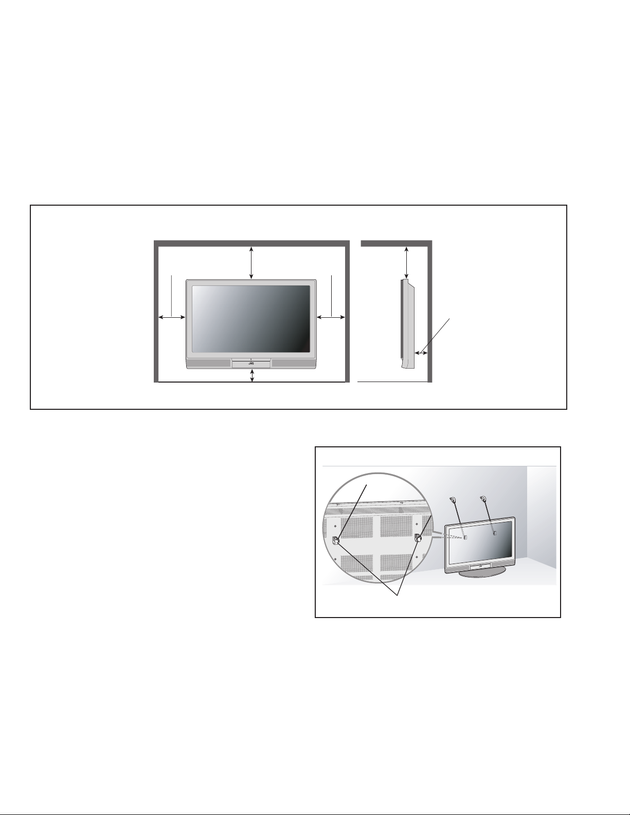
(2) Do not place equipment horizontally
Ensure that it is placed upright and not horizontally during
transportation and storage as the PDP is very vulnerable to
lateral impacts and may break easily under such
circumstances.
During transportation, ensure that the unit is loaded along
the traveling direction of travel of the vehicle, and avoid
stacking them on one another.
For storage, ensure that they are stacked in 2 layers or less
even when placed upright.
1.3.2 RESIDUAL IMAGE / BURN-IN ON SCREEN
Like CRTs, "burn-in" may occur when a same image is
continuously displayed over an extended period of time.
As this may also shorten the life span of the PDP. Therefore, turn
off the display when not in use, scroll the screen, make use of
screen-savers, or allow even distribution on the display by
inverting the brightness, switching to complementary colors or
inserting animated images at periodic intervals.
As burn-in is more likely to occur with high brightness and
contrast settings, try to use neutral gradations or medium tone
colors.
Burn-in does not occur in the case of animated images.
When switching to another image after continuous display of the
previous image, residual images may become prominent, as
luminance in a part of the display is higher than the other parts.
This is not a defect but is because due to the discharge surface
of the lighted portion has become being relatively activated and
its luminance higher than the unlighted parts.
1.3.3 INFRARED RAYS
Near Near-infrared rays (800nm to 1000nm) are emitted from the
front of the panel, and this may give rise to malfunctions in
infrared remote controls or communication systems placed near
it. In this case, avoid direct infrared rays (and reflected rays in
some cases) from the screen by either changing the direction of
the unit or other infrared systems or securing a longer keeping a
distance from the screen.
1.3.4 OPTICAL FILTER (PANEL FILTER)
Avoid placing the unit under direct sunlight over a prolonged
period of time. This may cause the optical filter to deteriorate in
quality and color.
Clean the filter surface by wiping it softly lightly with outing
flannels a soft and lightly fuzz cloth (such as flannel).
Do not use solvents such as benzine or thinner to wipe the filter
surface. This may cause the filter to deteriorate in quality or the
coating on the surface to come off.
As the filter surface is fragile., do not scratch or hit it with hard
materials.
1.3.5 NOTES PRECAUTIONS FOR PEPLACEMENT OF
EXTERIOR PARTS
Take note of the following when replacing exterior parts (back
REAR COVER, FRONT PANEL, optical filter)
• Do not exert pressure on the front of the PDP (glass surface).
• Pay careful attention not to scratch or stain the front of the PDP
(surface) with hands.
• When replacing exterior parts, the front of the PDP should be
placed facing downward. Place a mat, etc. underneath to avoid
causing scratches to the front surface. However, never use
materials that are too soft (such as blanket cloth). If
replacement is made with the PDP surface facing downward
and in contact with the blanket, pressure may be exerted on
the PDP, thus causing damages to it.

1-6 (No.YA295)
SECTION 2
SPECIFIC SERVICE INSTRUCTIONS
2.1 SYSTEM SETTEING
(1) Press the [INFORMATION] key and [MUTING] key
simultaneously, then enter the SERVICE MODE.
(2) When the Main Menu is displayed, press [2] key to enter
the self check mode.
(3) Turn off the power by pressing the [POWER] key on the
remote control unit.
2.2 FEATURES
DVB-T (DIGITAL TERRESTRIAL BROADCASTING)
This TV can receive both Digital terrestrial broadcasting (DVB-
T) and Analogue terrestrial broadcasting.
D.I.S.T. (Digital Image Scaling Technology)
This system uses line interpolation to double the number of
scanning lines and achieve high resolution, flicker-free picture.
COLOUR MANAGEMENT
This function ensures dull colours are compensated to
produce natural hues.
PICTURE MANAGEMENT
This function makes it easier to see the dark areas when a
picture has many dark areas, and makes it easier to see the
bright areas when a picture has many bright areas.
ZOOM
This function can change the screen size according to the
picture aspect ratio.
DIGITAL VNR
This function cuts down the amount of noise in the original
picture.
SUPER DIGIPURE
This function uses the latest in digital technology to give you a
natural-looking picture.
MOVIE THEATRE
This function displays a cinema film picture more smoothly and
naturally on the screen.
3D CINEMA SOUND
You can enjoy sounds with a widerambience.
DIGITAL INPUT
Digital-in will display when any picture signal (480i/ 480p,
720p/ 1080i) in Digital-in is displayed.
BBE
High definition audio adds natural, clear and extraordinary
sound quality to any program.
Be sure to carry out the following operation at the end of
the procedure.
MAIN MENU SCREEN
SELF CHECK MODE SCREEN
LOB OK FAN OK
LOB OK FAN OK
SYNC M:OK S:OK HD:NG
TIM OK
TIM OK
MSM OK DIGI 0000
MSM OK DIGI 0000
MEM OK AVSW OK
MEM OK AVSW OK
YC OK AIO OK
YC OK AIO OK
TUN OK GCR NG 1
TUN OK GCR NG 1
IP OK RGB OK 8
IP OK RGB OK 8
DVI OK HDMI OK
DVI OK HDMI OK
SERVICE MENU
SERVICE MENU
1.ADJUST
1.ADJUST
2.SELF_CHK
2.SELF_CHK
3.I2C STOP
3.I2C STOP

(No.YA295)1-7
2.3 HOW TO IDENTIFY MODELS
2.4 21-PIN EURO CONNECTOR (SCART) : EXT-1 / EXT-2 / EXT-3
(P-P= Peak to Peak, B-W= Blanking to white peak)
"AE" or "PE" are added to the serial No. under at the Rating label.
Pin
No.
Signal designation Matching value EXT-1 EXT-2 EXT-3
1 AUDIO R output 500mV(rms) (Nominal), Low impedance Used (TV OUT) Used (LINE OUT) Not used
2 AUDIO R input 500mV(rms) (Nominal), High impedance Used (R1) Used (R2) Used
3 AUDIO L output 500mV(rms) (Nominal), Low impedance Used (TV OUT) Used (LINE OUT) Not used
4 AUDIO GND Used Used Used
5 GND (B) Used Used Used
6 AUDIO L input 500mV(rms) (Nominal), High impedance Used (L1) Used (L2) Used
7 B input 700mV(B-W), 75ΩUsed Used Not used
8 FUNCTION SW
(SLOW SW)
Low : 0V-3V High : 8V-12V, High impedance
Used Used Used
9 GND (G) Used Used Used
10 SCL / T-V LINK Not used
Used(SCL2 / TV-LINK)
Not used
11 G input 700mV(B-W), 75ΩUsed Used Not used
12 SDA Not used Used (SDA2) Not used
13 GND (R) Used Used Used
14 GND (YS) Used Not used Not used
15 R / C input R : 700mV(B-W), 75ΩC : 300mV(P-P), 75ΩUsed (R) Used (C2/R) Not used
16 Ys input (FAST SW) Low : 0V-0.4V, High : 1V-3V, 75ΩUsed Used Used
17 GND (VIDEO output) Used Used Used
18 GND (VIDEO input) Used Used Used
19 VIDEO output 1V(P-P) (Negative sync), 75ΩUsed (TV OUT) Used (LINE OUT) Not used
20 VIDEO / Y input 1V(P-P) (Negative sync), 75ΩUsed Used Used
21 COMMON GND Used Used Used
Indicated
AE
PE
MODEL No.
SERIAL NO.
NUMERO DE SERIE
PD-42DS6BJ
20 18 16 14 12 10 8 6 4 2
21 19 17 15 13 11 9 7 5 3 1
[Pin assignment]

1-8 (No.YA295)
2.5 TECHNICAL INFORMATION
2.5.1 PDP STRUCTURE AND CHARACTERISTIC
This unit uses the flat type panel PDP (Plasma Display Panel), instead of the conventional CRT (Cathode Ray Tube), as a display unit.
2.5.1.1 PIXEL (CELL) ARRAY
PDP is constructed by sealing the xenon, which emits neon and ultraviolet rays for discharging purpose, in between the electrodes
lay on the front glass substrate and rear glass substrate.
One pixel is composed of 3 RGB cells, with cell pitch of 0.304mm (1 pixel 0.912mm) horizontally and 0.693mm vertically.
The cell is arrayed in each RGB color as shown in Fig. 1. One pixel is formed by interlacing each RGB color cell.
One cell size is 0.299mm horizontally and 0.693mm vertically.
Fig.1
2.5.1.2 PIXEL DEFECTS
Though PDP is made by means of ultra precise technology, there are cases whereby not all pixels (cell) will function properly. In some
cases, there may be defective pixels that do not light at all or the ones that always light on.
There are 3 types of Pixel defects, [Bright Dot Defects], [Dark Dot Defects] and [Flicker Dot Defects], as defined respectively in the
following:
(1) BRIGHT FAULT
In this pixel fault, a cell that should not light originally is lighting on and off.
For checking this pixel fault, input ALL BLACK SCREEN and find out the cell that is lighting on and off.
(2) DARK FAULT
In this pixel fault, a cell that should light originally is not lighting or lighting with the brightness twice as brighter as originally lighting.
For checking this pixel fault, input 100% of each R/G/B colour and find out the cell that is not lighting.
(3) FLICKER FAULT
In the pixel fault, a cell that should light originally or not light originally is flashing on and off.
For checking this pixel fault, input ALL BLACK SCREEN signal or 100% of each RGB colour and find out the cell that is flashing on
and off.
B G R B G R
BGRBGR
GRBG R
GRBGR
B
B
BGRBG R
BGRBGR
GRBG R
GRBGR
B
B
No.1
Pixel
sequence
No.2
Pixel
sequence Pixel
sequence
No.1023 No.1024
0.693mm (Vertically)
Pixel
sequence
No.1
Pixel line
No.2
Pixel line
Horizontally
Vertically
Direction
0.912mm
(Horizontally) Pixel pitch
0.304mm
(Horizontally) Cell pitch
Pixel pitch (Cell pitch)
1 pixel
(1 dot)
No.767
Pixel line
No.768
Pixel line
B Cell
G
Cell
R Cell

(No.YA295)1-9
2.5.2 MAIN CPU PIN FUNCTION [IC7501 : DIGITAL SIGNAL PWB ASS'Y]
Pin Pin name I/O Function Pin Pin name I/O Function
1 TCK I Test purpose 65 D2 I/O Program ROM data for main CPU
2 TMS I Test purpose 66 D12 I/O Program ROM data for main CPU
3 TDI I Test purpose 67 D10 I/O Program ROM data for main CPU
4 TDO O Test purpose 68 VSS33 - GND
5 P2.8 O Not used 69 VDD33 I 3.3V
6 P2.9 O Blue for OSD 70 D4 I/O Program ROM data for main CPU
7 P2.10 O Blue for OSD 71 D3 I/O Program ROM data for main CPU
8 P2.11 O Blue for OSD 72 D11 I/O Program ROM data for main CPU
9 P2.12 O Blue for OSD 73 RSTIN I Reset
10 P2.13 O Blue for OSD 74 POWER O Sleep state release for chassis CPU [Relese : L]
11 P2.14 I Not used 75 P3.1 O Not used
12 P2.15 O Request for chassis CPU communication 76 REMOCON I Remote control
13 VSS33 - GND 77 P3.3 I Clock for OSD
14 VDD33 I 3.3V 78 P3.4 O Red for OSD
15 P4.5 O Not used 79 P3.5 O Red for OSD
16 A20 O Program ROM address for main CPU 80 P3.6 O Red for OSD
17 A19 O Program ROM address for main CPU 81 P3.7 O Red for OSD
18 A18 O Program ROM address for main CPU 82 MTST O Data transmission for chassis CPU communication
19 A17 O Program ROM address for main CPU 83 MTSR I Data receive for chassis CPU communication
20 VSS25 - GND 84 VSS33 - GND
21 VDD25 I 2.5V 85 VDD33 I 3.3V
22 A16 O Program ROM address for main CPU 86 VSS25 - GND
23 A8 O Program ROM address for main CPU 87 VDD25 I 2.5V
24 A7 O Program ROM address for main CPU 88 TXD0 O Communication for adjustment
25 A9 O Program ROM address for main CPU 89 RXD0 O Communication for adjustment
26 A6 O Program ROM address for main CPU 90 P3.12 O Red for OSD
27 A5 O Program ROM address for main CPU 91 CLK O Clock for chassis CPU communication
28 A10 O Program ROM address for main CPU 92 P3.15 O Green for OSD
29 A11 O Program ROM address for main CPU 93 P5.14 O Green for OSD
30 A12 O Program ROM address for main CPU 94 P5.15 O Green for OSD
31 VSS33 - GND 95 TRIG_IN O Green for OSD
32 VDD33 I 3.3V 96 TRIG_OUT O Green for OSD
33 A4 O Program ROM address for main CPU 97 P6.2 O Green for OSD
34 A3 O Program ROM address for main CPU 98 P6.3 O I2C bus clock (for main memory)
35 A2 O Program ROM address for main CPU 99 P6.4 I/O I2C bus Data (for main memory)
36 A1 O Program ROM address for main CPU 100 P6.5 O Teletext signal select [Analog RGB : H / Digital RGB : L]
37 A0 O Program ROM address for main CPU 101 IRQ O Not used
38 A13 O Program ROM address for main CPU 102 VSYNC I Vertical sync
39 ARAS/A14 O Program ROM address for main CPU 103 HSYNC I Horizontal sync
40 CAS/A15 O Program ROM address for main CPU 104
COR/RSTOUT
O Not used
41 VSS33 - GND 105 BLANK O Ys for OSD / Teletext
42 VDD33 I 3.3V 106 VDD33 I 3.3V
43 MEMCLK O Clock for memory 107 VSS33 - GND
44 CSSDRAM O Chip select for memory 108 XTAL1 I 6MHz for system clock
45 CLKEN O Clock enable for memory 109 XTAL2 O 6MHz for system clock
46 CSROM O Chip select for memory 110 VSSA - GND
47 RD O Read for memory 111 VDDA I 2.5V
48 UDQM O Control buffer of memory 112 R O R for OSD / Teletext
49 LDQM O Control buffer of memory 113 G O G for OSD / Teletext
50 WR O Write for memory 114 B O B for OSD / Teletext
51 D15 I/O Program ROM data for main CPU 115 VSSA - GND
52 VSS33 - GND 116 VDDA I 2.5V
53 VDD33 I 3.3V 117 CVBS2 I Video for Teletext
54 D7 I/O Program ROM data for main CPU 118 VSSA - GND
55 D0 I/O Program ROM data for main CPU 119 VDDA I 2.5V
56 D14 I/O Program ROM data for main CPU 120 CVBS1B I Video for Teletext
57 D8 I/O Program ROM data for main CPU 121 CVBS1A I Video for Teletext
58 D6 I/O Program ROM data for main CPU 122 VSSA - GND
59 D1 I/O Program ROM data for main CPU 123 VDDA I 2.5V
60 VSS33 - GND 124 KEY1 I Key scan data 1 [ON : H]
61 VDD33 I 3.3V 125 KEY2 I Key scan data 2 [ON : H]
62 D13 I/O Program ROM data for main CPU 126 MECA_SW I Main power ON / OFF control [ON : L]
63 D9 I/O Program ROM data for main CPU 127 P5.3 I Not used
64 D5 I/O Program ROM data for main CPU 128 TMODE I Test purpose

1-10 (No.YA295)
2.5.3 SUB (CHASSIS) CPU PIN FUNCTION [IC7001 : DIGITAL SIGNAL PWB ASS'Y]
Pin Pin name I/O Function Pin Pin name I/O Function
1 LB_PRO O Not used 51 BS_TXD O
Not used : Data transmission for digital tuner communication
2 P_MU O Picture muting [Muting = H] 52 BS_RXD I Not used : Data receive for digital tuner communication
3 JP_CSB O Not used (NC) 53 NC O Not used (NC)
4 A_MU O Audio muting [Muting = H] 54 VREF+ I 3.3V power supply
5 M_MU O Audio muting (for AUDIO OUT) [Muting = H] 55 PDP_TX O
Data transmission for SUB (DRIVE) CPU communication
6 PC_SEL O Not used : RGB(PC) INPUT select 56 PDP_RX I Data receive for SUB (DRIVE) CPU communication
7 ON_TIMER O POWER INDICATOR (LED) brightness [LOW = L] 57 SDA0 I/O Data for Inter IC (serial) bus : EEP-ROM (IC7002)
8 ILA0 O Not used : LCD back light lighting 58 SCL0 O Clock for Inter IC (serial) bus : EEP-ROM (IC7002)
9 ILA1 O Not used : LCD panel overshoot refresh timing 59 SDA_DVI I/O
Not used : Data for Inter IC (serial) bus for panel communication
10 ILA2 O Not used 60 SCL_DVI O
Not used : Clock for Inter IC (serial) bus for panel communication
11 POW_LED O POWER LED lighting [ON = H] 61 AVSS - GND
12 WORD O Not used 62 DIGII_PHOT I Photo sensor for DIGITAL-IN illegal copy protection
13 MI_CK I Clock for SUB (OSD) CPU communication 63 AGC I Not used
14 MI_TX I Data receive for SUB (OSD) CPU communication 64 EXT_YS1 I Not used
15 MI_RX O Data transmission for SUB (OSD) CPU communication 65 EXT_YS2 I Not used
16 MI_REQ O
Data request for SUB (OSD) CPU communication [Request = L]
66 VDD I 3.3V power supply
17 VDD I 3.3V power supply 67 DIGI_PRO O for DIGITAL-IN (HDMI)
18 FOSC O Not used (NC) 68 GCR_RST O Not used (NC)
19 VSS - GND 69 GR_ON O Not used (NC)
20 X1 I Not used : Low speed oscillatior 70 SYNC_SEL O Not used : Sync select for digital tuner
21 X0 O Not used : Low speed oscillatior 71 NC O Not used (NC)
22 VDD I 3.3V power supply 72 NC O Not used (NC)
23 OSC1 I System clock osillation (crystal) : 16MHz 73 SBD5 I/O
Data for writing on board (connect CN01P : for Frash ROM type)
24 OSC0 O System clock osillation (crystal) : 16MHz 74 SBT5 I
Clock for writing on board (connect CN01P : for Frash ROM type)
25 MODE I Single chip mode 75 NMI I 3.3V power supply
26 BS1.5CTL O Not used : Digital tuner power / reset control 76 COMP I AV COMPULINK lll control
27 A92RES O
Reset for IC1001(3D YC SEP / COLOR DEMODULAT) [Reset = H]
77 REMO I Remote control
28 BS_RST O Not used: Reset for Digital tuner power / reset control 78 VSYNC I V. sync pulse
29 LIP_RST O Not used: Reset for Sound delay (Lip sync) 79 WAKE I Reset for sub(chassis) CPU
30 SOFT_OFF O Not used 80
POWERGOOD
I Power error detection [NG = H]
31 VMUTE I No use : Picture muting request from digital tuner 81 NC O Not used (NC)
32 VOUTENB O No use : Video cutoff for digital tuner 82 RST I Reset for MAIN CPU [Reset = L]
33 MDR_CON I No use : System cable connection monitor for PDP 83 VDD I 3.3V power supply
34 AVDD I 3.3V power supply 84 SCL3A O Clock for Inter IC (serial) bus control
35 BS_POW O Not used : Digital tuner power control 85 SDA3A I/O Data for Inter IC (serial) bus control
36
DsyncSW2
O Sync select for DIGITAL-IN [Cotrolled with 99-pin] 86 SCL3B O Clock for Inter IC (serial) bus control
37 LB_POW O Not used : Power control for low bias line 87 SDA3B I/O Data for Inter IC (serial) bus control
38 NC O Not used (NC) 88
DIGI_SYNCSEL
O Not used
39 HOTPLUG I
Not used : Video communiation monitor for receiver unit (PDP)
89 DIGI_LRSW O For DIGITAL-IN (HDMI)
40 MECA_SW I Mechanical monitor for POWER switch [Push = L] 90 DIGI_INT I Reset for HDMI process [Reset = L ]
41 MAIN_POW O Main power control [ON = L] 91 DVI_RST O Not used : Reset for DVI format conversion
42 MSP_RST O AUDIO OUT output mode select [VARIABLE = L] 92 VSS - GND
43 VREF- I Not used 93 SCL5055 O
Clock for Inter IC (serial) bus : JCC5055 (DIST process)
44 AFT2 I Not used : AFT voltage for sub tuner 94
VFORMATSEL
O Not used : Digital tuner clock control
45 AFT1 I AFT voltage for VHF/UHF tuner 95 SDA5055 I/O Data for Inter IC (serial) bus : JCC5055 (DIST process)
46 KEY2 I Key scan data for front switch (MENU/CH+/CH-) 96
OSD_MODE_SEL
O Not used : OSD mode select
47 KEY1 I Key scan data for front switch (VOL+/VOL-) 97 NC O Not used (NC)
48 NC O Not used (NC) 98 15K/OTH O Main video select [Fixed H]
49 NC O Not used (NC) 99 DsyncSW1 O Sync select for DIGITAL-IN [Cotrolled with 36-pin]
50 AC_IN I AC power pulse for timer clock 100 57 BUSY I Busy monitor for JCC5057 (New DIST process)

(No.YA295)1-11
SECTION 3
DISASSEMBLY
3.1 DISASSEMBLY PROCEDURE
CAUTION AT DISASSEMBLY:
•Be sure to perform the SYSTEM SETTEING, at the end of the procedure.
• Make sure that the power cord is disconnected from the outlet.
• Pay special attention not to break or damage the parts.
• When removing each board, remove the connectors as required. Taking notes of the connecting points (connector numbers)
makes service procedure manageable.
• Make sure that there is no bent or stain on the connectors before inserting, and firmly insert the connectors.
3.1.1 REMOVING THE STAND (Fig. 1)
(1) Remove the 2 screws [A], then remove the STAND
COVER.
(2) Remove the 2 screws [B] and the 4 screws [C], then
remove the STAND.
3.1.2 REMOVING THE REAR COVER (Fig. 1)
• Remove the STAND.
(1) Remove the power cord.
(2) Remove the 15 screws [D], the 4 screws [E] and the 8
screws [F], then remove the REAR COVER.
3.1.3 REMOVING THE CENTRE COVER (Fig. 1)
• Remove the STAND.
• Remove the REAR COVER.
(1) Remove the 7 screws [G], then remove the CHASSIS
SHIELD COVER.
(2) Remove the 6 screws [H], then remove the CENTRE
COVER.
3.1.4 REMOVING THE TERMINAL COVER (Fig. 1)
• Remove the STAND.
• Remove the REAR COVER.
• Remove the CENTRE COVER.
(1) Remove the 7 screws [J], the 6 screws [K], and the 1
screw [L], then remove the TERMINAL COVER.

1-12 (No.YA295)
Fig.1
CHASSIS SHIELD COVER
CENTRE COVER
TABLE TOP STAND
TERMINAL
COVER
REAR COVER
D
F
L
K
J
J
E
G
H
B
D
E
B
A
STAND COVER
TOP

(No.YA295)1-13
3.1.5 REMOVING THE AUDIO PWB (Fig. 2)
• Remove the STAND.
• Remove the REAR COVER.
(1) Remove the 4 screws [A], then remove the AUDIO
CHASSIS COVER.
(2) Remove the 4 screws [B], then remove the AUDIO PWB.
3.1.6 REMOVING THE AV JACK PWB (Fig.2)
• Remove the STAND.
• Remove the REAR COVER.
• Remove the CENTRE COVER.
• Remove the CHASSIS SHIELD COVER.
• Remove the TERMINAL COVER.
(1) Disconnect the COAXIAL CABLE.
(2) Remove the 1 screw [C], then the TERMINAL BOARD.
(3) Remove the 6 screws [D], then the AV JACK PWB.
3.1.7 REMOVING THE INTERFACE PWB (Fig.2)
• Remove the STAND.
• Remove the REAR COVER.
• Remove the CENTRE COVER.
• Remove the CHASSIS SHIELD COVER.
• Remove the TERMINAL COVER.
(1) Remove the 2 screws [F], and withdraw the INTERFACE
PWB.
3.1.8 REMOVING THE REGULATOR PWB (Fig.2)
• Remove the STAND.
• Remove the REAR COVER.
• Remove the CENTRE COVER.
• Remove the CHASSIS SHIELD COVER.
• Remove the TERMINAL COVER.
• Remove the INTERFACE PWB.
(1) Remove the 4 screws [G], then remove the REGULATOR
PWB.
3.1.9 REMOVING THE LINE FILTER PWB (Fig.2)
• Remove the STAND.
• Remove the REAR COVER.
• Remove the CENTRE COVER.
• Remove the CHASSIS SHIELD COVER.
• Remove the TERMINAL COVER.
• Remove the INTERFACE PWB.
• Remove the AV JACK PWB.
(1) Remove the 1 screw [H] and the 1 screw [J], then remove
the AC INLET PANEL.
(2) Remove the 1 screw [K] and the 2 screws [L], then remove
the LINE FILTER PWB.
3.1.10 REMOVING THE RECEIVER PWB (Fig.2)
• Remove the STAND.
• Remove the REAR COVER.
• Remove the CENTRE COVER.
• Remove the CHASSIS SHIELD COVER.
• Remove the TERMINAL COVER.
(1) Remove the 4 hooks, then remoe the RECEIVER PWB.
3.1.11 REMOVING THE ANALOG SIGNAL PWB (Fig.2)
• Remove the STAND.
• Remove the REAR COVER.
• Remove the CENTRE COVER.
• Remove the CHASSIS SHIELD COVER.
• Remove the TERMINAL COVER.
• Remove the RECEIVER PWB.
(1) Remove the 4 screws [M], then remove the ANALOG
SIGNAL PWB.
3.1.12 REMOVING THE ATSC TUNER UNIT (Fig.2)
• Remove the STAND.
• Remove the REAR COVER.
• Remove the CENTRE COVER.
• Remove the CHASSIS SHIELD COVER.
• Remove the TERMINAL COVER.
• Remove the AV JACK PWB.
(1) Remove the 1 screw [N], the 2 screws [W] and 1 screw [P],
then remove the DIGITAL TERMINAL COVER.
(2) Remove the 5 screws [Q], then remove the ATSC TUNER
UNIT.
3.1.13 REMOVING THE DIGITAL SIGNAL PWB (Fig.2)
• Remove the STAND.
• Remove the REAR COVER.
• Remove the CENTRE COVER.
• Remove the CHASSIS SHIELD COVER.
• Remove the TERMINAL COVER.
• Remove the ATSC TUNER UNIT.
(1) Remove the 4 screws [R], then remove the DIGITAL
BRACKET.
(2) Remove the 2 screws [S], then remove the DIGITAL
SIGNAL PWB.
CAUTION:
Make sure to perform the "SYSTEM SETTING", when
DIGITAL SIGNAL PWB is replaced.
3.1.14 REMOVING THE MAIN BASE, CHASSIS BASE AND
AUDIO PWB BASE (Fig.2)
• Remove the STAND.
• Remove the REAR COVER.
• Remove the CENTRE COVER.
• Remove the CHASSIS SHIELD COVER.
• Remove the TERMINAL COVER.
• Remove the AUDIO PWB.
• Remove the AV JACK PWB.
• Remove the INTERFACE PWB.
• Remove the REGULATOR PWB.
• Remove the LINE FILTER PWB.
• Remove the RECEIVER PWB.
• Remove the ANALOG SIGNAL PWB.
• Remove the DIGITAL SIGNAL PWB.
(1) Remove the 1 screw [T].
(2) Lift the MAIN BASE upright and remove it.
(3) Remove the 2 screws [U], then remove the CHASSIS
BASE.
(4) Remove the 1 screw [V], then remove the AUDIO PWB
BASE.

1-14 (No.YA295)
Fig.2
TOP
MAIN BASE
CHASSIS BASE
AC INLET
PANEL
AUDIO CHASSIS
COVER
AUDIO PWB BASE
DIGITAL
BRACKET
DIGITAL TEMINAL
COVER
DIGITAL
SIGNAL
PWB
ANALOG
SIGNAL PWB
RECEIVER PWB LINE FILTER
PWB
INTERFACE PWB
REGULATOR
PWB
AV JACK PWB
TERMINAL
BOARD
AUDIO PWB
F
R
R
QLK
G
M
T
S
H
A
D
C
J
B
V
U
U
N
P
W

(No.YA295)1-15
3.1.15 REMOVING THE FRONT CONTROL PWB (Fig.3)
• Remove the STAND.
• Remove the REAR COVER.
• Remove the CENTRE COVER.
(1) Remove the 4 screws [A], the 2 screws [B] and the 2
screws [C], then remove the FRONT CONTROL PWB.
3.1.16 REMOVING THE FRONT LED PWB (Fig.3)
• Remove the STAND.
• Remove the REAR COVER.
• Remove the CENTRE COVER.
(1) Remove the 2 screws [D], then the FRONT BASE.
(2) Remove the 2 screws [E], then remove the FRONT LED
PWB.
3.1.17 REMOVING THE TEMP. SENSOR PWB (Fig.3)
• Remove the STAND.
• Remove the REAR COVER.
(1) Remove the 1 screw [G], then remove the TEMP.
SENSOR PWB.
3.1.18 REMOVING THE MAIN POWER PWB (Fig.3)
• Remove the STAND.
• Remove the REAR COVER.
(1) Remove the 7 screws [H], then remove the MAIN POWER
PWB.
3.1.19 REMOVING THE SUB POWER PWB (Fig.3)
• Remove the STAND.
• Remove the REAR COVER.
(1) Remove the 4 screws [J], then remove the SUB POWER
PWB.
3.1.20 REMOVING THE PDP UNIT (Fig.3)
• Remove the STAND.
• Remove the REAR COVER.
• Remove the CENTRE COVER.
• Remove the CHASSIS SHIELD COVER.
• Remove the TERMINAL COVER.
• Remove the MAIN BASE, CHASSIS BASE and AUDIO PWB
BASE (with each PWB affixed on the MAIN BASE, CHASSIS
BASE and AUDIO PWB BASE).
• Remove the TEMP. SENSOR PWB.
• Remove the MAIN POWER PWB.
• Remove the SUB POWER PWB.
(1) Remove the 8 screws [K] and the 8 screws [L], then
remove the BACK FRAME.
(2) Lift the PDP UNIT upright and remove it with enough care
not to impose shock to the PDP UNIT.
CAUTION:
• Two or more people are required to remove the PDP UNIT.
• The gas pouring port is covered with the protection material.
In operation, be careful not to damage the gas pouring port.
• Do not touch the front side (glass) of the PDP with your
fingers.

1-16 (No.YA295)
Fig.3
TOP
GAS insertion
hole
MAIN POWER PWB
TEMP. SENSOR PWB
SUB POWER PWB
PDP UNIT
K
H
L
K
L
J
G
B
D
E
A
FRONT CONTORL PWB
FRONT LED PWB
C
INSULATOR
POWER PWB
BRACKET
BACK FRAME
BACK FRAME
FRONT BASE

(No.YA295)1-17
3.1.21 REMOVING THE SPEAKER (Fig.4)
• Remove the REAR COVER.
• Remove the CENTRE COVER.
• Remove the CHASSIS SHIELD COVER.
• Remove the TERMINAL COVER.
• Remove the MAIN BASE, CHASSIS BASE and AUDIO PWB
BASE (with each PWB affixed on the MAIN BASE, CHASSIS
BASE and AUDIO PWB BASE).
(1) Remove the 3 screws [A], then remove the SPEAKER.
(2) Follow the same steps when removing the other hand
SPEAKER.
CAUTION:
• Please do not disassembly the SPEAKER.
When the speaker is decomposed, the performance cannot
be kept.
3.1.22 REMOVING THE FRONT PANEL AND THE FRONT
FILTER (Fig.4)
• Remove the REAR COVER
• Remove the CENTRE COVER.
• Remove the CHASSIS SHIELD COVER.
• Remove the TERMINAL COVER.
• Remove the MAIN BASE, CHASSIS BASE and AUDIO PWB
BASE (with each PWB affixed on the MAIN BASE, CHASSIS
BASE and AUDIO PWB BASE).
• Remove the PDP UNIT.
(1) Remove the 8 screws [B].
(2) Lift the FRAME BRACKETS and FRONT FILTER upright
and remove it with enough care not to damage the FRONT
FILTER.
(3) Remove the FRONT PANEL.
(4) Remove the 16 screws [C], then remove the FILTER
BRACKET.
(5) Remove the FRONT FILTER.
3.1.23 REMOVING THE TOP FRAME, BOTTOM FRAME AND
SIDE FRAME (Fig.4)
• Remove the REAR COVER.
• Remove the CENTRE COVER.
• Remove the CHASSIS SHIELD COVER.
• Remove the TERMINAL COVER.
• Remove the MAIN BASE, CHASSIS BASE and AUDIO PWB
BASE (with each PWB affixed on the MAIN BASE, CHASSIS
BASE and AUDIO PWB BASE).
• Remove the PDP UNIT.
• Remove the FRONT FILTER.
(1) Remove the 4 spacers and the 8 screws [D], then remove
the TOP FRAME, BOTTOM FRAME and SIDE FRAME.

1-18 (No.YA295)
Fig.4
TOP
C
A
A
C
D
CBD
B
C
D
D
FILTER BRACKET
SPACER
SPACER
SPACER
SPACER
FILTER BRACKET
FILTER
BRACKET
FILTER BRACKET
FRONT FILTER
SPEAKER
SPEAKER
FRONT PANEL
TOP FRAME
BOTTOM FRAME
SIDE FRAME
SIDE FRAME

(No.YA295)1-19
3.1.24 REMOVING THE PWB IN PDP UNIT
3.1.24.1 REMOVING THE X-MAIN PWB (Fig.5)
• Remove the PDP UNIT.
(1) Remove the 4 screws [A], then remove the X-MAIN PWB.
3.1.24.2 REMOVING THE Y-MAIN PWB (Fig.5)
• Remove the PDP UNIT.
(1) Remove the 5 screws [B] and the 1 screw [C], then remove
the Y-MAIN PWB.
3.1.24.3 REMOVING THE LOGIC-MAIN PWB (Fig.5)
• Remove the PDP UNIT.
(1) Remove the 7 screws [D], then remove the LOGIC-MAIN
PWB.
3.1.24.4 REMOVING THE Y-BUFFER UP PWB (Fig. 5)
• Remove the PDP UNIT.
(1) Remove the 1 screw [E], then remove the Y-BUFFER UP
PWB.
3.1.24.5 REMOVING THE Y-BUFFER LOW PWB (Fig.5)
• Remove the PDP UNIT.
(1) Remove the 1 screw [F], then remove the Y-BUFFER LOW
PWB.
3.1.24.6 REMOVING THE E-BUFFER PWB (Fig.5)
• Remove the PDP UNIT.
(1) Remove the 4 screws [G], then remove the E-BUFFER
PWB.
3.1.24.7 REMOVING THE F-BUFFER PWB (Fig.5)
• Remove the PDP UNIT.
(1) Remove the 4 screws [H], then remove the F-BUFFER
PWB.
Fig.5
TOP
C
A
H
X-MAIN PWB
D
Y-BUFFER UP
PWB
B
E
Y-BUFFER LOW
PWB
Y-MAIN PWB
F-BUFFER PWB
LOGIC-MAIN PWB
E-BUFFER PWB
G
F

1-20 (No.YA295)
3.2 MEMORY IC REPLACEMENT
• This model uses the memory IC.
• This memory IC stores data for proper operation of the video and drive circuits.
• When replacing, be sure to use an IC containing this (initial value) data.
3.2.1 MEMORY IC REPLACEMENT PROCEDURE
1. Power off
Switch off the power and disconnect the power plug from the AC outlet.
2. Replace the memory IC
Be sure to use the memory IC written with the initial setting values.
3. Power on
Connect the power plug to the AC outlet and switch on the power.
4. Receiving channel setting
Refer to the OPERATING INSTRUCTIONS and set the receive channels (Channels Preset) as described.
5. User setting
Check the user setting items according to the given in page later. Where these do not agree, refer to the OPERATING
INSTRUCTIONS and set the items as described.
6. SERVICE MODE setting
Verify what to set in the SERVICE MODE, and set whatever is necessary (Fig.1). Refer to the SERVICE ADJUSTMENT for setting.
3.2.2 SERVICE MODE SETTING
SERVICE MODE SCREEN
Fig.1
SETTING ITEM
MAIN MENU SCREEN
ADJUSTMENT MODE SCREEN
S001 PREPARE 0
S001 PREPARE 0
PAL50 FULL STD M
PAL50 FULL STD M
1.ADJUST
1.ADJUST
2.SELF_CHK
2.SELF_CHK
3.I2C STOP
3.I2C STOP
SERVICE MENU
SERVICE MENU
Setting items Settings Item No.
Video system setting Adjust S001 - S039
Audio system setting Fixed T001 - T010
Panel control system setting Fixed P001 - P010
Drive system setting Fixed D001 - D187
Main CPU system setting Fixed Z001 - Z010
Other manuals for PD-42DX6BJ
1
This manual suits for next models
1
Table of contents
Other JVC TV manuals

JVC
JVC AV-T2912/ZAR User manual

JVC
JVC AV-28BH8ENS User manual

JVC
JVC AV-14FT14 User manual

JVC
JVC AV-21V511 User manual

JVC
JVC AV-28RH4BU User manual

JVC
JVC AV-14FR10 User manual

JVC
JVC AV 14F704 User manual

JVC
JVC AV-29ED5BN, AV-29ED5SN User manual

JVC
JVC I'Art PRO AV-48P787 User manual

JVC
JVC AV-21PS4N User manual

JVC
JVC AV28CT1EI User manual

JVC
JVC AV-28NH4SU User manual

JVC
JVC AV-14A16 User manual

JVC
JVC AV-28X5BU User manual

JVC
JVC AV-N34301 User manual

JVC
JVC J3CN0321A User manual

JVC
JVC AV-29RS(C-AU) User manual

JVC
JVC LT-37S60BU User manual

JVC
JVC I Art AV-36F803 User manual

JVC
JVC AV-29JS25, AV-29MS25, AV-29MX7 User manual