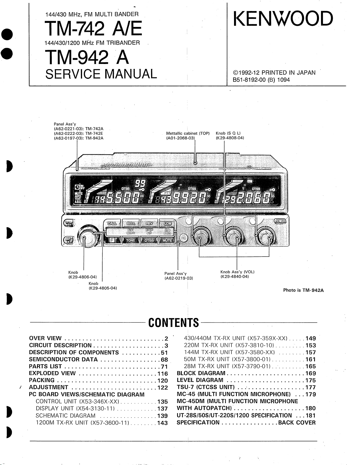
Kenwood TM-742 User manual
Other Kenwood Car Video System manuals

Kenwood
Kenwood DNX7120 - Navigation System With DVD player User manual

Kenwood
Kenwood KVT-M707 User manual

Kenwood
Kenwood LZ-702IR - LCD Monitor User manual

Kenwood
Kenwood DDX719WBTL User manual

Kenwood
Kenwood DDX6036 User manual

Kenwood
Kenwood DDX9907XR User manual

Kenwood
Kenwood KVT-50DVDRY User manual

Kenwood
Kenwood DNX5120 - Navigation System With DVD player User manual

Kenwood
Kenwood LZH-100W - DVD Player With LCD Monitor User manual

Kenwood
Kenwood DDX5034M User manual

Kenwood
Kenwood KOS-L702 User manual

Kenwood
Kenwood VZ-7000N User manual

Kenwood
Kenwood KVT-617DVD User manual

Kenwood
Kenwood DDX7032 User manual

Kenwood
Kenwood KVT-729DVD User manual

Kenwood
Kenwood KVT-526DVD User manual

Kenwood
Kenwood DNX7120 - Navigation System With DVD player User manual

Kenwood
Kenwood KVT-526DVD User manual

Kenwood
Kenwood VZ907 User manual

Kenwood
Kenwood DMX125DAB User manual