Kenwood RD-M23 User manual

70%
COMPACT AUDIO SYSTEM
RD-M23
SERVICE MANUAL
(For M,X type) © 2001-9 PRINTED IN KOREA
B51-5756-00 (K/K) 547
Front cabinet
(A60-2147-08)
Knob
(K29-8085-08)
Clear panel(DISK)
(B10-3764-08)
In compliance with Federal Regulations, following are repro-
duction of labels on, or inside the product relating to laser prod-
uct safety.
KENWOOD-Corp. certifies this equipment conforms to DHHS
Regulations No.21 CFR 1040. 10, Chapter 1, subchapter J.
DANGER : Laser radiation when open and interlock defeated.
AVOID DIRECT EXPOSURE TO BEAM.
Plate
(B03-3900-08)
CD lid
(J19-6268-08)
Knob
(K29-8084-08)
Rear panel
(A80-4203-08)
Digital out jack
(W02-2878-08)
Bottom cabinet
(A10-3564-08)
Socket
(E03-0384-08)
Terminal
(E21-0040-08)
Terminal
(E70-0149-08)
Headphone jack
(E11-0944-08)
Socket
(E63-1228-08)

AC power lead x1
(E30-7240-08): X
(E30-7237-08): M
Remote control x1
(A70-1547-08)
Battery cover(A09-1243-08)
FM antenna x1
(T90-0891-08)
AM loop antenna x1
(T90-0890-08)
"AAA" size battery
(UM-4, R03, HP-16 or similar)x2
RD-M23
2
CONTENTS / ACCESSORIES
CONTENTS / ACCESSORIES .................................. 2
DISASSEMBLY FOR REPAIR....................................3
BLOCK DIAGRAM ......................................................5
TROUBLE SHOOTING ...............................................7
TEST MODE .............................................................10
ADJUSTMENT ..........................................................13
WAVR FORM............................................................15
PARTS DESCRIPTIONS ..........................................16
PC BOARD .............................................................. 17
SCHEMATIC DIAGRAM .......................................... 21
EXPLODED VIEW ....................................................29
PARTS LIST..............................................................31
SPECIFICATIONS ......................................Back cover
Contents
Accessories
Troubleshooting
If trouble occurs
When this product is subjected to strong external interference
(mechanical shock, excessive static electricity, abnormal supply
voltage due to lightning, etc.) or if it is operated incorrectly, it may
malfunction.
If such a problem occurs, do the following:
Caution:
This operation will erase all data stored in memory including clock,
timer settings, tuner preset, and CD programme.
1 Set the unit to the stand-by mode and turn the power on
again.
2 If the unit is not restored in step 1, unplug and plug in the
unit, and then turn the power on.
3 If neither step 1 nor 2 restores the unit, do the following:
Press the ON/STAND-BY button to enter the power stand-by
mode.
Unplug the AC power lead from the AC INPUT socket on the
unit.
Whilst pressing down the MEMORY/SET button and the /
button, plug the AC power lead into the AC INPUT socket on
the unit.
AC INPUT
Attention
Please contact our KENWOOD Service Department in your side if you want the service information; Circuit Description. Full
Described Parts list and so. Information is available to you by internet from us.
CLASS 1
LASERPRODUCT
The markingthisproducthas been
classifiedasClass1.Itmeansthatthere
isno dangerof hazardousradiatio
outside theproduct.

RD-M23
3
DISASSEMBLY FOR REPAIR
1
Rear panel/Terminal PWB
1. Screw .................. (A1) x7 8-1
2. Socket ................. (A2) x2
3. Screw .................. (A3) x3 8-1,2
2 Top cabinet 1. Screw .................. (B1) x2 8-2
2. Hook .................... (B2) x5
3. Flat Cable ............ (B3) x1
4. Socket ................. (B4) x7
3 Tuner PWB 1. Screw .................. (C1) x2 9-1
2. Socket ................. (C2) x1
4 Power PWB 1. Socket ................. (D1) x1 9-1
2. Hook .................... (D2) x1
5 Main PWB 1. Socket ................. (E1) x1 9-1
2. Screw .................. (E2) x8
6 Display PWB 1. Screw .................. (F1) x4 9-2
2. Hook .................... (F2) x4
7 CD Mechanism 1. Screw .................. (G1) x4 9-2
8 Gear Box 1. Screw .................. (H1) x1 9-2
2. Holder .................. (H2) x1
3. Lever ................... (H3) x1
4. Screw .................. (H4) x2
5. Lever ................... (H5) x1
9 LED PWB 1. Screw .................. (J1) x1 9-2
STEP REMOVAL PROCEDURE FIGURE
Note:
After removing the connector for the optical pickup from the
connector, wrap the conductive aluminium foil around the
front end of connector remove to protect the optical pickup
from electrostatic damage.
Caution on Disassembly
Follow the below-mentioned notes when disassembling
the unit and reassembling it, to keep it safe and ensure
excellent performance:
1. Take compact disc out of the unit.
2. Be sure to remove the power supply plug from the wall
outlet before starting to disassemble the unit.
3. Take off nylon bands or wire holders where they need to
be removed when disassembling the unit. After servicing
the unit, be sure to rearrange the leads where they were
before disassembling.
4. Take sufficient care on static electricity of integrated
circuits and other circuits when servicing.
(A1) x2
ø3 x10mm
(A1) x3
ø3 x10mm
(A1) x2
ø3 x10mm
Rear Panel
Top Cabinet
(A2) x2
(A3) x2
ø3 x10mm
Rear Panel
Terminal PWB
Figure 8-1
(B1) x2
ø2.5 x8mm
(B4) x2
(A3) x1
ø3 x8mm
Lug
(B4) x4 (B3) x1
Hook
(B2) x3
HOOK
(B2) x2
(B4) x1
CD Mechanism
Main PWB
Power PWB
Hook
Up
Slide
Bottom Cabinet
Top Cabinet
Top Cabinet
Bottom Cabinet
Figure 8-2
(C1) x1
ø3 x8mm
(E2) x7
ø3 x8mm
(E2) x1
ø3 x14mm
(D2) x1
(C1) x1
ø3 x6mm
(D1) x1
(E1) x1
Power PWB
Holder PWB
Tuner PWB
Main PWB
(C2) x1
Tuner PWB
(C2) x1
Main PWB
Hook
Bottom Cabinet
Figure 9-1
Figure 9-2
(G1) x4
ø2.5 x10mm
(H1) x1
ø3 x8mm
(H2) x1
(H5) x1
(H4) x2
ø2.5 x10mm
(J1) x1
ø2.5 x10mm
(F1) x4
ø2.5 x10mm
Hook
(F2) x4
Display PWB
LED PWB
Switch
PWB
Gear Box
CD Mechanism
Top Cabinet
Holder PWB
(H3) x1
Bracket

RD-M23
4
DISASSEMBLY FOR REPAIR
How to remove the CD lid (See Fig. 10-1.)
Perform steps 1,2 and 8 of the disassembly method to remove
the gear box.(See page 8,9)
1. Remove the switch PWB.
2. Remove the screws (A1) x 4 pcs., to remove the gear box
lid.
3. Remove the gears (A2) x 1 pc. and (A3) x 1 pc.
4. Remove the screws (A4) x 2 pcs., to remove the motor.
Caution:
Be careful so that the gear is not damaged.
(The damage gear emits noise during searching.)
Figure 10-1
Figure 10-2
(A1) x1
ø2.5 x10mm
(A1) x3
ø2.5 x12mm
(A2) x1
(A3) x1
(A4) x2
ø2 x5mm Switch PWB
CD Lid Motor
CD MECHANISM SECTION (See Fig. 10-2.)
Perform steps 1,2 and 7 of the disassembly method to remove
the CD mechanism.(See page 8,9)
1. Remove the mechanism cover, paying attention to the
pawls (A1)x 4 pcs.
2. Remove the screws (A2) x 2 pcs., to remove the shaft (A3)
x 1 pc.
3. Remove the stop washer (A4) x 1 pc., to remove the gear
(A5) x 1 pc.
4. Remove the pickup.
Note:
After removing the connector for the optical pickup from the
connector, wrap the conductive aluminium foil around the
front end of connector remove to pretect the optical pickup
from electrostatic damage.
Pickup unit
(A2) x2
ø2.6 x6mm
(A1) x4
CD Mechanism
Shaft
(A3) x1
Gear
(A5) x1
Stop Washer
(A4) x1
Mechanism Cover
REMOVING AND REINSTALLING THE MAIN PARTS

RD-M23
5
BLOCK DIAGRAM
2
1
VOLTAGE
REGULATOR
3
1
3
4
2
1
USWD_5R6V
P_CONT
D_GND
3
2
1
AC INPUT
SOCKET
AC 110/127/220/
230~240V, 50/60Hz
AC POWER SUPPLY CORD
VOLTAGE
SELECTOR
POWER
TRANSFORMER
(SUB)
FROM
DISPLAY PWB
POWER PWB-B
CNP651
SO655
SW651
IC681
KIA7805API
D688
1N4004
RLY601
CNP707
T681
D681~D684
Q683
Q681
4
3
2
1
4
3
2
1
3
5
5
7
7
9
9
1
POWER
TRANSFORMER
(MAIN)
TF
T651
T2.5A L 250V
CNP801
F651
T1.25A L 250V
F653
Q606
Q607
D651~D654
D657~D660
Q801
Q101
Q102
Q601
Q602
Q605
Q603
Q604
Q608
Q609
CD +B
CNP652
FROM
DISPLAY PWB
+B
CD_6R2V
+B2
+B3
+B4
+B6
M_12V
A_12V
POWER AMP.
IC901
LA4282 L-CH
L-CH
R-CH
R-CH
L-CH R-CH
SPEAKER TERMINAL
+
+
SO601
HEADPHONES
1
2
3
4
5
9
10
J601
VSS
VDD
IC401
LC75342M
15 14 13 12 11 10 9
17 18 19 20 21 22 23 24 25 26 27 28 29
16
8 7 6 5 4 3 2 1
CE
DI
30
CL
LOGIC
TUN L
CD L
TUN R
R-CH OUT
L-CH OUT
A_12V
NC
FUNCTION/VOLUME
EQUALIZER
Q901 Q902
Q908 Q907
Q861
Q802
AUX R
AUX L
CD R
7654321 8910 11 12 13 14 15
CNP702
CLID_SW
CLID_UP
CLID_PRO
CLID_DW
BUCK
BUS2
BUS0
BUS1
BUS3
CCE
CD_RES
PU_IN
LIGHT
CD_STB
DIMMER
SBAD
FEO
FEN
VRO
RFRP
RFIS
RFGO
RFGC
AGCI
RFO
GND
RFN
TEO
TEN
2VRO
TEB
SEL
LDO
MDI
TN1
TPI
FPI
FNI
VCC
SERVO PRE AMP.
IC801
TA2109F
SERVO/SIGNAL CONTROL
IC802
TC9462F
DOUT
TERMINAL
PWB
VSS
VSS
VSS
AVSS
XVSS
TESIOO
TESIN
TESI01
VSS
VSS
PXI
DVSL
DVSR
PDO
TMAX
VCOREV
RFI
RFCT
LPFN
LPFO
PVREV
TSIN
VREF
X801
16.93MHz
XO
XI
VDD
VDD
VDD
VDD
VDD
XVDD
AVDD
2VREF
SEL
RFGC
TEBC
FOO
TRO
TEI
TEZI
RFRP
FEI
SBAD
P2VREF
SWITCHING
MUTE
VOLTAGE
REGURATOR
VOLTAGE
REGURATOR
+B6
R-CH
L-CH
SO401
VIDEO/AUX
INPUT
CD LID
MOTOR DRIVER
1
23
5
67
8
9
IC805
TA7291S
11 10 9 8 7 6 5 4 3 2 1
CE
CL
DI
SD
FM ST
DO
A_12V
D_GND
TUN L
TUN R
A_GND
11
1 2 3 4 5 6 7 8 9 10
SD
STEREO
DO
CE
DI
CL
CD +B
P_MUTE
P_STB
D_GND
A_12V
+B1
+B3
+B6
+B2
+B4
CNP703
CNP307
TO
TUNER PWB
FROM
DISPLAY PWB
FROM
DISPLAY PWB
LED PWB
SWITCH PWB
CD LID
OPEN/CLOSE
SW802
CD LID
OPEN/CLOSE
MOTOR
M
M801
FOCUS/TRACKING/
SPIN/SLED DRIVER
1234
5
6
7
8
9
9
10111213
16 17 18 19 21 22 23 24 25 26 27 28
PO1-
PO1+
VO3-
VO3+
VIN3
VG3
VCC
VCC
BIAS
VG4
VIN4
VO4+
VO4-
OPO
VO2-
VO2+
VIN2
VG2
GND
GND
GND
MUTE
REG O
TRB
VG1
VIN1
VO1+
VO1-
IC804
MM1469XH
SPINDLE
MOTOR
SLED
MOTOR
PICKUP IN
SP+
SP–
SP+
SL–
PU-IN
GND
FO
TR
+
–
–
+ M
M
CD MOTOR PWB
NM802
NM801
NSW801
CD_7V
5V +B2
+B4
+B7
+B7
+B7
A
C
B
F
E
+B7
+B7
+B7
LD
MON
FOCUS COIL
1/2V
5V
TRACKING COIL
PICKUP UNIT
23
24
22
21
20
19
18
17
16
45
40
38
34
33
32
31
30
28
50
56
57
51
52
48
49
46
47
43
42
44
15
14
13 12
11
10
9
8
7
6
5
4
3
2
1
DIGITAL
OUT 3
2
1
J801
5355
FMO
DMO
100
90
97
96
93
92
91
78
79
BUS0
BUS1
BUS2
BUS3
BUCK
/CCE
/RST
85
82
RO
LO
14
23
39
62
76
80
94
6152436 63 71 72 73 74 77 95 81 86
D_GND
A_GNDD_GND
D_GND
M_GND
M_GND
M_GND
M_GND
25
MAIN PWB
AC 110/127/220/
230~240V, 50/60Hz
5 12910 113 742
IN2
POWER
–GND1
VCC
OUT1
FIL
OUT2
GND
NF1
110V
127V
220V
230~240V
F654
2A 250V
TF

AM
GND
FM
75ohms
SO301
VSM
AM RF
OUT
OUT
OUT
OUT
IN
IN
CUT
AM LOW
FM/AM
MPX VCO
MPX IN
MO/ST
L-CH
R-CH
FM AFC
AM OSC
AM OSC
(AM/FM)
PHASE
PHASE
IF OUT
VCC
FM DET
STEREO
SD
GND
AM IF
REG
AM MIX
OUT
IN
IN
FM IF
23 22 21 20 19 18 17 16 15 1424 13
121110987654321
PLL(TUNER)
111098765431
PD
IF IN
AM IN
FM IN
VDD
AIN
AOUT
VSS
X OUT
22 21 20 19 18 17 16 15 14 13 12
FM
FM
MUTE
CE
DI
CL
DO
MO/ST
IF REQ
X IN
IC302
LC72131
FM FRONT END
123456 7 9
8
IC301
BF301
BAND PASS
FILTER
TA7358AP
123
TP301
456kHz
X351
32.768kHz
8MHz
Q351
Q360
ZD351 10
11
1
2
3
4
5
8
9
6
7
SD
FM ST
DO
CL
CE
DI
A_12V
D_GND
TUN_L
TUN_R
A_GND
TO
MAIN PWB
CNS307
TUNER PWB
38541
1
100
67
57
56
20
59
66
65
64
63
62
61
60
58
53
54
51
39 46 49 5032
47
8
4
LCD701
LCD DISPLAY
1
2
3
4
5
6
7
8
9
10
11
12
13
14
15
LIGHT
BUS0
BUS1
BUS2
BUS3
BUCK
CCE
CD_STB
CLID_DW
CLID_UP
CLID_PRO
CLID_SW
CD_RES
PU-IN
DIMMER
LIGHT
BUS0
BUS1
BUS2
BUS3
BUCK
CCE
CD_STB
CLID_DW
CLID_UP
CLID_PRO
CD_RES
PU-IN
DIMMER
B-LIGHT
1
2
3
4
5
6
7
8
9
10
11
12
13
14
15
TO
MAIN PWB
TO
MAIN PWB
TO
POWER PWB
TO
MAIN PWB
CNS702
CNW702
REMOTE
SENSOR
RX701
3
2
1
3
4
2
1
2
1
CNW707
CNS707CNS652
RESET
VLC1
VLC2
VLC3
7
6
5
MMOD
VREF–
VREF+
VSS
15
24
14
11
SYS_STOP
POWER
3837
13
12
10
9
X701
X702
OSC1
OSC2
XO
XI
CLID_SW
SW711~713
SW721,722
SW725~727
SW709
SW718
SW710 KEY1
KEY2
18
17
16
SYSTEM MICROCOMPUTER/
FL DRIVER
IC701
IX0039SJ
D_GND
A_24VA_12V
P_STB
P_MUTE
CD+B
DI
CE
CL
DO
STEREO
SD
11
10
9
8
7
6
5
4
3
2
1
11
10
9
8
7
6
5
4
3
2
1
CNW703
CNS703
CD+B
STEREO
SD
DI
CL
DO
CE
28272625
SURR
P–STB
P–MUTE
454443
DISPLAY PWB
Q708
Q707
Q709
Q706
ANTENNA
TERMINAL
AM Band
Coverage fL
FM MUTE
LEVEL
AM IF
FM IF
AM
Tracking fL
FM RF
VD301
VD303
VD302
FM IF DET/
FM MPX/AM IF
IC303
LA1832S
+5V
+5V
VT
+5V
+5V
+B
FM +B
+5V
FM +B
+5V
T302
T306
T304
T351
CF303
L302
FM ANT.
FM Band
Coverage fL
FM +B
FM +B
L303
FM OSC.
CF302
FM IF FM IF
CF352
CF351
AM IF
SWITCHING
SWITCHING
RESET
SWITCHING
Q306
Q302
Q701 Q702
Q703
VR351
X352
4.5MHz
VOLTAGE
REGURATOR
COM0
COM3
SEG0
SEG33
REMOCON
P_CONT
USWD_5R6V
D_GND
P–CONT
VDD
GND
LED701 LED702
LED PWB
RD-M23
6
BLOCK DIAGRAM

RD-M23
7
Cleaner Liquid Cleaning Disc
PARTS CODE: UDSKA0004AFZZ
HOW TO USE
1. Using the brush in the cleaner cap, apply 1 or 2 drops of the cleaning fluid to the brush on the CD cleaner disc which has
the mark next to it.
2. Place the CD cleaner disc onto the CD disc tray with the brush side down, then press the play button.
3. You will hear music for about 20 seconds and the CD player will automatically stop. If it continues to turn, press the stop button.
CAUTION
The CD lens cleaner should be effective for 30 - 50 operations, however if the brushes become worn out earlier then please
replace the cleaner disc.
If the CD cleaner brushes become very wet then wipe off any excess fluid with a soft cloth.
Do not drink the cleaner fluid or allow it to come in contact with the eyes. In the event of this happening then drink and / or
rinse with clean water and seek medical advice.
The CD cleaner disc must not be used on car CD player or on computer CD ROM drives.
All rights reserved. Unauthorized duplicating, broadcasting and renting product is prohibited by law.
When the CD does not function
When the CD section does not operate when the objective lens of the optical pickup is dirty, this section may not operate. Clean
the objective lens, and check the playback operation. When this section does not operate even after the above step is taken,check
the following items.
Remove the cabinet and follow the troubleshooting instructions.
"Track skipping and/or no TOC (Table Of Contents) may be caused by build up of dust other foreign matter on the laser pickup
lens. Before attempting any adjustment make certain that the lens is clean. If not, clean it as mentioned below."
Turn off the power, and wipe the lens softly using a cleaning paper moistened with commercially available cleaning solution so
as not to damage it.
Be careful not to touch the lens with bare hands.
Dust gradually accumulates on the objective lens during use, and it may degrade performance.
To avoid this problem, use a cleaning disc designed for CD optical pickup lenses.
Make sure that the disc is normal, and set the CD TEST MODE (STEP 1).
Is the measured voltage as specified in circuit diagram? Check the main unit power supply circuit.
No
Yes
No
Is "Er-CD01" displayed"?
Yes
Move the pickup to most internal circumference side of disc.
Turn the power off and reset the CD TEST MODE (STEP 1).
Is "PU ERROR " not displayed?
Yes
Check the PWB pattern between pin 59 (CD_RES) of IC701 and
pin 100 (/RST) of IC802.
No
Is +5V applied to pin 100 (/RST) of IC802?
Yes
Is CD Lid switch SW802
ON condition ?
No
Does the CD TEST MODE advance from "STEP 2"?
Yes
Check the between pattern IC701 and SW802 If OK.
Check the main unit power supply circuit.
No
Does the laser come on in CD TEST MODE "STEP 2"? Check the procedure in "LASER FAILURE".
Yes
Does the CD TEST MODE advance from "STEP 3" to "STEP
4"?
Check the procedure in "FOCUS FAILURE".
Yes
Yes
Does the spindle motor rotate normally when the CD TEST
MODE changes from "STEP 4" to "STEP 3"?
Yes
Is the HF output on pin 38 of IC802 in CD TEST MODE "STEP 5"? Check the procedure "HF ERROR".
Yes
No
No
No
No
Check the pattern between pin 58 (PU_IN) of IC701 and
CNW803/CNS803.
Check the between CNW803/CNS803 and PU-IN switch.
Set ON condition the CD
Lid switch.
Check the procedure in "SPINDLE MOTOR CLV SERVO
FAILURE".
No
Does the sled motor
move ?
No
Does the sound heard when the optical pickup move to the
selected play by the FF /REW key.
Check the procedure "NO SOUND"
No
Yes
Check the procedure in
"SLED MOTOR
OPERATING FAILURE ".
Does the LCD track number and time indicator work properly ? Check the pattern between IC701 and LCD701.
Yes
No
Is "Er-CD01 "
displayed ?
No
Turn the power off and then back on.
Does the unit initialize properly and start playback when PLAY
key is pressed?
Check the pattern between pin 58 (PU_IN) of IC701
and CNW803/CNS803. Check the between CNW803/
CNS803 and PU-IN switch.
No
Yes
Check the procedure in
"HF ERROR".
Yes
Does the unit play in order in the FF mode? Check the procedure in "TRACK SEARCH FAILUR".
Yes
Does playback continue for 30 seconds after the start of
playback ?
Check the procedure in "SLED SERVO FAILURE".
Yes
Normal
No
No
Yes
TROUBLE SHOOTING

RD-M23
8
Check the PWB pattern between emiter of Q607 and emiter of
Q861.
• Laser failure.
Is 0V applied to the pin 57 (SEL) of IC802 ?
Yes
No
Does the laser come on when pattern cut between pin 8 (SEL) of
IC801 and pin 57 (SEL) of IC802 ?
Check the PWB pattern between IC701 and IC802 (BUCK/CCE/
BUS0~3)
Yes
Yes
No
Check the peripheral parts of IC801 and Q801. If it is normal, the
optical pickup is faulty.
No
Check CNP802/CNW3. If it is normal, the optical pickup is
faulty.
Is approx. 2V applied to the collector of Q801.
• Focus failure.
Does the optical pickup move up and down when the disc is
removed?
Is the following waveform ouput at the pin 43 (FEI) of IC802
when the disc is set?
Is the waveform shown above input at the pin 44 (SBAD) of
IC802?
Yes
Yes
No
No
The optical pickup is faulty.
Check as stated in item "FOCUS SERVO SAWTOOTH WAVE
FAILURE".
Yes
Check the periphery of IC801 and CNP802/CNW3. Is it normal?
No
Check the pattern between pin 13 of IC801 and pin 44 of IC802.
Check the periphery of IC801 and CNP802/CNW3.
IC801 is faulty.
Yes
Is +6.2V applied to the emiter of Q861 ?
Is +5V applied to the collector of Q861 ?
Yes
No
No
Check the peripheral parts of IC804 and Q861.
Is +5V applied to the pin 62 (VDD) of IC802 ?
Is +5V applied to the pin 1 (VCC) of IC801 ?
Yes
No
No
Check the PWB pattern between collector of Q861 and pin 62 of
IC802.
Check the PWB pattern between collector of Q861 and pin 1 of
IC801.
pin 43
(FEI)
pin 48
(FOO)
pin 44
(SBAD)
Yes
Yes
•Focus servo sawtooth wave failure.
Is +6.2V applied to the pins 21 and 22 (VCC) of IC804 ?
Is sawtooh wave output to the pin 48 (FOO) of IC802 ? IC802 is faulty.
No
Yes
Yes
Is sawtooth wave obtained between pins 26 and 27 of IC804 ?
No No
Check the PWB pattern
between pin 7 of IC804
and pin 60 (CD STB) of
IC701.
Is +5V applied to the pin 7
(MUTE) of IC804 ?
Check the PWB pattern between pin 48 (FOO) of IC802 and pins
24 and 25 of IC804. If OK. IC804 is faulty.
Check the PWB pattern between pin emiter of Q607 and IC804.
No
Is sawtooth wave obtained between pins 13 and 16 of
CNP802/CNW3 ? (as shown above)
Yes
Check the PWB pattern between CNP802/CNW3 and IC804.
No
CNP802/CNW3 connection failure or optical pickup failure.
Yes
•Spindle motor clv servo failure.
Is above wave obtained between pins 11 and 12 of IC804 ?
Is following wave output to the pin 55 (DMO) of IC802 when
the CD TEST MODE "STEP 3" is changed to " STEP 4" ? No
Yes
Check the procedure in "HF ERROR".
If OK. IC802 is faulty.
Check the PWB pattern between pin 55 (DMO) of IC802 and pins
9 and 10 of IC804. If OK. IC804 is faulty.
No
Is above wave obtained between pins 9 and 12 of CNP802/
CNW3 ?
Yes
Check the PWB pattern between CNP802/CNW3 and IC804.
No
CNP802/CNW3 connection failure or optical pickup failure.
Yes
DMO
Yes
1.5~2.5sec
1.5~2.5sec
TROUBLE SHOOTING

RD-M23
9
•HF error.
Yes
Yes
Is output (tracking error signal) obtained at the pins 46 (TEI)
and 47 (TEZI) of IC802 the CD TEST MODE "STEP 4" is
changed to "STEP 5"?
Is output (HF signal) obtained at the pin 38 (RFI) of IC802
when the CD TEST MODE "STEP 4" is changed to "STEP 5"?
Is output (HF signal) obtained at the pins 41 (RFZI) and 42
(RFRP) of IC802 when the CD TEST MODE "STEP 4" is
changed to "STEP 5"?
No
No
•No sound.
No sound from both L and R-ch?
Yes
Is +4.5V applied to pin 83 (DVDD) of IC802?
No
Check the PWB pattern between pin 49 (TRO) of IC802 and pin 19
of IC804.
Check the periphery of IC804 and CNP802/CNW3.
If OK. Optical pickup failure.
Check the periphery of IC801.
Check the PWB pattern between pin17 (RFRP) of IC801 and pins
41 (RFZI) and 42 (RFRP) of IC802.
If OK. IC801 is faulty.
No
Yes
Normal.
Check the interval between the pins 82 or 85 of IC802 and the pins
2 or 5 of IC901.
No
Check the PWB pattern between R819 and Q861.
Yes
Is signal of pins 82 and 85 of IC802 output?
No
Check the peripheral parts of IC802. If OK, IC802 is faulty.
Yes
The main PWB is faulty.
Check the periphery of IC801.
Check the PWB pattern between
pin 12 (TEO) of IC801 and pins 46
and 47 of IC802.
Is it normal ?
Is output obtained at the pins 3 and
8 of CNP802/CNW3.
Optical pickup failure.
IC801 is faulty.
Check the periphery of IC801.
Check the PWB pattern between pin 19 (RFGO) of IC801 and pins
38 (RFI) of IC802.
If OK. IC801 is faulty
Is output obtained at the pins 4 and
5,6 of CNP802/CNW3. Optical pickup failure.
Is the following wave output to the pin 55 (DMO) of IC802
when the CD TEST MODE "STEP 4" or "STEP 5"?
Check the periphery pins 28~32 of IC802.
If OK. IC802 failure.
No
No
No
Yes
Yes
No
Yes
Yes
test mode "step 4" test mode "step 5"
TEI
TEZI
test mode "step 4" test mode "step 5"
RFI
test mode "step 4" test mode "step 5"
RFZI
RFRP
test mode "step 4" test mode "step 5"
DMO
•Sled motor operation failure.
Yes
Yes
Is following sled feed signal output the pin 53 (FMO) of IC802
when FF /REW key is pressed after the CD TEST
MODE "STEP 1" is seted?
Is sled feed signal output the pins 1 and 2 of IC804?
Is sled feed voltage applied between both terminals of sled
motor?
No
Check the peripheral parts of IC804. If OK, IC804 is faulty.
No
C801 is faulty.
Check the CNW803/CNS803.
No
Yes
Check the CD mechanism (periphery of sled motor).
If the sled motor does not run when DC2.0V is applied to
both terminals of sled motor, the sled motor is faulty.
•Sled servo failure.
Yes
Is following sled signal output the pin 53 (FMO) of IC802
during playback?
Normal.
No
IC802 is faulty.
•Track search failure
Does the sled motor run in FF/REW state when the SERVO
TEST MODE "STEP1" is set?
Is the following wave output to the pin 49 (TRO) of IC802
during track search in normal playback?
Is the following wave output to the pins 12 (TEO) of IC801
during track search in normal playback?
Yes
Yes
No Check as stated in item "SLED MOTOR OPERATION FAILURE".
No IC802 failure.
No Check the PWB pattern between pin 49 (TRO) of IC802 and pin
19 of IC804.
Check the PWB pattern between pins 17 and 18 of IC804 and
Optical pickup.
If OK. Optical pickup failure.
Yes
Is the above wave output to the pins 46 (TEI) and 47 (TEZI) of
IC802 during track serch in normal playback? No Check the PWB pattern between pin 12 (TEO) of IC801 and pins 46
and 47 of IC802. If OK. IC801 failure.
Normal.
Yes
Yes
Is following sled feed signal output the pins 3 and 4 of IC804
when FF /REW key is pressed after the CD TEST
MODE "STEP 1" is seted?
Check the PWB pattern between pin 53 of IC802 and pins 3 and 4
of IC804.
No
Is the following wave output to the pin 41 (RFZI) and 42
(RFRP) of IC802 during track search in normal playback? No Check the PWB pattern between pin 17 (RFO) and 18 (RFIS), 19
(RFRP) of IC801 and pins 41 and 42 of IC802. If OK. IC801 failure.
Yes
TRO
TEO
TEI
TEZI
FF REW
FMO
FMO
RFZI
RFRP
FF REW
SL ±
TROUBLE SHOOTING

RD-M23
10
TEST MODE
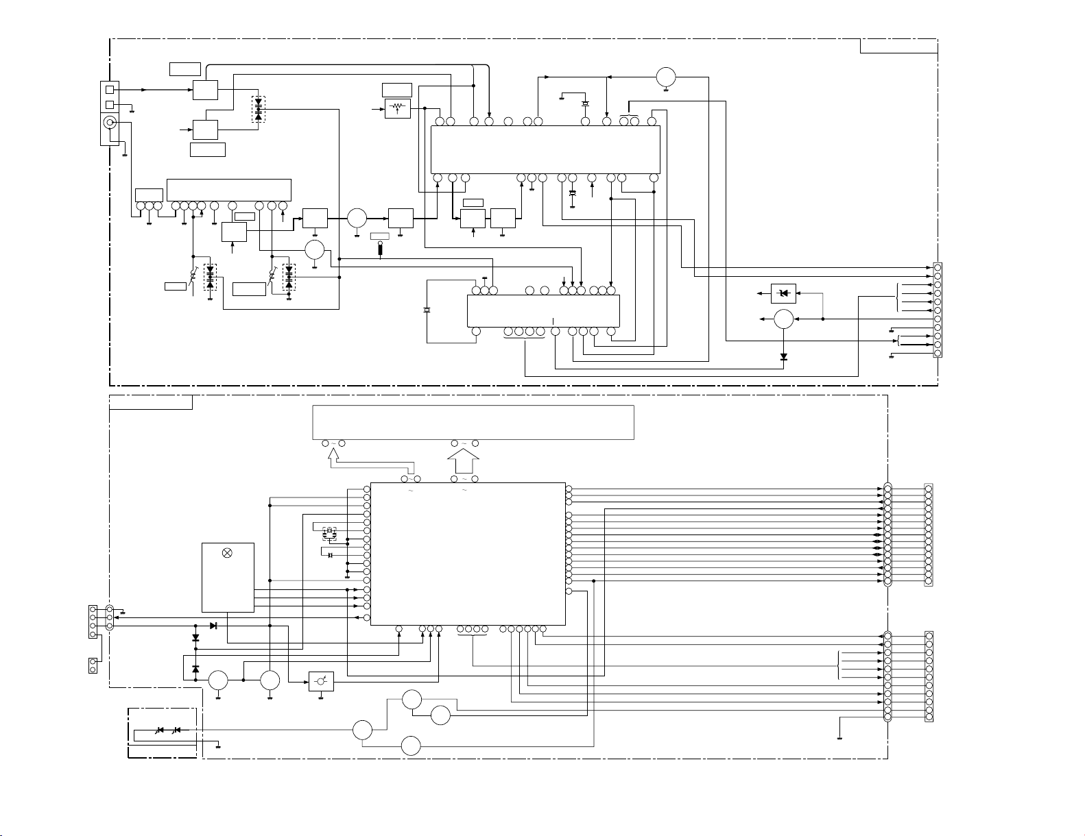
2. CD Test Mode (TEST 1)
In the CD test mode the operation of each step is possible even if the LID-SW is off. If focus cannot be taken in step 3 or any error
is processed, it is impossible to proceed to the next step. During error processing, end the test mode by pressing the ON/STAND-
BY button or return to the step 1 by pressing the CD STOP button. Any other operations are inhibited.
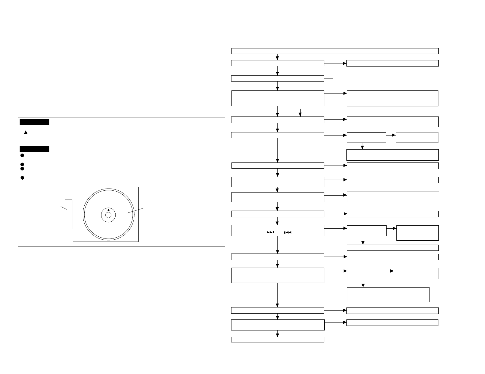
1. Step 1 Mode
When the CD test mode is obtained, the following display lights up. Then CD initialization operation flow proceeds up to CD
STB off to wait for the following buttons to be pressed.
One second after display lights up
Press the following buttons in this state to obtain the operations specified below.
"POWER" ................. Test mode and power turned off to shift to the ordinary standby mode.
"FF/FWD" ................. After the pickup returns to the innermost periphery, it slides toward the outer periphery while this button
is pressed.
"REW/REV" ..............After the pickup returns to the innermost periphery, it slides toward the inner periphery while this button
is pressed. If PICKUP IN is on, input is invalid.
"PLAY" ..................... Shift to step 2
"STOP" ..................... Invalid
"FUNCTION" ............ Shift to step 5
* In case of initialization, the pickup is moved toward the inner periphery. Any buttons other than "ON/STAND-BY" button are
not accepted until the shift of pickup to the inner periphery is completed at this time. If PICKUP IN SW ON cannot be detected
within 10 seconds, the slide motor stops, and the following error display appears. Press the ON/STAND-BY button to end
the test mode, or press the CD STOP button to return to step 1. Any other operations are inhibited.
The test mode applied to this microcomputer has three modes, namely the ordinary test mode for adjustment or measurement,
the aging test mode, and the self-diagnosis test mode for self-judgment in case of final product inspection.
1. Turning on the test mode
For obtaining each test mode, press the ON/STAND-BY button, while keeping pressing the following two buttons in the ordinary
stand-by mode (power off ). In this case, the main unit buttons are valid. When turning the ON/STAND-BY on with remote control
buttons, test modes are not obtained.
[Ordinary test mode]
1. CD Test Mode (TEST 1).....................................REW/PRESET DOWN + VOLUME UP
2. Tuner Test Mode (TEST 2).................................REW/PRESET DOWN + CD PLAY
3. Electronic Volume Test Mode (TEST 3)............. REW/PRESET DOWN + FF/PRESET UP
4. Timer Test Mode (TEST 4).................................FUNCTION + VOLUME UP
5. LCD Test Mode (TEST 5)...................................FUNCTION + FF/PRESET UP
6. Electric CD Lid Aging Test Mode (TEST 8)........ FUNCTION + CD PLAY
FUNCTION + VOLUME DOWN
[Self-diagnosis Test Mode]
1. Button input diagnosis test mode (TEST6).…....
Processes are different depending on destinations at initial settings.
The time display always indicates "0:00".
Press the following buttons in this state to obtain the operations specified below.
"POWER" ................ Test mode and power turned off to shift to the ordinary standby mode.
"FF/FWD" ................ The pickup slides toward the outer periphery while this button is pressed.
"REW/REV" ............. The pickup slides toward the inner periphery while this button is pressed. If PICKUP IN is on, input is
invalid.
"PLAY" ..................... Shift to step 5
"STOP" .................... Return to step 1
"FUNCTION" ........... Shift to step 5
*If the focus is not received, the process returns to step 1.
4. Step 4 Mode
The CLV servo ON command (8600) is transmitted to wait for the following buttons to be pressed. (The disc is rotated for CLV
lock.)
Press the following buttons in this state to obtain the operations specified below.
"POWER" ................ Test mode and power turned off to shift to the ordinary standby mode.
"FF/FWD" ................ The pickup slides toward the outer periphery while this button is pressed.
"REW/REV" ............. The pickup slides toward the inner periphery while this button is pressed. If PICKUP IN is on, input is
invalid.
"PLAY" ..................... If focus has been taken, shift to step 4 is executed. If not, acceptance is inhibited.
"STOP" .................... Return to step 1
"FUNCTION" ........... Shift to step 5
*If the focus is not received after it has been taken, the process returns to step 1.
3. Step 3 Mode
While the laser keeps lighting, CD initialization operation flow proceeds up to 'CLV servo ON' to wait for the following buttons
to be pressed.(Focus servo turned on for focus search)
The focus search is repeated to take focus.
Press the following buttons in this state to obtain the operations specified below.
"POWER" ................ Test mode and power turned off to shift to the ordinary standby mode.
"FF/FWD" ................ The pickup slides toward the outer periphery while this button is pressed.
"REW/REV" ............. The pickup slides toward the inner periphery while this button is pressed. If PICKUP IN is on, input is
invalid.
"PLAY" ..................... Shift to step 3
"STOP" .................... Return to step 1
"FUNCTION" ........... Shift to step 5
2. Step 2 Mode
Press the "CD PLAY" button in this mode to transmit the laser lighting command LDON (8400) and turn on the laser. Any other
operations are not performed in this case.

RD-M23
11
Press the following buttons in this state to obtain the operations specified below.
"POWER" ................. Test mode and power turned off to shift to the ordinary standby mode.
"FF/FWD" ................. The pickup slides toward the outer periphery while this button is pressed.
"REW/REV"..............The pickup slides toward the inner periphery while this button is pressed. If PICKUP IN is on, input is
invalid.
"PLAY" ..................... Invalid
"STOP" ..................... Return to step 1
"FUNCTION" ........... Shift to step 6
"MEMORY" .............. Shift to step 7
*If the is not received, the process returns to step 1.
Other cautions
•TOC IL is not available for this test mode.
5. Step 5 Mode
When the CD initialization operation flow is completed, the mute is turned off, and playback is started. Even if playback
reaches the outermost periphery of disc, the operation does not stop. The LCD display indicates the playback passage time
as in case of ordinary CD playback.
Press the following buttons in this state to obtain the operations specified below.
"POWER" ................. Test mode and power turned off to shift to the ordinary standby mode.
"FF/FWD" ................. The pickup slides toward the outer periphery while this button is pressed.
"REW/REV"..............The pickup slides toward the inner periphery while this button is pressed. If PICKUP IN is on, input is
invalid.
"PLAY" ..................... Invalid
"STOP" ..................... Return to step 1
"FUNCTION" ........... Shift to step 5
"MEMORY" .............. Shift to step 7
Press FF/PRESET UP or REW/PRESET DOWN button to slide the pickup. The number of errors accumulated up to that time
is cleared and addition is restarted after shift.
*If the focus is not received, the process returns to step 1.
6. Step 6 Mode
Press the FUNCTION button during step 5 operation to set EC/FC bit to "H" by PROSET command (9188 transmission) and
to monitor BUS2 (QDRE) during idle mode. The number of errors for 1 frame (1 sub-code block in IC data) is read by read
command SRC6 during "H". The number of errors accumulated in 750 frames for 10 seconds is displayed on LCD. During
the display, music signal is played back.
Press the following buttons in this state to obtain the operations specified below.
"POWER" ................. Test mode and power turned off to shift to the ordinary standby mode.
"FF/FWD" ................. The pickup slides toward the outer periphery while this button is pressed.
"REW/REV" .............. The pickup slides toward the inner periphery while this button is pressed. If PICKUP IN is on, input is
invalid.
"PLAY" ..................... Invalid
"STOP" ..................... Return to step 1
"FUNCTION" ........... Shift to step 6
"MEMORY" .............. Shift to step 5
*If the focus is not received, the process returns to step 1.
7. Step 7 Mode
Press "MEMORY" key during step 6 operation to display automatically adjusted values on LCD in the order as below. Item
names are displayed by left alignment, and adjusted values by right alignment in hexadecimal numbers. Operations other
than display are as same as those for step 5.
a) "Fb" is displayed on the left of LCD. FTBAST command (D480) is transmitted to designate focus balance adjusting
register. Then data read by read command SRC2 (2) are displayed in hexadecimal numbers. After waiting 2 seconds,
operation is shifted to (b).
b) "FG" is displayed on the left of LCD. FTBAST command (D481) is transmitted to designate focus gain adjusting register.
Then data read by read command SRC2 (2) are displayed in hexadecimal numbers. The upper two bits, which are invalid,
are displayed as "00". After waiting two seconds, operation is shifted to (c).
c) "Tb" is displayed on the left of LCD. FTBAST command (D482) is transmitted to designate tracking balance adjusting
register. Then data read by read command SRC2 (2) are displayed in hexadecimal numbers. After waiting 2 seconds,
operation is shifted to (d).
d) "TG" is displayed on the left of LCD. FTBAST command (D483) is transmitted to designate tracking gain adjusting register.
Then data read by read command SRC2 (2) are displayed in hexadecimal numbers. The upper two bits, which are invalid,
are displayed as "00". After waiting 2 seconds, operation is shifted to (e).
e) "FO" is displayed on the left of LCD. FTBAST command (D484) is transmitted to designate focus offset adjusting register.
Then data read by read command SRC2 (2) are displayed in hexadecimal numbers. After waiting 2 seconds, operation
is shifted to (f).
f) "TO" is displayed on the left of LCD. FTBAST command (D485) is transmitted to designate tracking offset adjusting
register. Then data read by read command SRC2 (2) are displayed in hexadecimal numbers. After waiting 2 seconds,
operation is shifted to (g).
g) "FF" is displayed on the left of LCD. FTBAST command (D486) is transmitted to designate RF amplitude adjusting register.
Then data read by read command SRC2 (2) are displayed in hexadecimal numbers. After waiting 2 seconds, operation
is shifted to (a).
TEST MODE

RD-M23
12
TEST MODE
3. Tuner Test Mode (TEST 2)
1. Outline of tuner (radio) test mode
The tuner test mode is intended to store the adjustment and measurement frequencies in the preset memory CH. When
adjusting the tuner section in the production line, adjusting personnel are not required to set frequency.
2. Details of tuner test mode
Press the "REW/PRESET DOWN" and "CD PLAY" buttons in POWER OFF state and turn on the power by the use of "ON/
STAND-BY" button to preset and store frequency for adjustment and measurement of destination specified by the AREA
terminal in the preset memory CH. However, Ordinary 1 and Ordinary 2 are stored in the destinations (selected by SPAN
switching operation) when the test mode is obtained.
("FF " + "MEMORY/SET" KEY SPAN CHANGE)
(As for frequencies to be preset and stored for each destination, refer to item 3.)
The tuner test mode is started from preset No.1.
The operations of test mode are identical with the ordinary operations of TUNER function. FUNCTION switching is invalid.
It is necessary to discard the content of preset memory when the tuner test mode is ended; be sure to write "0000" or "1111"
bits in the memory to be checked for judging memory error at initial setting and to initialize memory.
When the tuner test mode is obtained, the following display lights for one second.
•The TUNER TEST2 mode is obtained with >> + MEMORY + ON/STAND-BY. ->Turn off AC in the TEST2 mode to restore
the initial state.
Turn off POWER to protect the memory of TEST2 mode.
Turn off POWER again to obtain the ordinary operation while the data is stored in the memory (besides
TUNER).
If AC OFF state is maintained in this state for about 1/2 day, start is executed in the initial state.
•To clear the whole memory, insert the AC cord, pressing MEMORY + CD PLAY.
3. Preset frequencies for various destinations (random preset memory)
•The slant line sections of the table store no memory.
BAND
16-25
26 FM106.00 MHz
27 FM 90.00 MHz
28 FM FM 98.00 MHz
29 MONO FM108.00 MHz
30 FM 87.50 MHz
FM
CH
BAND
1 FM 87.50 MHz
2 FM108.00 MHz
3 FM FM 98.00 MHz
4 STEREO FM 90.00 MHz
5 FM106.00 MHz
FM
CH BAND
6 AM 522 kHz
7 AM1620 kHz
8 AM AM 990 kHz
9 AM 603 kHz
10 AM1404 kHz
AMCH
4. Electronic volume Test Mode (TEST 3)
When this test mode is obtained, the following display lights for one second.
In this mode, volume is -14 dB (STEP28), BASS/TREBLE is set to 0 (0 dB) and SURROUND mode to OFF, and start-up function
to CD, respectively. The button operations in the test mode are the same as those of ordinary operation except volume UP/
DOWN.
(1) The display is the same as that of ordinary operation except test mode setting.
(2) Unlike the ordinary state, the volume is controlled with the volume UP/DOWN button in accordance with the following three
steps.
Volume- ∞(STEP 0) <-> Volume-14 dB (STEP 23) <-> Volume-0 (STEP 30)
(3) BASS/TREBLE and SURROUND are switched when button is pressed..
Set the current time and timer time according to the following procedure to reproduce the timer.
1.Set the current time to 1:00, the timer to ON time 1:05, the function to CD, and volume to STEP 12, respectively. One minute
is counted as one second, and the timer is reproduced. The fade-in (when playback is started) is executed at a rate of one step
for 1 sec. After completion of fade-in, the fade-out is executed at a rate of one step for 1 sec (WAIT 1 sec inserted).
After completion of fade-out, the power is turned off (after WAIT 1 sec), and the mode is shifted to the standby.
The display during operation is the same as that of ordinary timer operation.
5. Timer test Mode (TEST 4)
When this test mode is obtained, the following display lights for one second.
6. LCD Test Mode (TEST 5)
When the LCD test mode is obtained, all the LCD segments are lighted. Then pressing the "PLAY" button switches display as
below.
Lighting of all segments Lighting of odd segments Lighting of even segments

RD-M23
13
This test mode is intended to check whether all the main unit buttons can be detected. Accordingly, in this test mode, it is checked
whether the "ON/STAND-BY" button was pressed after all the buttons shown below were pressed. If the result is OK, OK is
displayed. If any one of keys was not pressed, an error is displayed. In both cases of OK termination or error termination, the
mode is shifted to the standby mode if the "ON/STAND-BY" button is pressed subsequently.
All models using this type of microcomputer are not always provided with the same buttons. Since the buttons used are different
depending on models, types of buttons to be used are determined by whether RDS, SURROUND, and an electric lid are
available at the initial setting by MODEL port.
The order of buttons to be pressed is not determined. Accordingly, it is checked whether all buttons have been pressed.
1. PU-IN buttons: REW/PRESET DOWN + CD STOP
Since this model is provided with SURROUND (HAVE OR NOT), RDS (HAVE OR NOT), and electric CD lid, the following
10 buttons are detected as all buttons.
PLAY, BASS/TREBLE, FUNCTION, VOLUME UP/DOWN, MEMORY/SET, REW, FF, STOP, CD-OPEN/CLOSE
The OK/NG display of test result is as follows.
7. Button input diagnosis Test Mode (TEST 6)
When the test mode is obtained, the following is displayed.
a. POWER ON for function AUX
CD lid position is checked.
CLOSE position: Operation proceeds to the next process.
Position other than CLOSE: After the lid moves to CLOSE, operation proceeds to the next process.
b. CD lid operation started
OPEN operation
WAIT 1 second
CLOSE operation
WAIT 1 second
c. Operations above are repeated.
Specified monitoring time
OPEN operation: 5 seconds
CLOSE operation: 5 seconds
8. Electric CD lid Aging Test Mode (TEST 8) (Only for model with electric CD lid)
Outline
OPEN/CLOSE operations of electric CD lid are repeated. The number of repeated times and time period are monitored. If the
lid does not move to the regular position after the specified time, operation is stopped. When an error is detected by [CLID_PRO]
during CLOSE, operation is also stopped.
d. Display
OPEN>CLOSE is counted as 1. I to 59999 are counted; if the count is over
59999, display is returned to 0 to repeat counting.
Display when the lid does not move to the regular position after the specified
time
(Ex: Defective operation occurring in the middle of 1538.)
Highlight display of stop when an error is detected by [CLID-PRO]
(Ex: Defective operation occurring in the middle of 1538.)
TEST MODE / ADJUSTMENT
TUNER SECTION
Adjusting
Parts
Display
Frequency
•Setting the Test Mode
Keeping the REW/PRESET DOWN button and CD PLAY
button pressed, turn on ON/STAND-BY. Then, the frequ-
ency is initially set in the memory as shown in Table. Call it
with the REW or FF button to use it for adjustment and check
of tuner circuit.
Preset No. FM Preset No. AM
1 87.50 MHz 6 522 kHz
2 108.00 MHz 7 1,620 kHz
3 98.00 MHz 8 990 kHz
4 90.00 MHz 9 603 kHz
5 106.00 MHz 10 1,404 kHz
•FM Mute Level
Signal generator: 1 kHz, 40 kHz dev., FM modulated
*1. Adjust so that an output signal appears.
Check Point Instrument
Connection
Display
Frequency
87.5 MHz 87.5 MHz 2.2 V ±0.7 V TP301
108 MHz 108 MHz 7.3 V ±1.0 V TP301
•Check FM VT
Signal generator: 1 kHz, 40 kHz dev., FM modulated
98.00 MHz 98.00 MHz VR351*1 Input: SO301
(30 dBµV) Output: Speaker
Terminal
Instrument
Connection
*1. Input: Antenna, Output: Speaker Terminal
*2. Input: Input is not connected, Output: TP301
Frequency Frequency Display Setting/
Adjusting
Parts
Instrument
Connection
AM IF 450 kHz 1,620 kHz T351 *1
AM Band —522 kHz (fL): T306 *2
Coverage 1.1 ±0.1 V
AM 990 kHz 990 kHz (fL): T302 *1
Tracking
fL: Low-range frequency
fH: High-range frequency
Signal generator: 400 Hz, 30%, AM modulated
•AM IF/RF
ADJUSTMENT TEST MODE

RD-M23
14
NOTES ON SCHEMATIC DIAGRAM
NSW801 PICKUP IN ON—OFF
SW709 ON/STAND-BY ON—OFF
SW710 CD LID OPEN/CLOSE ON—OFF
SW711 FF/PRESET UP ON—OFF
SW712 CD PLAY/PAUSE/TUNING UP ON—OFF
SW713 VOLUME UP ON—OFF
SW718 VOLUME DOWN ON—OFF
•The indicated voltage in each section is the one measured
by Digital Multimeter between such a section and the chas-
sis with no signal given.
1. In the tuner section,
( ) : AM mode
: FM stereo mode
2. In the CD section, the CD is stopped.
•Parts marked with “”( ) are important for
maintaining the safety of the set. Be sure to replace these
parts with specified ones for maintaining the safety and
performance of the set.
•Resistor:
To differentiate the units of resistors, such symbol as K and
M are used: the symbol K means 1000 ohm and the symbol
M means 1000 kohm and the resistor without any symbol is
ohm-type resistor. Besides, the one with “Fusible”is a fuse
type.
•Capacitor:
To indicate the unit of capacitor, a symbol P is used: this
symbol P means micro-micro-farad and the unit of the
capacitor without such a symbol is microfarad. As to
electrolytic capacitor, the expression “capacitance/withstand
voltage”is used.
(CH), (TH), (RH), (UJ): Temperature compensation
(ML): Mylar type
(P.P.): Polypropylene type
•Schematic diagram and Wiring Side of P.W.Board for this
model are subject to change for improvement without prior
notice.
REF. NO DESCRIPTION POSITION POSITIONREF. NO DESCRIPTION
SW721 BASS/TREBLE ON—OFF
SW722 MEMORY SET ON—OFF
SW725 CD STOP/TUNING DOWN ON—OFF
SW726 REW/PRESET DOWN ON—OFF
SW727 FUNCTION ON—OFF
SW802 CD LID ON—OFF
ECB
(S)(G)(D)
FRONT
VIEW
FRONT
VIEW
BCE
FRONT
VIEW
2SB562 C
2SC380 O
KRA102 M
KRC102 M
KRC104 M
KRC107 M
KTA1266 GR
KTC3199 GR
KTC3200 GR
2SD2012 Y DB5306X
SLI343YC
AUY3333 SVC348S
1 2 3
(1) (2) (3)
Figure 19 TYPES OF TRANSISTOR AND LED

RD-M23
15
NO DISC FOCUS SEARCH STOP PLAY
FOO 1 TMAX 1
IC802 48pin
FO+ 2 SBOK 2
IC804 26pin IC802 12pin
FO- 3 DMO 3
IC804 25pin IC802 55pin
FOCUS SEARCH TOC IL STOP PLAY
SEL 1 TEI 1
IC802 57pin
FEI 2 TRO 2
IC802 43pin IC802 49pin
TEI 3 FMO 3
IC802 46pin IC802 53pin
STOP PLAY CUE
FEI 1 TEI 1
IC802 43pin
SBAD 2 TRO 2
IC802 44pin IC802 49pin
RFO 3 FMO 3
IC801 22pin IC802 53pin
STOP PLAY REVIEW
FEI 1 TEI 1
IC802 43pin
RFGO 2 TRO 2
IC801 19pin IC802 49pin
RFRP 3 FMO 3
IC801 17pin IC802 53pin
STOP PLAY TCD-782 TNO-02 PLAYBACK
TEI 1LO 1
IC802 46pin
TRO 2
IC802 49pin
RO 2
SBAD 3
IC802 44pin
1
2
3
4
6
7
11
15
16
17
IC802 85pin
IC802 46pin
IC802 46pin
IC802 46pin
IC802 30pin
5
6
5
7
8
5
9
10
6
11
12
13
14
6
11
15
6
11
15
IC802 82pin
WAVE FORM
See schematic diagram on address W to X.

RD-M23
16
CAPACITORS CC 45 TH 1H 220 J
123 4 5 6
1 = Type ... ceramic, electrolytic, etc. 4 = Voltage rating
2 = Shape ... round, square, ect. 5 = Value
3 = Temp. coefficient 6 = Tolerance
•Temperature coefficient
1st Word C L P R S T U
Color* Black Red Orange Yellow Green Blue Violet
ppm/°C 0 -80 -150 -220 -330 -470 -750
2nd Word G H J K L
ppm/°C±30 ±60 ±120 ±250 ±500
Example : CC45TH = -470 ±60ppm/°C
•Tolerance (More than 10pF)
Code C D G J K M X Z P No code
(%) ±0.25 ±0.5 ±2±5±10 ±20 +40 +80 +100 More than 10µF - 10 ~ +50
-20 -20 -0 Less than 4.7µF -10 ~ +75
(Less than 10pF)
Code B C D F G
(pF) ±0.1 ±0.25 ±0.5 ±1±2
2nd word ABCDEFGHJKV
1st word
0 1.0 1.25 1.6 2.0 2.5 3.15 4.0 5.0 6.3 8.0 -
1 10 12.5 16 20 25 31.5 40 50 63 80 35
2 100 125 160 200 250 315 400 500 630 800 -
3 1000 1250 1600 2000 2500 3150 4000 5000 6300 8000 -
•Voltage rating
•Chip capacitors
Refer to the table above.
1 = Type
2 = Shape
3 = Dimension
4 = Temp. coefficient
5 = Voltage rating
6 = Value
7 = Tolerance
Dimension (Chip capacitors)
Dimension code L W T
Empty 5.6 ±0.5 5.0 ±0.5 Less than 2.0
A 4.5 ±0.5 3.2 ±0.4 Less than 2.0
B 4.5 ±0.5 2.0 ±0.3 Less than 2.0
C 4.5 ±0.5 1.25 ±0.2 Less than 1.25
D 3.2 ±0.4 2.5 ±0.3 Less than 1.5
E 3.2 ±0.2 1.6 ±0.2 Less than 1.25
F 2.0 ±0.3 1.25 ±0.2 Less than 1.25
G 1.6 ±0.2 0.8 ±0.2 Less than 1.0
RESISTORS
•Chip resistor (Carbon) Dimension
•Carbon resistor (Normal type)
1 = Type 5 = Rating wattage
2 = Shape 6 = Value
3 = Dimension 7 = Tolerance
4 = Temp. coefficient
Dimension (Chip resistor)
Dimension code L W T
E 3.2 ±0.2 1.6 ±0.2 1.0
F 2.0 ±0.3 1.25 ±0.2 1.0
G 1.6±0.2 0.8±0.2 0.5±0.1
Rating wattage
Code Wattage Code Wattage Code Wattage
1J 1/16W 2C 1/6W 3A 1W
2A 1/10W 2E 1/4W 3D 2W
2B 1/8W 2H 1/2W
CC45 Color*
•Capacitor value
010 = 1pF
100 = 10pF
101 = 100pF
102 = 1000pF = 0.001µF
103 = 0.01µF
2 2 0 = 22pF
Multiplier
2nd number
1st number
C C 7 3 0 0 01 HS LFJ
1
(Chip)
234 5 6 7
(CH, RH, UJ, SL)
(Chip)(B, F)
(EX)
C K 7 3 0 0 01 HFFZ
1234 5 6 7
(EX)
R K 7 3 0 0 02 BBEJ
1
(Chip)
234 5 6 7
(B,F)
(EX)
R D 1 4 0 0 02 CBBJ
1234 5 6 7
(EX)
LT
W
PARTS DESCRIPTIONS

ACEG IBDFHJ
2
1
3
5
7
4
6
Refer to the schematic diagram for the value of resistors and capacitors.
PC BOARD (Component side view)
17 18
R609
R604
R607
R603
R613
R623
R621
R80F
R80C R80E
R80A
C843
C849
R80B
R824
C860
R862 IC804
C858
R863
R861
C830
C825
C887
R820
C826
C827
C823
C824
C819
R814
C821
R812
C818
R811
R810
C817
IC802
C810
R809
R851
C809 R808
R807
R804
C844
C804
C820
C807
R825
R806
C812
C848
C802
C805
C801
R802
C846
R828
C863
C806
IC801
C847
R826
R874
R879
C839
R827
R905
R904
R901
R902
R624
R104
R608
R439
C872
R877
C837
R876
R831
R830
C835
C866
R855
R832
R854
R833
R834
R853
R835
R836
R852
R837
C869
C867
C868
R817
C833
C834
R818
C419
C420
C432
C431
C433
IC401
R416
R418
R422
R421
R415
R438
R417
R440
R436
R402
R401
R435
R437
C864
C865
F3895AF
165432
PICKUP IN
SPINDLE
MOTOR
SLED
MOTOR
Q607
Q602
Q601
Q101
Q102
C603
Q605
R614
C626
C624
D604
R612
Q606
C625
R611
ZD602
Q608
C629
C627
Q609
C628
R634
CNP307
R80G
L801 C841
Q801
R822
C859
C857
L806
C861
R843
R819
C840
L803
C832
R813
X801
C828
C822
Q861
C811
C842
R823
C845
C813
C829
R801
C803
C838
C871
Q907
Q802
CNP701
R829
C850
Q902
C855
Q908
Q901
R873
R821
CNP802
C620
R628
R629
D602
D603
C621
D654
R617
D651
ZD601
R109
Q603
C622
R620
R101
R619
D652
Q604
C113
C117
C104
C103
C102
C114
C112
C108
R105
R106
R102
C109
C110
C111
C101
C107
C115
C116
C118
R110
R108
R107
C119
C120
R661
R662
SO601
J601
R638
R637
L602
C616
C640
L603
C615
C614
C639
C613
SO401
J801 C852
C411
C412
D653
L802
C125
C658
D658
D657
F653
F651
C657
C651
C654
D401
CNP804
C421
C430
CNP806
C423
C429
C417
C837A
C836
CNP702
D402
D403
CNP703
C831
C862
R815 R816
R423
R425
R424
C418
C424
C402
C401
C426
C422
C407
C404
C403
C416
C408
C415
C425
CNW607
CNP801
C660
D660
D659
C659
C630
C853
CNP805
C851
CNP607
R405
R407
R406
R408
L601
SW802
CNW806
R914
LEDD801
CNW701
IC805
IC901
CNW805
CNW803
CNS805
CNS803
CNW3
CNS607
CNS804
CNW804
M801
CNS701
CNS806
NSW801
NM801
NM802
CNP803
CFW852
CNP652
F654
C121
C413
L401
CFW451
1
1
510
15
16
20 25
30
324567891011
1513
13
14121110987654321
1
123
1
1
123
123
123456789
10 11
510
1520
24
12 1
1
1
13579
111315
2468
10121416
2
3
1
2
3
5
10
15
20
25
E
ECB
ECB B
C
E
C
B
BCE
123
B
2A 250V
TF
C
E
B
BCE
C
E
B
C
E
1
2
3
1
2
3
30
31 35
40
45
50 51
55
60
65
70
75
1
6
90
85
95
81
80
100
5
20 25
28
14
B
BCE
C
E
15
10
13
2
2
3456789
1
2
3
4
5
6
7
8
9
10
12
11
CHASSIS
GND
LUG
(205)
CHASSIS
GND
CHASSIS
GND
6
5
4
3
2
1
WH
GY
GY
GY
GY
GY
1
2
3
1
2
3
3
2
1
1
RD
WH 3
4
3
2
1
RD
1
3
WH
1
2
3
RD
RD
WH
TO CHASSIS GND
LUG(205)
WH
1
2
3
1
2
RED
RD
BK
1
1
1
2
2
2
1
2
WH
BK
CD LID
OPEN/CLOSE
MOTOR
CD LID
OPEN/CLOSE
SPEAKER
TERMINAL
LEFT
RIGHT
HEAD
PHONES
DIGTAL
OUT
VIDEO/
AUX IN
LEFT
RIGHT
MAIN PWB-A1
TERMINAL PWB-A4
SWITCH PWB-A5
LED PWB-A6
CNS703
FROM DISPLAY
PWB-A3
P20 3-R
CNS702
FROM DISPLAY
PWB-A3
P20 5-R
CNS307
CNS652
TO TUNER
PWB-A2
FROM DISPLAY
PWB-A3
P19 1-O
P20 2-R
FROM
POWER
TRANSFORMER
P19 3-N
1BK
GY
GY
2
3
CD MOTOR PWB-C
PICKUP UNIT(308)
16
16
16
1
1
1
T2.5A L 250V
T1.25A L 250V
BR
COLOR TABLE
RD(R)
OR
YL
GR
BL
VL
GY
WH(W)
BK
PK
BROWN
RED
ORANGE
YELLOW
GREEN
BLUE
VIOLET
GRAY
WHITE
BLACK
PINK
17
4
14
151110
12
16
13
875 9 6
1
3
2

KLNPRTMOQS
2
1
3
5
7
4
6
Refer to the schematic diagram for the value of resistors and capacitors.
PC BOARD (Component side view)
2019
R708
R706
R710
R711
R720B
R749
R721
R702
C703
R722
R728
C701
R723
C702
R727
R732
R729
R707
R720A
R7A6
R7A2
R7A7
C712
R7A8
C704
R7A5
R7A0
R7B0
R7A4
R7A1
R795
R783
R731
R735
R761
R774
R762
R763
R764
R765
R766
R767
R768
R769
R770
R773
R772
R750
C710
IC701
R785
R752
R789
R760
R733
R734
R738
R724
R725
R776
R777
R741
R740
C714
R739
R719
R758
R757
R718
R742
R780
R779
R781
R778
R792
R798
R793
R797
C397
R379
R381
C302 C349
C329
C331
R323
C335
C319
C305
C313
C314
C303
C308
C309
C304
C317
C310
R358
C343
R314
R302
R313
C350
R312
R316
R310
C318 C311
C312
C307
C306
R352
R308
R315
R305
R306
R304
C383
C387
R359
R365
R360
R371
C392 R372
R373 C384
C315
R374
C381
C382
R383
C395
R366
R355
C355
C351
C356
R353
R393
C354
C353
R351
C361
C360
C363
R361
C366
C369
C365
R357
R350
R356
R362
R364
D682
D684
D686
D681
C661
C688
C665
ZD684
D688
C689
R688
R689
ZD683
D689
RLY601
T681
T651
D685
R685
Q683
Q681
R686
R687
C683
D683
SW727
SW722
SW721
R7A3
X701
L702
SW726
SW711
SW710
D723
D722
R7A9
D720
SW712
D721
Q701
C715
Q702
SW725
Q703
C711
ZD701
R784
R759
R744
R786
X702
RX701
C713
R751
SW713
SW718
Q708
CNW707
R796
Q707
SW709
Q709
Q706
CFW701A
CNW703
CNW702
CNP651
SW651
IC681
CNP707
SO655
CNS707
CNS652
CNS703
CNS702
LCD701
C380
R380
C394
C301
C393
C316
D306
BF301
T302
D302
C330
C337
C362
C334
T306
D301
D305
VD301
VD303
VD302
C332
Q306
R336
CF303
CF302
VR351
T351 CF352
L353
C385
C386
L351
R387
R382
R386
D308
X352
R391 C391
Q360
R392
R385 C396
R384
R377
ZD351
R395
L352
C370 C357
C398
C352
C358
R376
Q351
CF351
C399
R363
IC303
X351
C371
C372
C364
C368
C374
C367
C373
IC302
SO301
CNS307
Q302
L302
R307
T304
R303
R309
L303
R301
IC301
R701
LED701
LED702
CFW701B
C705
AC POWER
INPUT SOCKET
POWER TRANSFORMER
(SUB)
POWER TRANSFORMER
(MAIN)
1
15
15
14
13
12
11
10
9
8
7
6
5
4
3
2
11
2
3
4
11 11
3
WH
BK
BK
BK
GY
GY
BK
GY
GY
GY
GY
GY
GY
GY
GY
GY
GY
GY
GY
GY
GY
GY
GY
GY
GY
GY
GY
GY
GY
BK
21
1
2
3
B
C
EECB
10
9
8
7
9
5
4
3
2
1
YL
BR
RD
RD
BL
WH
YL
BR
BR
VOLTAGE SELECTOR
110V 127V
220V230~240V
CNP801
TO MAIN
PWB-A1
P17 2-E
CNP703
TO MAIN
PWB-A1
P18 3-G
CNP703
TO MAIN
PWB-A1 P17 6-E
CNP702
TO MAIN
PWB-A1
P18 4-G
1
1
2
3
1
1
12
2
3
4
3
1
2
DISPLAY PWB-A3
LED PWB-A7
POWER PWB-B
ON/STAND-BY
FUNCTION
MEMORY/
SET
BASS/
TREBLE
5
10
15
20
30
35
40
45
50
55
60
65
70 80
85
90
95 100
75 76
51
25
26
1
1
2
3
4
5
6
7
8
9
10
11
12
13
14
15
16
17
18
19
20
21
22
23
24
25
26
27
28
29
30
31
32
33
34
35
36
37
38
PRESET
DOWN
FF REW
TUNING
DOWN
CD STOP
PRESET
UP
TUNING
UP
CD PLAY/PAUSE
CD LID
OPEN/CLOSE
VOLUME
DOWN
VOLUME
UP
E
BCE
ECB
CB
ECB
321
1
1
2
3
2
3
4
13579
13579
FL DISPLAY
REMOTE
SENSOR
BR
COLOR TABLE
RD(R)
OR
YL
GR
BL
VL
GY
WH(W)
BK
PK
BROWN
RED
ORANGE
YELLOW
GREEN
BLUE
VIOLET
GRAY
WHITE
BLACK
PINK
AC POWER SUPPLY CORD
AC110/127/220/
230~240V, 50/60Hz
NOT
CONNECT
CHASSIS
GND
AM
GND
FM
75
OHMS
ANTENNA
TERMINAL
1
B
C
E
2345678 10119
CNP307 TO MAIN
PWB-A1
P24,25 6,7-G
TUNER PWB-A2
123456789
10 1112
131415161718192021222324
1
123
1
321
1
2
3
23
B
C
E
2
3
4
5
6
7
8
9
10
11
22
21
20
19
18
17
16
15
14
13
12
8
9
7
6
5
4
3
2
1
123
TP301
E
C
B
AC110/127/220/
230~240V, 50/60Hz
1
2

ACEG IBDFHJ
2
1
3
5
7
4
6
0.6V
2.3V
2.3V (0V)
1.3V
1.3V
4V
(2.2V)
0V (0.9V)
5V
2.5V
2.1V (2.7V)
2.1V (2.7V)
2.1V
(1.2V)
3.8V
(1.9V)
3.8V
(4.3V)
2.9V
0V
0V
5V
5V
5V
5V
2.1V
2.1V
2.1V
5.2V
5.2V
5.2V
0V
1.5V
1.5V
0.8V
3.8V
4.4V
0V
(0V)
3.7V
4.7V
(0V)
3.9V
(0V)
(0V)
3.5V
0V
0V
0V
3.7V
(11.4V)
1.7V
5.1V
4.8V
0.1V
0.1V
2.6V
0V
2.6V
0.9V
0.9V
5.2V
2.6V
(2.6V)
0V
0V
(0V)
10.8V
10.9V
11.7V
+B
+B
+B
+B
+B
+B
+B
+B
FM IF DET/
FM MPX/AM IF
FM FRONT END
PLL(TUNER)
AM IF
FM IF
FM RF
FM Band
Coverage
FM ANT. FM OSC.
1
2
3
1
2
3
1
2
3
10
11
1
2
3
4
5
8
9
6
7
SD
FM ST
DO
CL
CE
DI
A_12V
D_GND
TUN_L
TUN_R
A_GND
VSM
AM RF
OUT
OUT
OUT
OUT
IN
IN
CUT
AM LOW
FM/AM
MPX VCO
MPX IN
MO/ST
L-CH
R-CH
FM AFC
AM OSC
AM OSC
(AM/FM)
PHASE
PHASE
IF OUT
VCC
FM DET
STEREO
SD
GND
AM IF
REG
AM MIX
OUT
IN
IN
FM IF
1
123 4 56 7 8 9
23
1110987654321
PD
IF IN
AM IN
FM IN
VDD
AIN
AOUT
VSS
X OUT
22 21 20 19 18 17 16 15 14 13 12
AM SIGNAL
FM SIGNAL
CNP307
TO
MAIN PWB-A1(1/2)
TUNER PWB-A2
FM
FM
MUTE
CE
DI
CL
DO
MO/ST
IF REQ
X IN
23 22 21 20 19 18 17 16 15 1424 13
121110987654321
AM
GND
FM
75ohms
TP301
CHASSIS
GND
FM Mute
Level
AM Band
Coverage
AM
Tracking
ANTENNA
TERMINAL
BAND PASS
FILTER
4.5MHz
456kHz
23
1
C367
1/50
R350
2.7K
SO301
C360
0.022
C362
3.3/50
CNS307
C349
0.001
R366
2.2K
C372
1/50
C371
1/50
C398
100/10
C380
10/16
D308
1N4148
D306
1N4148
D305
1N4148
BF301
C351
0.022 R351
5.6K
VR351
10K(B)
L353
1mH
C319
18P(CH)
C316
10/16
C315
100P
C318
5P
C303
0.001 C312
33P
T304
C304
0.01
C314
22P
(CH)
R310
4.7K
R305
680
R308
10K
R304
47K
R301
22
CF303
R309
470
R313
680
R314
33
R302
100K
Q306
2SC535 C
Q302
2SC535 C
R323
68K
C334
27P(UJ)
C335
560P
C337
0.022
T306
C329
0.022
C331
0.047
C332
0.022
C391
47/16
X351
R361
5.6K
C368
1/50 R356
1K
R357
470K
TP302
R362
5.6K
C369
56P C374
0.018
C373
0.018
C366
0.001
IC302
LC72131
IC303
LA1832S
IC301
TA7358AP
C302
0.001
CF302
D301
1N4148
D302
1N4148
C330
12P(CH)
T302
R353
270
T351
CF352
C350
0.022
C352
10/16
R352
1K
C353
0.022
C354
0.022
CF351
C363
0.022
C364
10/16
C365
0.022
R358
8.2K
C343
33P
C361
0.022
R382
330
C394
47/16
C397
0.022
C317
0.022
C313
6P(UJ)
C311
10P(CH)
C306
7P(UJ)
C305
0.0047
C307
0.0047
C308
0.022
C309
0.001
C310
0.022
R386
330
R316
330
R312
2.2K
R307
47
R306
10
R303
33K
R315
33
R381
10K
C393
1/50
R380
1.5K
R379
2.2K
C392
0.001
C387
0.022
C385
0.01
R377
5.6K
R355
3.3K
C357
2.2/50
C358
1/50
C399
0.022
C356
0.001
R393
1K
R395
47K
L351
100µH
C370
1/50
C355
22P
C383
0.022
R387
5.6K
L352
100µH
C395
0.022
C396
100/10
ZD351
DZ5.1BSB
R391
390
R392
390
Q351
KRC104 M
R363
3.3K
R364
3.3K
C386
330P
R365
10K
X352
C381
12P(CH)
C382
15P(CH)
R374
1K
R373
1K
R372
1K
R371
1K
R359
1.8K
R360
4.7K
C384
0.001
Q360
KTA1266 GR
R385
5.6K
R384
6.8K
R383
5.6K
R376
10K
R336
5.6K
C301
0.012
VD301
SVC348S
VD302
KDV147C
L303
L302
VD303
KDV147C
N-1
Y39-4120-21
RD-M23
CAUTION: For continued safety,
replace safety critical components only
with manufacturer's recommended
parts (refer to parts list). indicates
safety critical components. For contin-
ued protection against risk of fire,
replace only with same type and rating
fuse(s). To reduce the risk of electric
shock, leakage-current or resistance
measurements shall be carried out
(exposed parts are acceptably insulat-
ed from the supply circuit) before the
appliance is returned to the customer.
The DC voltage is an actual reading measured with a high impedance type volt-
meter as the AM/FM signal generator is specified to the conditions as shown in the
list below. The measurement value may vary depending on the measuring instru-
ments used or on the product. The value shown in ( ) is actual reading measured
in the AM mode.
MODE CARRIER MODULATION ANT INPUT
FREQUENCY DEVIATION
FM 98MHz 1kHz STEREO 67.5kHz 7.5kHz(Pilot) 60dB
AM 1000(999)kHz 400Hz MONO 30% MOD 60dB

KLNPRTMOQS
2
1
3
5
7
4
6
Y39-4120-21
RD-M23
4.8V
4.8V
0V
0V
4.8V
4.8V
4.8V
4.8V
0V
0V
5V
4.8V
4.8V
4.8V
4.8V
4.8V
4.8V
4.8V
4.8V
0V
0V
0.14V
0.14V
4.8V
9.6V
4.8V
4.8V
4.8V
4.8V
4.8V
T1.25A L 250V
T2.5A L 250V
13V
20V 12.3V
12.2V
11.7V
20V
20V
20V 7.1V
7.9V
7.7V
9.3V
9.4V
9.4V
11.7V
+B
+B
+B
+B
+B
+B
+B +B
+B
+B
+B
+B
+B
0V
4.8V
0V
+B
0.6V
9.2V
5.7V
0.7V
0.72V
0V
9.2V
0.11V
0V
0.6V
0.6V
0V
0V
0V
0V
0V0V
0V
4.4V 1.2V
VOLTAGE
REGULATOR
CD SIGNAL
16 17 18 19 20 21 22 23 24 25 26 27 28
15 14 13 12 11 10 9 8 7 6 5 4 3 1
29 30
2
CL
VDD
VREF
ROUT
RBS2
RBS1
RTRE
RIN
RSL0
R4
R3
R2
R1 L1
L2
L3
L4
LSL0
LIN
LTRE
LBS1
LBS2
LOUT
TEST
VSS
CE
DI
4
3
2
1
4
3
2
1
+BGND
+B2
3
2
1
3
2
1
DIGITAL OUT
VIDEO/
AUX IN
L-CH
R-CH
3
2
1
3
2
1
3
2
1
+B1
11 10 9 8 7 6 5 4 3 2 1
CE
CL
DI
SD
FM ST
DO
A_12V
D_GND
TUN L
TUN R
A_GND
11
12345678 910
SD
STEREO
DO
CE
DI
CL
CD +B
P_MUTE
P_STB
D_GND
A_12V
2
1
32
1
3
AUX L
AUX R
TUN R
CD R
AUX L
CD L
TUN L
L
R
M_GND
M_12V
A_GND
CD_L
CD_R
CD_6R2V
CD_GND
7
6
4
3
2
1
8
5
CE
DI
CL
HEADPHONES
CHASSIS
GND
L-CH
R-CH
1
2
3
4
5
9
10
3
1
3
5
5
7
7
9
9
1
POWER
TRANSFORMER(MAIN)
3
4
2
1
USWD_5R6V
P_CONT
D_GND
3
2
1
AC INPUT SOCKET
AC 110/127/220/
230~240V, 50/60Hz AC 110/127/220/
230~240V, 50/60Hz
AC POWER SUPPLY CORD
VOLTAGE
SELECTOR
POWER
TRANSFORMER
(SUB)
CNS307 TO
TUNER PWB-A2 CNS703 FROM
DISPLAY PWB-A3
CNS707 FROM
DISPLAY PWB-A3
CNS805
FROM
MAIN PWB-A1(2/2)
TERMINAL PWB-A4
MAIN PWB-A1(1/2)
POWER PWB-B
TO
MAIN PWB-A1(2/2)
SPEAKER TERMINAL
FUNCTION/
VOLUME
EQUALIZER
FM SIGNAL
TF
230~240V
220V
127V
110V
110V
127V
220V
230~240V
0V
+
+
TO CHASSIS
GND
LUG(205)
TO CHASSIS
GND
LUG(205)
CHASSIS
GND
2
1
CNS652 FROM
DISPLAY PWB-A3
121110987
6
54
2
1 3
POWER
–GND1
POWER
–GND2
OUT1
MUTE
OUT2
NF2
IN2
GND
VCC
FIL
NF1
IN1
+B
POWER AMP.
2
1
1
3
2
3
CHASSIS
GND
CNP805
CNW607
CNP607
CNS607 C432
220P
C431
220P
C433
220P
Q605
2SD2012 Y
R619
47
R620
47
F653
CNP703
C853
0.0047
R662
330
R661
330
C125
2200/50
SO601
R406
27K
R405
27K
C411
330P
C412
330P
D658
R408
2.2K
R401
1K
R402
1K
R407
2.2K
SO401
C413
0.0047
L401
2.2µH
R425 1K
R424 1K
C630
4700/25
C416
10/16
C401
10/16
C620
470/25
C852
0.0022
L802
0.82µH
C851
100/10
J801
CNP307
CNP801
J601
L603
10µH
D653
1N5402M
D652
1N5402M
D654
1N5402M
D651
1N5402M
C654
0.1 C651
0.1
F651
C660
0.1
C659
0.1
C658
0.1
C657
0.1
D660
D659
D657
1N4004
1N4004
1N4004
1N4004
R417
1K
R637
4.7
L601
3µH
C403
10/16
C407
10/16
C408
10/16
C404
10/16
C402
10/16
R422
1K
R415
1K
R416
1K
R418
1K
R421
1K
IC401
LC75342M
C415
10/16
C417
2.2/50
C419
0.0027
C421
0.1(ML)
C423
0.1(ML)
C425
10/16
C430
100/16
D403
1N4004
R439
3.9K
R437
6.8K
R435
10K
R436
10K
C429
33/16
R438
6.8K
C418
2.2/50 C420
0.0027
C426
10/16
C422
0.1(ML)
C424
0.1(ML)
R440
3.9K
R423 1K
D402
1N4004
D401
1N4004
L602
3µH
R638
4.7
C613
0.1
C615
0.1
C614
0.1
C616
0.1
Q604
2SD2012 Y
R623
22K
C624
0.022
C625
10/16
R629
820
ZD601
DZ130BSA
C622
0.022
Q603
KTC3200 GR
R628
100
C621
100/25
D602
1N4148
D603
1N4148
R617
33K
R624
22K
C627
0.022
C629
470/25
R611
100
R612
820
R613
33K
C626
100/25
Q608
KRA102 M
R621
22K
Q606
KTC3200 GR
Q607
2SD2012 Y
R614
47
D604
1N4148
ZD602
DZ8.2BSC
Q609
KRC107 M
C628
10/16
CNP651
T651
D681
1N4004
D683
1N4004
C661
0.001
NOT
CONNECT
D682
1N4004
D684
1N4004
C683
2200/16
SO655
SW651
IC681
KIA7805API
R687
2.7K
ZD683
MTZJ16C
R689
1K
ZD684
MTZJ16C
D686
1N4004
Q681
KTC3199 GR
R688
1K
C689
0.47/50
D688
1N4004
C665
0.047
C688
0.047
R685
10K
Q683
KTC3199 GR
R686
47K
RLY601
D685
1N4004
D689
1N4004
CNP707
T681
CFW852
CFW451
CNP652
IC901
LA4282
C112
10/50
C603
100/16
R607
6.8K
R604
10K
R110
22K
R109
820
R603
10K
R609
1K
R608
1K
Q602
KTC3199 GR
Q601
KTC3199 GR
R634
10K
R101
1K
R102
1K R104
56K
R106
4.7
R107
270
R105
270
C104
0.082
C107
0.082
C113
0.022
C101
0.022
C117
470P
C118
470P
C103
100/25
C108
100/25
C109
470/25
C114
470/25
C102
47/25
C119
68P
C120
680P
C110
0.1
C111
0.1
R108
4.7
C115
0.1
C121
0.01
C116
0.1
Q102
KRC102 M
Q101
KRC102 M
C639
0.0047
C640
0.0047
F654
2A 250V
TF
U-6
I-4 AN-5
AE-5
U-5AC-3
AE-5
CAUTION: For continued safety, replace safety critical components only with manufacturer's rec-
ommended parts (refer to parts list). indicates safety critical components. For continued protec-
tion against risk of fire, replace only with same type and rating fuse(s). To reduce the risk of electric
shock, leakage-current or resistance measurements shall be carried out (exposed parts are accept-
ably insulated from the supply circuit) before the appliance is returned to the customer.
The DC voltage is an actual
reading measured with a high
impedance type voltmeter with
no signal input. The measure-
ment value may vary depending
on the measuring instruments
used or on the product.
Table of contents
Other Kenwood Stereo System manuals

Kenwood
Kenwood HM-331 User manual

Kenwood
Kenwood KDC-X790 User manual

Kenwood
Kenwood MDX-F1 User manual

Kenwood
Kenwood UD-203 User manual

Kenwood
Kenwood UD-50 User manual

Kenwood
Kenwood M-707i User manual

Kenwood
Kenwood RXD-M47MP User manual

Kenwood
Kenwood R-K1 User manual

Kenwood
Kenwood AVS-1003B Instruction manual

Kenwood
Kenwood XD-951 User manual

Kenwood
Kenwood SRC-405 User manual

Kenwood
Kenwood RD-C313 User manual

Kenwood
Kenwood MDX-G2-H User manual

Kenwood
Kenwood C-515BT User manual

Kenwood
Kenwood XD-A8 User manual

Kenwood
Kenwood C-BX3 User manual

Kenwood
Kenwood R-K731-B User manual

Kenwood
Kenwood XD-9580MD User manual

Kenwood
Kenwood M-725DAB User manual

Kenwood
Kenwood C-BX3-B User manual