Kinetic Technologies RD1-4028 User manual

March 2020 –Revision 03a (Rev. B) Page 1 of 16 Company Confidential
RD1-4028
DVI to DisplayPort Converter
Kinetic Technologies cannot assume responsibility for use of any circuitry other than circuitry entirely embodied
in a Kinetic Technologies product. No intellectual property or circuit patent licenses are implied. Kinetic
Technologies reserves the right to change the circuitry and specifications without notice at any time
Reference Design Eval Kit
STDP4028-RD1

X Reference Design Eval Kit
STDP4028-RD1
March 2020 –Revision 03a (Rev. B) Page 2 of 16 Company Confidential
Contents
1.
Purpose and Scope...........................................................................................................................................4
2.
Description.........................................................................................................................................................4
2.1. Set Up Instructions.....................................................................................................................................5
2.1.1.
I2C Host Port.......................................................................................................................................5
2.1.2.
In-System Programming (ISP)............................................................................................................6
2.1.3.
Diagnosis ............................................................................................................................................6
3.
Board Description..............................................................................................................................................7
3.1. Principal Components and Functions ........................................................................................................9
3.2. Connector Descriptions........................................................................................................................... 10
3.3. Switches.................................................................................................................................................. 15
3.4. Stuffing Options....................................................................................................................................... 16
3.4.1.
Single/dual bus TTL input ................................................................................................................ 16
3.4.2.
IROM/SPI-Flash............................................................................................................................... 16

X Reference Design Eval Kit
STDP4028-RD1
March 2020 –Revision 03a (Rev. B) Page 3 of 16 Company Confidential
List of Tables
Table 3.1-1. Principal Components and Functions............................................................................................ 9
Table 3.1-1. Principal Components and Functions (continue) ..........................................................................10
List of Figures
Figure 1. Connection Diagram: PC DVI Signal to DP Stream........................................................................... 5
Figure 2. Block Diagram ....................................................................................................................................7
Figure 3. Board Picture...................................................................................................................................... 8

X Reference Design Eval Kit
STDP4028-RD1
March 2020 –Revision 03a (Rev. B) Page 4 of 16 Company Confidential
1.
Purpose and Scope
This document provides description and setup instructions for the DisplayPort™transmitter STDP4028
reference design board [RD1-4028_400-533] targeted for DVI to DP conversion applications.
2.
Description
The STDP4028 is an integrated circuit featuring a four lane DisplayPort transmitter, quad LVDS /LVTTL
receiver with I2S, and SPDIF audio inputs for digital audio-video conversion application. This device also
includes SPI interface, I2C Slave (Host Interface), I2C Master Interface, UART (GProbe) interface, and
general-purpose IO pins. The RD1-4028 is a low cost compact four layer board that includes necessary
interfaces and features to fully demonstrate the STDP4028 transmitter functionalities. The RD1-4028 board
includes discrete TMDS receiver chips, converting DVI signal into LVTTL input for STDP4028. This board is
capable of handling both single link and dual link DVI input signals supporting video resolution from 640 x 480
up to 2560 x 1600. The RD1-4028 also features digital audio inputs SPIDIF and I2S up to 8 Ch.
This reference design meets the following:
1.
Stand-alone operation: Includes necessary firmware (either IROM or external SPI) to work
independently; this means the intended functionalities are performed without dependingon
external controllers.
2.
Slave configuration: Includes provision to configure the device by an external controllerthrough
the Host Interface to I2C.

X Reference Design Eval Kit
STDP4028-RD1
March 2020 –Revision 03a (Rev. B) Page 5 of 16 Company Confidential
2.1. Set Up Instructions
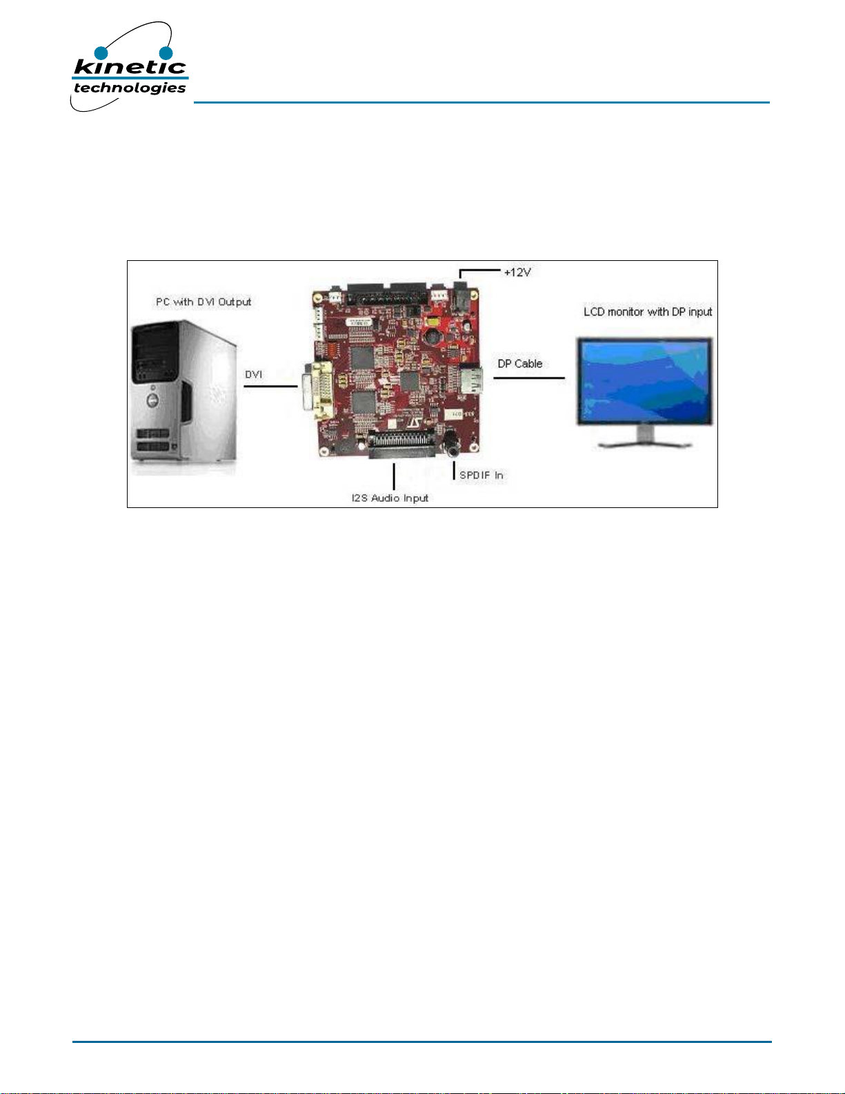
The picture below is a connection diagram showing the RD1-4028 board used for transferring a PC DVI signal
into a DisplayPort stream. This board uses the standard DisplayPort connector recommended in the DP 1.1a
specification to connect the DisplayPort output from the board to the input of the DisplayPort monitor.
1.
Connect the DVI output from a PC source to the RD1-4028 reference board using a DVIcable.
2.
Connect the output to a DisplayPort monitor using a DP cable. The RD1-4028 boardsupports
both single link and dual link DVI.
3.
Connect the 12 V (4A) DC power brick supplied for powering the board. An external digitalaudio
(I2S or SPDIF) source is recommended for testing digital audio conversion by the STDP4028
device into DisplayPort output.
4.
Once the connection is established, power ON the PC, monitor, RD1-4028 (DP transmitter)
board. An image should pop up on the screen within 5-6 seconds.
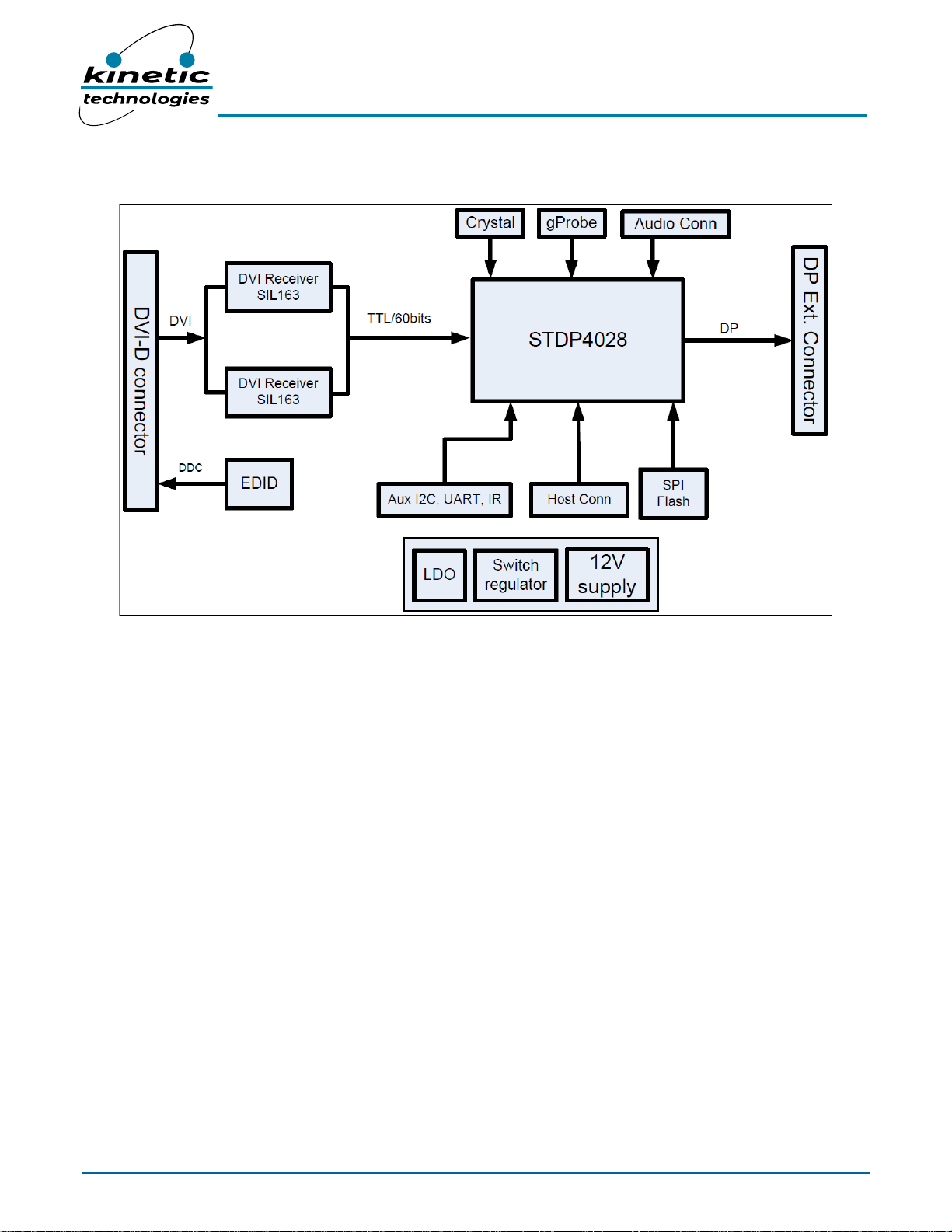
Note: The default configuration is dual bus TTL (dual link DVI) video input and SPDIF audio in. For single bus
TTL input (single link DVI), change the bootstrap setting Boot[5] to GND (populate R510 and remove
509). STDP4028 register setting changes are required in order to receive audio on I2S input. This can
be done through I2C host configuration or through firmware changes.
The RD1-4028 supports video resolution from 640 x 480 up to 2560 x 1600 and audio up to 8 Ch.
2.1.1.
I2C Host Port
Host connector (CN901) allows configuration of the STDP4028 IC from an external host (microcontroller)
through conventional I2C interface. User can plug two wires into pin 5 and pin 6 of this connector to access
the I2C port of the chip. STDP4028 default device ID is 0xE6/0xE7, but can be changed through bootstrap
settings. Refer to the STDP4028 datasheet for further details.
Figure 1. Connection Diagram: PC DVI Signal to DP Stream

X Reference Design Eval Kit
STDP4028-RD1
March 2020 –Revision 03a (Rev. B) Page 6 of 16 Company Confidential
2.1.2.
In-System Programming (ISP)
RD1-4028 uses SPI Flash to store the firmware. In case of a new firmware upgrade, the following method should
be used.
•
ISP through UART connector: Allows programming the SPI Flash through UART (RS232)
connector. Requires GProbe board (RS232 converter circuit) and GProbe software tool (contact
Kinetic).
2.1.3.
Diagnosis
If the image does not come up, follow the steps below for diagnosis.
Note: The diagnosis requires the Kinetic GProbe software and hardware tool. Contact Kinetic for the
GProbe software and board.
1.
Install the GProbe diagnostic tool on a computer and set the baud rate to 115,200.
2.
Connect GProbe board (not supplied) to the serial port (or USB port if using USB version) ofthe
computer.
3.
Connect the other end of the GProbe board to connector (CN902) on the RD1-4028 boardusing 4-
wire cable (part of the GProbe board).
Note: CHECK POLARITY while connecting the cable; Pin 1 is marked on the board. The 4-wirecable
connection from CN504 to GProbe board is 1 to 1.
4.
Hit the Reset button on the board (RESET SW901). You will see the firmware version and date of
firmware in the GProbe window. This indicates the DP receiver IC is functional. If the message
does not appear, reprogram the Flash using the ISP method described in the GProbe userguide.
5.
Using an oscilloscope, check the video input and output from the STDP4028.
Note: Refer to the STDP4028 datasheet for pinout descriptions.

X Reference Design Eval Kit
STDP4028-RD1
March 2020 –Revision 03a (Rev. B) Page 7 of 16 Company Confidential
3.
Board Description
Figure 2. Block Diagram

X Reference Design Eval Kit
STDP4028-RD1
March 2020 –Revision 03a (Rev. B) Page 8 of 16 Company Confidential
Figure 3. Board Picture

X Reference Design Eval Kit
STDP4028-RD1
March 2020 –Revision 03a (Rev. B) Page 9 of 16 Company Confidential
3.1. Principal Components and Functions
Below is a summary of all necessary connectors, switches, and other components. Please refer to the latest
board schematics for further details.
Table 3.1-1. Principal Components and Functions
Label
Description
RefDes
Power Input
(+12V)
Input 12 V, down conversion to 5 V, 3.3 V, and 1.2 V. This board uses a switch
regulator for 5 V and an LDO [low- dropout] for 3.3 V and 1.2 V. Note the analog and
digital supplies (3.3A and 3.3D or 1.2A and 1.2D) are isolated using ferrite beads.
CN301
STDP4028
The STDP4028 is capable of receiving and converting LVTTL video and I2S (or
SPDIF) audio input into a DisplayPort output. This device offers LVTTL input interface
configurable to map a wide range of display controller products. The 60-bit LVTTL
input ports on STDP4028 can be mapped to transfer video data either in two pixels
per clock or single pixel per clock of a chosen color depth.
U601
DP Output
DisplayPort output connector
CN801
Flash
The board includes an SPI Flash of 2 MB to hold the firmware. The SPI Flash can be
programmed (ISP) through UART interface
U602
DVI In
DVI Input connector
CN401
Sil163
DVI Receivers: The 48-bit TTL video output from DVI receivers are connected to the
STDP4028. By default, DVI input is configured for a single link operation up to 165
MHz. In this case, both transmitters are operating at half the clock rate. A custom
configuration is required for handling higher speed signals, such as WQXGA resolution.
(Contact your local Kinetic FAE for support.)
U401 U402
Digital Audio
Input
The I2S (8 channel) or S/PDIF (single wire, 3.3 V) audio input signals from the
external audio Codec card are received by CN903.
CN903
Analog S/PDIF
Input
Standard S/PDIF input connector.
CN904
Host Interface
Host Interface (I2C): This board includes a provision to access the STDP4028 device
from an external host controller through the Host Interface (I2C port) connection.
CN901
GProbe
GProbe Interface (+3.3V logic): the board also includes a GProbe connector that
connects to the STDP4028 UART port for communication with external PC sources for
debug purposes. The Kinetic GProbe tool (software) and PC serial port interface board
together create a debug environment for device debug and firmware update. The
GProbe interface is also used for ISP purposes.
CN902
Reset
Reset Button, when pressed, triggers a system master reset through the internal reset
circuitry. The reset button is used for system reset and debugging purposes and is not
required for production board design as the STDP4028 produces an internal reset
during power ON.
SW901
IR Input
An IR connector for interfacing the IR receiver.
CN601
AUX_I2C
A simplified connector for Host Interface debug
CN602
AUX_UART
UART Interface (for UART-over-Aux testing)
CN603
LED
Single LED for indicating the power on status.
D301
EDID
EDID Option: Currently not populated to allow pass through.
U604
Crystal
An external crystal of 27 MHz. The design makes use of internal oscillator circuitry.
X601
ESD Diodes
ESD protection diodes for DisplayPort signal (main lanes, AUX, and HPD line). The
board implements low cost ESD diodes.
ESD801
ESD802
ESD803
ESD804
SW902
Switches UART between Host Interface & GProbe Interface (see mark on PCB).
SW902

X Reference Design Eval Kit
STDP4028-RD1
March 2020 –Revision 03a (Rev. B) Page 10 of 16 Company Confidential
Table 3.1-2. Principal Components and Functions (continue)
Label
Description
RefDes
DVI Config
The RD1-4028 board has a switch for DVI transmitter hardware configuration. The
switch SW401 controls DVI Receivers U401 and U402. The switch position is logic
HIGH, which is set for dual pixel input mode of operation with rising edge data
sampling. The switch definitions are described in section 4.3.
SW401
Bootstrap
Options
The bootstrap options can be configured for:
−IROM/SPI Flash
−Single/Dual TTL
Refer to the datasheet for more details.
R503
R504
R509
R510
3.2. Connector Descriptions
The RD1-4028 has the following connectors. The locations of these connectors are shown in the board picture
in Figure 3.
CN301 –+12V DC 4A Power Input Jack
CN902 –GProbe Interface (4x1 pin keyed header) connects to the UART port of the STDP4028. Use the Kinetic
GProbe board and interface cable for connecting the board to an external PC that has GProbe software running.
Pin 1
+5V
Pin 2
GPROBE_TX
Pin 3
GPROBE_RX
Pin 4
GND

X Reference Design Eval Kit
STDP4028-RD1
March 2020 –Revision 03a (Rev. B) Page 11 of 16 Company Confidential
CN901 –I2C Host Interface (header 17X2) connector for connecting external host. This is used only when
an external host controller accesses the DisplayPort transmitter; not used for normal operation. In normal
operation, internal MCU controls the overall functioning of the DisplayPort Transmitter (refer to the
schematics for complete pin description for the Host Interface).
Pin 1 & 2
+5V
Pin 3 & 4
GND
Pin 5
AUX_I2C_SCL
Pin 6
AUX_I2C_SDA
Pin 7
HOST_TX
Pin 8
HOST_RX
Pin 9
RESET from Host
Pin 10
NC
Pin 11 & 12
GND
Pin 13
AUX_UART_TX
Pin 14
AUX_UART_RX
Pin 15
I2C_SCL
Pin 16
I2C_SDA
Pin 17 &18
NC
Pin 19 & 20
GND
Pin 21 & 22
NC
Pin 23
IRQ/BOOT7
Pin 24
IR_IN
Pin 25 & 26
NC
Pin 27 & 28
GND
Pin 29
GPIO_3/BOOT6
Pin 30
GPIO_0/BOOT3
Pin 31
TP901
Pin 32
GPIO_1/BOOT2
Pin 33
TP902
Pin 34
GPIO_2/BOOT5

X Reference Design Eval Kit
STDP4028-RD1
March 2020 –Revision 03a (Rev. B) Page 12 of 16 Company Confidential
CN801 –DisplayPort connector. Pin out details are shown below.
Pin 1
ML_Lane 0(p)
Pin 2
GND
Pin 3
ML_Lane 0 (n)
Pin 4
ML_Lane 1 (p)
Pin 5
GND
Pin 6
ML_Lane 1 (n)
Pin 7
ML_Lane 2 (p)
Pin 8
GND
Pin 9
ML_Lane 2 (n)
Pin 10
ML_Lane 3 (p)
Pin 11
GND
Pin 12
ML_Lane 3 (n)
Pin 13
GND
Pin 14
GND
Pin 15
AUX_CH (p)
Pin 16
GND
Pin 17
AUX_CH (n)
Pin 18
Hot Plug Detect
Pin 19
Return (GND)
Pin 20
DP_PWR
Pin 11
GND

X Reference Design Eval Kit
STDP4028-RD1
March 2020 –Revision 03a (Rev. B) Page 13 of 16 Company Confidential
CN401 –DVI-D input dual link DVI connector. Pin out description for the DVI connector is shown below.
Pin 1
RX2-
Pin 2
RX2+
Pin 3
GND
Pin 4
S_RX1-
Pin 5
S_RX1+
Pin 6
DVI_SCL
Pin 7
DVI_SDA
Pin 8
NC
Pin 9
RX1-
Pin 10
RX1+
Pin 11
GND
Pin 12
S_RX0-
Pin 13
S_RX0+
Pin 14
DVI_+5V
Pin 15
GND
Pin 16
+5V
Pin 17
RX0-
Pin 18
RX0+
Pin 19
GND
Pin 20
S_RX2-
Pin 21
S_RX2+
Pin 22
GND
Pin 23
RXC+
Pin 24
RXC-
Pin C1 through C5
NC

X Reference Design Eval Kit
STDP4028-RD1
March 2020 –Revision 03a (Rev. B) Page 14 of 16 Company Confidential
CN904 –SPDIF Input connector. The pin out description is shown below.
Pin 1
GND
Pin 2
I2S_0
Pin 3
GND
CN903 –I2S Digital Audio Input (52 pin) connector.
Pin A1
NC
Pin A2 & A3
GND
Pin A4 through A6
NC
Pin A7
GND
Pin A8 & A9
NC
Pin A10
I2S_3
Pin A11
I2S_2
Pin A12
I2S_1
Pin A13
NC
Pin A14
I2S_0
Pin A15
DNP
Pin A16 & A17
GND
Pin A18 through A21
NC
Pin A22
I2S_BCLK
Pin A23
+5V
Pin A24
I2S_WCLK
Pin A25 & A26
+5V
Pin B1
GND
Pin B2 & B3
NC
Pin B4 & B5
GND
Pin B6 & B7
NC
Pin B8 & B9
GND
Pin B10 through B13
NC
Pin B14 & B15
GND
Pin B16 through B18
NC
Pin B19 & B20
GND
Pin B21
+12V
Pin B22
NC
Pin B23
+12V
Pin B24
NC
Pin B25
+12V
Pin B26
GND

X Reference Design Eval Kit
STDP4028-RD1
March 2020 –Revision 03a (Rev. B) Page 15 of 16 Company Confidential
CN602 –I2C Host Interface (similar to CN901 with four pin header only, simplified version for debug
purposes)
Pin 1
+5V
Pin 2
I2C_SCL
Pin 3
I2C SDA
Pin 4
GND
CN603 –UART Interface (for UART-over-Aux testing)
Pin 1
+5V
Pin 2
Aux_UART_TX
Pin 3
Aux_UART_RX
Pin 4
GND
3.3. Switches
DVI Configuration Switch (SW401): The RD1-4028 board has a switch for DVI transmitter hardware
configuration. The switch SW401 controls DVI Receivers U401 and U402. The switch position is logic HIGH,
which is set for dual pixel input mode of operation with rising edge data sampling. The switch definitions of
SW401 are described below.
SW
Name
Definitions
SW401.1
SW401.2
/OCK_INV
1: Inverted ODCLK
0: Normal ODCLK
SW401.3
SW401.4
ST
1: High Output Drive Strength
0: Low Output Drive Strength
SW401.5
PIXS/M_S
1: 2-pixel/clock when in single link
0: 1-pixel/clock when in single link
SW401.6
STAG_OUT
1: Normal Simultaneous Outputs (EVEN & ODD)
0: Staggered Output
Host Interface Switch (SW902): This switch selects the use of GProbe connector or Host Interface
connector.
SW901.1
HOST_TX
SW901.2
UART_TX
SW901.3
GPROBE_TX
SW901.4
HOST_RX
SW901.5
UART_RX
SW901.6
GPROBE_TX

X Reference Design Eval Kit
STDP4028-RD1
March 2020 –Revision 03a (Rev. B) Page 16 of 16 Company Confidential
3.4. Stuffing Options
3.4.1.
Single/dual bus TTL input
Single TTL configuration: stuff R510, unstuff R509
Dual TTL configuration: stuff R509, unstuff R510
3.4.2.
IROM/SPI-Flash
OCM boot from IROM code: stuff R504, unstuff R503
OCM boot from external ROM code: stuff R503, unstuff R504
Table of contents
Popular Media Converter manuals by other brands

Z3 Technology
Z3 Technology Z3-DME-01 User instructions

Rohm
Rohm BM2P10B1J-EVK-001 user guide

Puls
Puls CD10.241 installation manual

Southwestern Microsystems
Southwestern Microsystems Music-In-A-Flash MD-MIAF4 Installation and operation manual

Edimax
Edimax ET-912 Series Declaration of conformity

Siemens
Siemens SINAMICS G110M operating instructions