LG Industrial Systems GLOFA User manual

User’s Manual
LG Programmable Logic Controller
GLOFA
MASTER-K
LG Industrial Systems
G3F-DA4V
G3F-DA4I
G4F-DA1A

Be sure to read carefully the safety precautions given in data sheet and user’s manual before operating the module
and follow them.
The precautions explained here only apply to the G3F-DA4V, G3F-DA4I and G4F-DA1A(hereafter, called D/A con-
version module)
For safety precautions on the PLC system, see the GLOFA GM3/4 User’s Manuals and the MASTER-K200S/300S/
1000S CPU User’s Manuals.
A precaution is given with a hazard alert triangular symbol to call your attention, and precautions are represented
as follows according to the degree of hazard.
However, a precaution followed with can also result in serious conditions.
Both of two symbols indicate that an important content is mentioned, therefore, be sure to observe it.
Keep this manual handy for your quick reference in necessary.
SAFETY PRECAUTIONS
WARNING
!
If not provided with proper prevention, it can cause death or fatal
injury or considerable loss of property.
CAUTION
!
If not properly observed, it can cause a hazard situation to result
in severe or slight injury or a loss of property.
CAUTION
!
CAUTION
!
Design Precautions
▶
Design a safety circuit in the outside of the PLC for system safety in
case of disorder of the external power or PLC module body. Other-
wise, it can cause injury due to wrong output or malfunction.
1) The following shows analog output states according to various
settings of functions that control analog output. When setting an
output state, be cautious for safety. Channel SpecificationChannel Setting
State Used Unused
PLC CPU in RUN state. A D/A conversion
value is output.
PLC CPU in STOP state
PLC CPU in Error state
Communication error of
the remote I/O station
(When loaded on the
remote I/O station)
A value of the speci-
fied output state will
be output.
0: Median value of the
outputrange
1: Previous value
2: Max. value of the
outputrange
3: Min. value of the
outputrange
Voltage:
0 V
Current:
12 mA
2) Sometimes, fault of output device or internal circuit can make
output abnormal. Design a supervising circuit in the outside for
output signals which can cause serious accidents.
CAUTION
!
▶
Do not run I/O
signal lines near
to high voltage
line or power line.
Separate them as
100 mm or more
as possible. Oth-
erwise, noise can
cause module
malfunction.

WARNING
!
Test Run and Maintenance
Precautions
▶Do not contact the terminals
while the power is applied.
It can cause malfunction.
▶
When cleaning or driving a term
i-
nal screw, perform them after the
power has been turned off
▶
Do not perform works while the
power is applied, which can
cause disorder or malfunction.
CAUTION
!
▶
Do not separate the module from
the printed circuit board(PCB), or
do not remodel the module.
They can cause disorder, mal-
function, and damage
of the
module or a fire.
When mounting or dismounting
the module
, perform them after
the power has been turned off.
▶
Do not perform works while the
power is applied, which can
cause disorder or malfunction.
CAUTION
!
Waste Disposal Precautions
▶When disposing the module, do it as an industrial waste.
CAUTION
!
Installation Precautions
▶
Operate the PLC in the environ-
ment cond
itions given in the
generalspecifications.
▶If operated in other
environment
not specified in the general
specifications, it can cause an
electric shock, a fire, malfunction
or damage or degradation of the
module
▶
Make sure the module fixing
projectio
ns is inserted into the
module fixing hole and fixed.
▶Improper installation of the mod-
ule can cause malfunction, dis-
order or falling.
CAUTION
!
WiringPrecautions
▶When grounding a FG terminal,
be sure to provide class 3
grounding which is dedicated to
the PLC.
▶Before the PLC wiring, be sure to
check the rated voltage and ter-
minal arrangement for the mod-
ule and observe them correctly.
If a different power, not of the
rated voltage, is applied or
wrong wiring is provided, it can
cause a fire or disorder of the
nodule.
▶Drive the terminal screws firmly
tothedefinedtorque.
If loosely driven, it can cause
short circuit, a fire or malfunc-
tion.
▶
Be care
ful that any foreign matter
like wire scraps should not enter
into the module.
It can cause a fire, disorder or
malfunction.

◎
CONTENTS
◎
Chapter 1. INTRODUCTION
1.1 Features ············································································································································1 -1
1.1.1 G3F-DA4V G3F-DA4I···················································································································1 -1
1.1.2 G4F-DA1A·····································································································································1 -1
1.2 Glossary ············································································································································1 -2
1.2.1 A-Analog Value ·····························································································································1 -2
1.2.2 D-DigitalValue ····························································································································1 -2
1.2 3 Digital/AnalogConversion Characteristics ···················································································1 -3
Chapter 2. SPECIFICATIONS
2.1 General Specifications ····················································································································2 -1
2.2 Performance Specifications················································································································2 -2
2.3 Names of Parts and Functions ·······································································································2 -3
2.3.1 G3F-DA4V / G3F-DA4I ···············································································································2 -3
2.3.2 G4F-DA1A ································································································································2 -5
2.4 External Power Supply (
±
15 VDC Specifications)······································································2 -6
2.5 I/O Conversion Characteristics···········································································································2 -7
2.5.1 Offset/GainValue ························································································································2 -7
2.5.2 Example for I/O Conversion Characteristic ················································································2 -7
2.5.3 Relations between Offset/Gain Valueand Analog Output ·························································2 -8
2.5.4 I/O Conversion Characteristics According to theOffset/Gain Setting ········································2 -9
1) VoltageOutput Characteristics ··································································································2 -9
2) CurrentOutput Characteristics ·································································································2 -11
2.6 D/A Conversion Speed ··················································································································2-12
2.7 Offset/GainSetting·····························································································································2-12
2.7.1 Noteson Setting Offset/Gain Value····························································································2-13
2.7.2 Procedures of Setting Offset/Gain ··························································································2-14

Chapter 3. INSTALLATION AND WIRING
3.1 Installation·············································································································································3 -1
3.1.1 InstallationAmbience····················································································································3 -1
3.1.2 Installation Precautions·················································································································3 -1
3.2 Wiring ··················································································································································3 -2
3.2.1 Wiring Precautions························································································································3 -2
3.2.2 WiringExamples ·······················································································································3 -2
1) G3F-DA4V·······································································································································3 -2
2) G3F-DA4I ····································································································································3 -3
3) G4F-DA1A·······································································································································3 -3
3.3 Wiring between the G3F-DA4I or the G3F-DA4V and DC 15V ·························································3 -5
3.3.1 On Use of the G3F-PA1A or the G3F-PA2A·················································································3 -5
3.3.2 On Use of External Power Supply ······························································································3 -6
Chapter 4. FUNCTION BLOCK
4.1 Insertion of the Function Block for the D/A Conversion Module on the GMWIN··························4 -1
4.2 Local Function Block ······················································································································4 -2
4.2.1 Module Initialization ··················································································································4 -2
(G3F-DA4V / G3F-DA4I : DA4INI, G4F-DA1A : DA1INI)
4.2.2 Module Write_Array Type ···········································································································4 -3
(G3F-DA4V / G3F-DA4I:DA4AWR, G4F-DA1A : DA1AWR)
4.2.3 Module Write_Single Type············································································································4 -4
(G3F-DA4V / G3F-DA4I : DA4WR, G4F-DA1A : DA1WR)
4.3 RemoteFunction Block ·····················································································································4 -5
4.3.1 Module Initialization (G3F-DA4V / G3F-DA4I : DAR4INI, G4F-DA1A : DAR1INI)·······················4 -5
4.3.2 Module Write (G3F-DA4V / G3F-DA4I : DAR4WR, G4F-DA1A : DAR1WR)·······························4 -6
4.4 Errors on Function Block····················································································································4 -7
Chapter 5. GM PROGRAMMING
5.1 Programming for Controlling InverterSpeed with 5 Step Analog Output Voltage·······················5 -1
5.2 Programming for Displaying D/A Conversions whichisSet by Digital Switch ··························5 -6
5.3 Programming for Mounting D/A Conversion Module on Remote I/O Station ·····························5 -9

Chapter 6. BUFFER MEMORY CONFIGURATION AND FUNCTION
6.1 Buffer Memory Configuration ···········································································································6 -1
6.1.1 G3F-DA4V / G3F-DA4I ···············································································································6 -1
6.1.2 G4F-DA1A ································································································································6 -2
6.2 Buffer MemoryFunction······················································································································6 -3
6.2.1 Available ChannelSpecification ·······························································································6 -3
6.2.2 DataInput Type Specification·······································································································6 -3
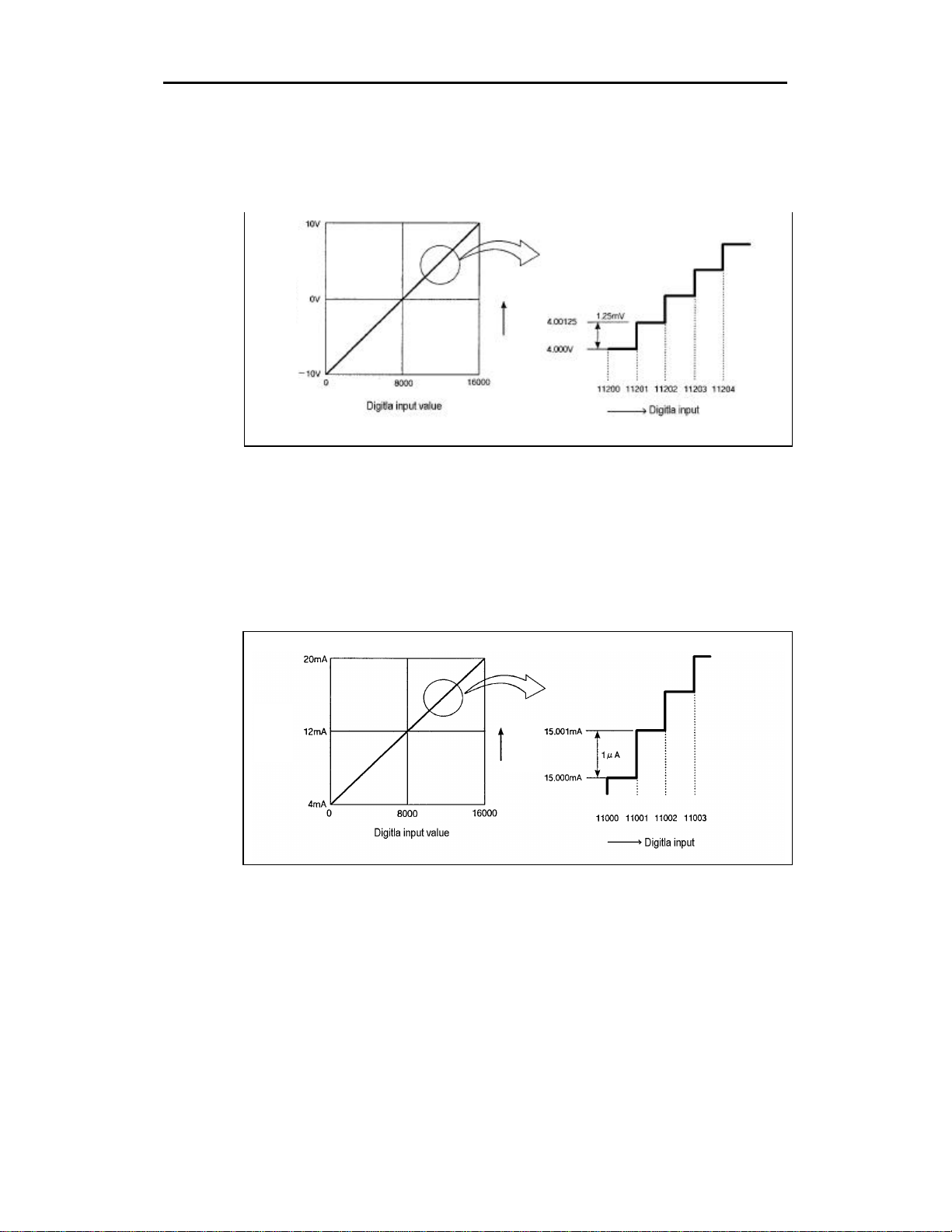
6.2.3 Digital Input ·································································································································6 -4
6.2.4 Specification of CPUModule's Stop Conditionor Disabled Channel's OutputCondition············6 -4
6.2.5 SET DataSpecification ···············································································································6 -5
6.2.6 ChannelOperation Data Area······································································································6 -5
Chapter 7. SPECIALMODULECOMMAND(BUFFER MEMORYREAD/WRITE)
7.1 Local Command···································································································································7 -1
7.1.1 BufferMemory Read-GET, GETP Command ············································································7 -1
7.1.2 Buffer Memory Write-PUT, PUTP Command ··········································································7 -2
7.2 Remote Command································································································································7 -3
7.2.1 Buffer Memory Read-RGET ······································································································7 -3
7.2.2 BufferMemory Write-RPUT ····································································································7 –4
Chapter 8. MK PROGRAMMING
8.1 Basic Programming ·························································································································8 -1
8.1.1 G3F-DA4V / G3F-DA4I ················································································································8 -1
8.1.2 G4F-DA1A ································································································································8 -2
8.2 Application Programming ···············································································································8 -3
8.2.1 Programming for Controlling InverterSpeed with 5 Step Analog Output Voltage·······················8 -3
8.2.2 Programming for Displaying of D/A Conversions which is Set byDigital Switch ····················8 -5
8.2.3 Programming for Mounting D/A Conversion Module on RemoteI/O Station ····························8 -7
Chapter 9. TROUBLESHOOTING
9.1 Error Code Indicated by RUN LED Flickering···················································································9 -1
9.2 Troubleshooting Procedure················································································································9 -1
9.2.1 RUNLEDFlickering ····················································································································9 -1
9.2.2 RUNLEDOff ····························································································································9 -2
9.2.3 SuddenD/A OutputValue Change·······························································································9 -3

9.2.4 Digital and Analog Value Mismatch······························································································9 -4
9.2.5 D/A Output Value Always deviates from Specified Value·····························································9 -5
9.2.6 AnalogOutputValueAccording to D/A Input Valueisn'tChanged ··············································9 -6
9.2.7 D/AConversion Module HardwareFault ····················································································9 -6
Chapter 10. G3F-PA1A/G3F-PA2A POWER SUPPLY MODULE
10.1 Performance Specification ············································································································10 -1
10.2 Notes on Handling ·························································································································10 -2
10.3 NamesofParts ·······························································································································10 -2
10.4 Dimensions ····································································································································10 –3
Chapter 11. DIMENSIONS
11.1 G3F-DA4V / G3F-DA4I Dimensions ·····························································································11 -1
11.2 G4F-DA1A Dimensions ·················································································································11 -2

Chapter 1. INTRODUCION
1 -1
Chapter 1. INTRODUCTION
The G3F-DA4V, the G3F-DA4I and the G4F-DA1A are digital/analog conversion modules for use with the GLOFA
PLC GM 1/2/3/4 series CPU module and the MSTER-K300S/1000S series CPU module. The G4F-DA1A is used
on the GM4 series module and the K300S series module. the G3F-DA4V and the G3F-DA4I are used on the
GM1/2/3 series module and the K1000S series module. (Here-in-after the G4F-DA1A, G3F-DA4V and G3F-DA4I
are called the D/A conversion module)
The D/A conversion module is to convert a 16-bit, signed BIN digital value into an analogoutput signal (voltage or
current).
1.1 Features
1.1.1 G3F-DA4V / G3F-DA4I
1)Allows digital to Analog conversion for 16 channels per a module.
G3F-DA4V: 1 module can be performed for D/A conversion (voltage output) of 16 channels.
G3F-DA4I: 1 module can be performed for D/A conversion (current output) of 16 channels.
2) High resolution of 1/16000
A digital value resolution can be selected among 1/16000 and so the analog value of high resolution
iskept.
4)The number of the D/A conversion module mounted on one base is unlimited.
On use of power supply module of the G3F-PA1A or G3F-PA2A, the G3F-DA4V and G3F-DA4I can
be mounted up to 4.
1.1.2 G4F-DA1A
1)Allows digital to Analog conversion for 2 channels per a module.
1 module can be performed for D/A conversion (voltage or current output) of 2 channels.
2) High resolution of 1/16000
A digital value resolution can be selected among 1/16000 and the analog value of high resolution is
kept.
3)The number of the G4F-DA1A mounted on one base is unlimited.

Chapter 1. INTRODUCION
1 -2
1.2 Glossary
1.2.1 A-Analog Value
Analog value is a sequentially changing value such as voltage, current, temperature, speed, pressure,
flux, etc.
Temperature, for example, is sequentially changing according to the time. Because this temperature is
not input on the PLC directly, the same analog value of DC voltage (0 to ±10V) or current (4 to 20mA)
inaccordance with the temperature should be input on the PLC through transducer.
1.2.2 D-Digital Value
Digital value is non-sequentially changing value written
as the number like 0, 1, 2, 3. The signal of on or off is
written as digital value of 0 or 1. There are BCD value
and binary value in the range of digital value.
Analog value isn't written directly on the CPU. For
analog input to the CPU operation, analog converted
to digital value has to be input on the CPU. and for
analog output, the digital of CPU should be
converted to analog.
Numberofman
time
[Fig. 1.3] Digital quality
A/D
Conversion
CPU
(Digital
processing)
D/A
Conversion
Analog
0~±10V or
4~20mA
Analog
0~±10Vor
4~20mA
[Fig. 1.4] conversion processing
in the PLC
0
Temperature
time
[Fig 1.1] Analog Value [Fig 1.2] Example of Transducer
Temperature
0 ~ 1000°C
Transducer
-10 ~ 10V
voltage input to
A/Dconversion
module
⇒
⇒

Chapter 1. INTRODUCION
1 -3
1.2.3 Digital/Analog Conversion Characteristics
1)Voltageoutput
[Fig 1.5] D/A conversion characteristics(Voltage output)
Digital/analog conversion module allows digital value of the CPU to be converted intoan analog value
and to be output externally. Digital input value of 0 leads to analog output value of -10V and 16000
leads to 10V. Digital input value of 1 is equal to 1.25mV.
2)Currentoutput
[Fig 1.6] D/A conversion characteristics(Current output)
On current output, digital value of 0 is to be converted into 4mA and 16000.into 20mA. Digital input of 1
is equal to 1㎂.
Analog
output
current
Analog
output
current
Analog
output
voltage
Analog
output
voltage

Chapter 2. SPECIFICATIONS
2 -1
Chapter 2. SPECIFICATIONS
2.1 General Specifications
Table 2.1 shows the common specifications of GLOFA GM series and MASTER-Kseries
No ItemsSpecificationsReference
Specification
1Operatingambient
temperature 0 ~ 55℃
2Storage ambient
temperature-25 ~ 75℃
3Operatingambient
humidity 5 ~ 95%RH, non-condensing
4Storage ambient
humidity 5 ~ 95%RH, non-condensing
Occasional vibration
Frequency Acceleration Amplitude Sweep count
10≤f∠57 Hz
-
0.075mm
57
≤
f
≤
150 Hz
9.8 m/s2{1G}-
Continuous vibration
Frequency
Acceleration
Amplitude
10
≤
f
∠
57 Hz
-
0.035mm
5Vibration
57
≤
f
≤
150 Hz
4.9 m/s2{0.5G}
-
10 timesin
eachdirection
for X, Y, Z
IEC 61131-2
6Shocks•Maximum shock acceleration: 147 m/s2{15G}
•Duration time :11ms
•Pulse wave: half sine wave pulse( 3 timesin eachof X, Y and Z directions ) IEC 61131-2
Square wave impulse noise ±1,500V
Electrostaticdischarge Voltage :4kV(contact discharge) IEC 61131-2
IEC 1000-4-2
Radiated
electromagnetic field 27 to 500 MHz, 10V/m IEC 61131-2
IEC 1000-4-3
Severity
Level All power
modulesDigital
I/Os(U
e≥
24 V)
DigitalI/Os
(Ue < 24 V)
Analog/Os
communication
I/Os
IEC 61131-2
IEC 1000-4-4
7Noise immunity
Fast transient /burst noise
Voltage
2kV
1kV
0.25kV
8
Operating
atmosphere
Free from corrosive gases and excessive dust
9
Altitude for use
Up to2,000m
10
Pollution degree
2 or lower
11
Cooling method
Self-cooling
[Table 2.1 ] General Specifications
REMARK
1) IEC(InternationalElectrotechnicalCommission)
:The international civilian organization which produces standards for electrical and electronics industry..
2) Pollutiondegree
:It indicates a standard of operating ambient pollution level.
The pollution degree 2 means the condition in which only non conductive pollution occurs. Occasionally,
however, a temporary conductivity caused by condensation shall be expected.

Chapter 2. SPECIFICATIONS
2 -2
2.2 Performance Specifications
Table 2..2 shows performance specification of D/A conversion module.
Specifications
ItemsG3F-DA4I G3F-DA4V G4F-DA1A
I/O points 16points
Digital input •16bit(data part :14bits)signed binary
•May be set per channel by setting input data.("0" : -192~16191, "1" :-8192~-8191)
Analog output DC 4~20mA
(Externalloadresistance
less than 510Ω)
-5~5VDC
(Externalloadresistance:2KΩ~
1MΩ)
-10~10VDC
(Externalloadresistance:2KΩ~
1MΩ)
-5~5VDC
(Externalloadresistance:
2KΩ~1MΩ)
DC-4~20mA
(Externalload resistance less
than550Ω)
Max.resolution 1μA(1/16000)
-5~5VDC
0.625mV(1/16000)
-10~10VDC
1.25 mV(1/16000)
-10~10VDC
1.25mV(1/16000)
DC4~20 mA:
1μA(1/16000)
Accuracy ±0.3% [Full Scale]
Max. conversion
speed (ms/channel)
15ms/16channels 3ms/ 2channels
Max.absoluteinput DC 24mA 15VDC
Voltage: 15 VDC
Current:DC 24mA
Analogoutputpoints 16 channels/1module 2channels/1module
Isolation Between input terminals and the PLC: Photo-coupler isolation
Terminalsconnected
consumption 38-point terminalblock 20-pointterminalblock
Internalcurrent
ccconsumption
0.25 A0.45 A
Voltage 15VDC/-15VDC
External
power supply Current 15 VDC : 0.5 A
-15 VDC : 0.1 A 15VDC:0.5A
-15 VDC:0.3A-
Weight 610 g630 g370 g
[Table 2.2] Performance Specifications

Chapter 2. SPECIFICATIONS
2 -3
2.3 Names of Parts and Functions
Names of parts and functions are shown as below.
2.3.1 G3F-DA4V/ G3F-DA4I
②
④
⑤
4~20mA

Chapter 2. SPECIFICATIONS
2 -4
No.Descriptions
RUNLED
①Indicates the operating condition of the D/A conversion module
* On:Normal operation
* Flickering: An error has occurred. (For more information, see the Section 6.1)
* Off : 5 VDC power off or D/A conversion module fault
Channel select switch
②Used to set the channel of the adjustment of offset/gain in the test mode.
Setting range: 0~F
Offset/gainselectswitch
③
Used to select Offset/Set/Gain .
*Offset position: offset value adjustment mode
*Gain position: gain value adjustment mode
*Set position: the mode which stores offset/gain value.
(When the switch is changed to "set" position from "Offset/ Gain" position, offset/gain value
is stored in the memory of D/A conversion module.)
Up/Down switch
④
-Used to make microadjustment of offset/gain value.
-Analog output value according to up/down locationischangedasfollows.:
*Up/down location of less than 2 sec : G3F-DA4I-Add or fall of 1㎂/1time
G3F-DA4V-Add or fall of 1.25 mV/1 time
*Up/down location of more than 2 sec : G3F-DA4I-Add or fall of 10㎂/ 0.2 sec.
G3F-DA4V Add or fall of 12.5 mV/0.2 sec
Test terminal block
⑤Test mode is to be a connection of terminal block 1 and 2
Normal mode is to be a disconnection of terminal block 1 and 2
Output range select switch
⑥
It's only for the G3F-DA4V.
*Factory set is made to -10
~
10VDC.

Chapter 2. SPECIFICATIONS
2 -5
2.3.2 G4F-DA1A
No.Descriptions
RUNLED
①
Indicatestheoperating status the G4F-DA1A
*Normal mode
-On: Normal operation
-Flicker: error occurring
-Off: 5 VDC power off or the G4F-DA1A module fault.
*Test mode
-Flicker(per 1.0 sec): Offset/Gain select switch is set to offset
condition or gain condition.
-Off: offset/gain select switch is settoSetcondition.
Offset/ Set/Gainselectswitch
②
*Offset position: Offset value control mode
*Gain position: Gain value control mode
*Set position: Offset/Gain value set mode
(When offset/gain position is changed to set position,
offset/gain value is stored onto G4F-DA1A buffer
memory.)
Channelselectswitch
③
Used to select channel for adjusting offset/gain value on test mode.
*CH0:enabledto adjusttheoffset/gain value on the CH0
*Neutral: disabled to adjustthe offset/gain value
*CH1 :enabled to adjust the offset/gain value on the CH1.
Up/Down switch
④
-Used to make micro adjustment of offset/gain value.
-
Analog output value according to up/down location is changed as
follows.:
*Up/Down location of less than 2 sec Add or fallof1.25mA(voltage)
Add or fall of 1.0μA(current)
*Up/D
own location of more than 2 sec Add or fall of
12.5mA(voltage) Add or fall of 10μA(current)
Test terminal block
⑤
Test mode is to be a connection of terminal block 1 and 3
Normal mode is to be a disconnection of terminal block 1 and 3

Chapter 2. SPECIFICATIONS
2 -6
2.4 External Power Supply(
±
15 VDC Specifications)
Be sure to use rated power supply on the table 2.3when power(±15 VDC) is supplied to D/A conversion
module for use with the GLOFA PLC GM1/2/3 series and the MASTER-K1000S series.
Specifications
Item G3F-DA4I G3F-DA4V
+15VDC ±3%(14.55 V~15.45V)
Voltage -15 VDC ±3%(-15.45V~-14.55V)
+15 VDC 0.5 A 0.5 A
*1
Current consumption -15 VDC 0.1 A 0.3 A
Ripple voltage less than 50 mVp-p
Spikevoltage less than 100 mVp-p
transient output change lessthan±1V
[Table 2.3]External power supply specifications
*1: Current consumption shown on the above table 2.3 is applicable to a piece of D/A conversion module.

Chapter 2. SPECIFICATIONS
2 -7
2.5 Input/Output Conversion Characteristics
I/O characteristics are displayed as a slant of the line connecting offset value and gain value in converting an
digital signal from the external PLC into an analog signal(voltage or current).
The I/O conversion characteristics of the D/A conversion module are shown.
2.5.1 Offset/ Gain Value
1)Offset and gain value is as follows
a)Offsetvalue
Data formatof -8192~8191: When digital input value is -8000, offset value is analog output value.
Dataformatof -192~16191: When digital input value is 0, offset value is analog output value.
b)Gain value
Dataformatof -8192~8191: When digital input value is 0, offset value is analog output value.
Dataformatof -192~16191: When digital input value is 8000, offset value is analog outputvalue.
2)Factory set value of offset and gain value is like table 2.4.
Module name Analog input range Offset value Gain value
G3F-DA4I DC 4~20 mA DC4mA DC 12 mA
G3F-DA4V -10 ~10 VDC -10 VDC 0 VDC
G3F-DA1A -10 ~10 VDC -10 VDC 0 VDC
[Table 2.4] Factory set value of offset and gain
3)Offset and gain value can be selected per channel on test mode.
2.5.2 Examplefor I/OConversionCharacteristic.
Input/ output conversion characteristic example is shown on Fig 2.1
[Fig 2.1] Input/ output conversion characteristic example

Chapter 2. SPECIFICATIONS
2 -8
2.5.3 Relations between Offset/ Gain Value andAnalog Output
The resolution of D/A conversion module can be changed by changing offset/ gain value. At the change of
offset/ gain value, the below formula can calculate resolution of analog value and analog output value by
digitalinput value.
Gain value -Offsetvalue
Resolution =
8000
Gain value -Offsetvalue
Analog output = 5Digital input value +Offsetvalue
8000
Analog output = Resolution 5Digital input value 5Offsetvalue
Ex) Gain value : 0 VDC Offset value : -10 VDC Digital input value : 12000
0 –(-10)
Resolution = = 0.00125
8000
Analog output = 0.00125 512000 +(- 10) = 5(V)
Since maximum resolution of D/A conversion module is like values on table2.5, if digital input value increase
or decrease one at a time, analog output value may be different with a result of above formula
Product code Analog output range Maximum resolution
G3F-DA4I DC 4~20 mA 1μA
-10 ~10 VDC 1.25 mV
G3F-DA4V -5 ~5 VDC 0.625mV
DC 4~20 mA 1μA
G4F-DA1A -10 ~10 VDC 1.25 mV
[Table 2.5] Maximum resolution

Chapter 2. SPECIFICATIONS
2 -9
2.5.4 I/OConversionCharacteristics according to Offset/Gain Setting
Input/output conversion characteristics according to offset/ gain setting are as below.
1)Voltage outputcharacteristics
Voltage output characteristics according to offset/ gain setting are shown in the Fig2.2 and Fig2.3.
(1) -10 ~10 VDC
-10 ~10 VDC
[Fig 2.2] Voltage output characteristics(-10 ~ 10 VDC)
Digital input value
No Digital
Input
range
Offset
value Gain
value -8000 -4000 04000 8000 12000 16000
0 V 5 V --0 V 2.5 V 5 V 7.5 V 10 V
-5 V 0 V ---5 V -2.5 V 0 V 2.5 V 5 V
-192
~
16191 -10 V 0 V ---10 V -5 V 0 V 5 V 10 V
0 V 5 V 0 V 2.5 V 5 V 7.5 V 10 V --
-5 V 0 V -5 V -2.5 V 0 V 2.5 V 5 V --
-8192
~
8191 -10 V 0 V -10 V -5 V 0 V 5 V 10 V --
Analogoutputvoltage

Chapter 2. SPECIFICATIONS
2-10
(2) -5 ~ 5VDC
-5 ~5VDC
[Fig 2.3] Voltage output characteristics(-5 ~ 5VDC)
Digital input value
No Digital
Input
range
Offset
value Gain
value -8000 -4000 04000 8000 12000 16000
1 V 3 V --1 V 2 V 3 V 4 V 5 V
0 V 2.5 V --0 V 1.25V 2.5 V 3.75V 5 V
-192
~
16191 -5 V 0 V ---5 V -2.5 V 0 V 2.5 V 5 V
0 V 3 V 1 V 2 V 3 V 4 V 5 V --
1 V 2.5 V 0 V 1.25V 2.5 V 3.75V 5 V --
-8192
~
8191 -5V 0 V -5 V -2.5 V 0 V 2.5 V 5 V --
Analogoutputvoltage
This manual suits for next models
4
Table of contents
Other LG Industrial Systems Controllers manuals
Popular Controllers manuals by other brands

MR
MR TAPCON 230 Quick reference guide

ESYLUX
ESYLUX ELC SmartDriver Series Detailed operating instructions

Wilkerson
Wilkerson Dial-Air RRP-95-152 manual

EUTECH INSTRUMENTS
EUTECH INSTRUMENTS ALPHA CON 1000 CONDUCTIVITY... instruction manual

Texas Instruments
Texas Instruments TMS320DM646 Series user guide

Mitsubishi
Mitsubishi A1SJH(S8) user manual