- 9 - LGE Internal Use OnlyCopyright © 2010 LG Electronics. Inc. All rights reserved.
Only for training and service purposes
4. Manual Adjustment
4.1. ADC(GP2) Adjustment
4.1.1. Overview
ADC adjustment is needed to find the optimum black level and
gain in Analog-to-Digital device and to compensate RGB
deviation.
4.1.2. Equipment & Condition
1) Adjust Remocon
2) 801GF(802B, 802F, 802R) or MSPG925FA Pattern Generator
- Resolution :
480i, 720*480 (MSPG-925FA -> Model: 209, Pattern: 65)
- 480i
1080p, 1920*1080 (MSPG-925FA -> Model: 225, Pattern:
65) - 1080p
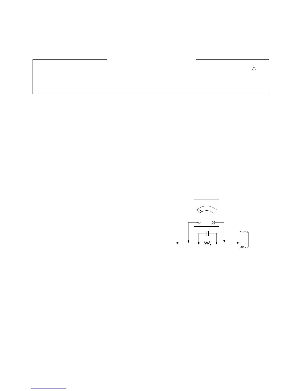
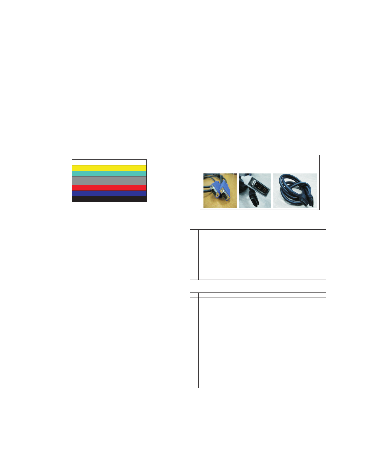
- Pattern : Horizontal 100% Color Bar Pattern
- Pattern level: 0.7 ± 0.1 Vp-p
- Image
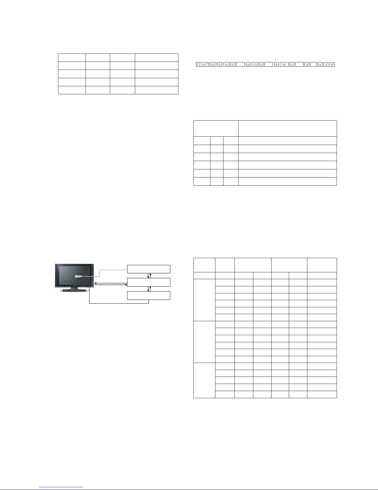
3) Must use standard cable
4.1.3. Adjust method
(1) ADC 480i, 1080p Comp1
1) Check connected condition of Comp1 cable to the equipment
2) Give a 480i, 1080p Mode, Horizontal 100% Color Bar
Pattern to Comp1.
(MSPG-925FA -> Model: 209, Pattern: 65) - 480i
(MSPG-925FA -> Model: 225, Pattern: 65) - 1080p
3) Change input mode as Component1 and picture mode
as “Standard”
4) Press the In-start Key on the ADJ remote after at least 1
min of signal reception. Then, select 7. External ADC ->
1. COMP 1080p on the menu. Press enter key. The
adjustment will start automatically.
5) If ADC calibration is successful, “ADC RGB Success” is
displayed. If ADC calibration is failure, “ADC RGB Fail” is
displayed.
6) If ADC calibration is failure, after recheck ADC pattern or
condition retry calibration Error message refer to 5).
(2) ADC 1920*1080 RGB
1) Check connected condition of Component & RGB cable
to the equipment.
2) Give a 1920*1080 Mode, 100 % Horizontal Color Bar
Pattern to RGB port.
(MSPG-925 Series -> model: 126 , pattern: 65 )
3) Change input mode as RGB and picture mode as
“Standard”.
4) Press the In-start Key on the ADJ remote after at least 1
min of signal reception. Then, select 7. External ADC ->
1. COMP 1080p on the menu. Press enter key. The
adjustment will start automatically.
5) If ADC calibration is successful, “ADC RGB Success” is
displayed. If ADC calibration is failure, “ADC RGB Fail” is
displayed.
6) If ADC calibration is failure, after recheck ADC pattern or
condition retry calibration Error message refer to 5).
4.2. EDID(The Extended Display Identification
Data)/DDC(Display Data Channel) download
(1) Overview
It is a VESA regulation. A PC or a MNT will display an
optimal resolution through information sharing without any
necessity of user input. It is a realization of “Plug and Play”.
(2) Equipment
- Adjust remote control
- Since embedded EDID data is used, EDID download JIG,
HDMI cable and D-sub cable are not need.
(3) Download method
1) Press Adj. key on the Adj. R/C, then select “10.EDID
D/L”, By pressing Enter key, enter EDID D/L menu.
2) Select [Start] button by pressing Enter key, HDMI1 /
HDMI2 / HDMI3 / HDMI4 / RGB are Writing and display
OK or NG.
(4) EDID DATA
AHDMI
ARGB
AReference
- HDMI1 ~ HDMI4 / RGB
- In the data of EDID, bellows may be different by S/W or
Input mode.
D-sub to D-sub DVI-D to HDMI or HDMI to HDMI
For HDMI EDIDFor Analog EDID
0 123456789ABCDEF
0 00FFFFFFFFFFFF001E6D01 0001 01 01 01
10 01 14 01 03 68 10 09 78 0A EE 91 A3 54 4C 99 26
20 0F 50 54 A1 08 00 81 80 61 40 45 40 31 40 01 01
30 01 01 01 01 01 01 02 3A 80 18 71 38 2D 40 58 2C
40 45 00 A0 5A 00 00 00 1E 01 1D 00 72 51 D0 1E 20
50 6E 28 55 00 A0 5A 00 00 00 1E 00 00 00 FD 00 3A
60 3F 1E 53 10 00 0A 20 20 20 20 20 20 00 00 00 FC
70 00 4C 47 20 54 56 0A 20 20 20 20 20 20 20 00 1D
0123456789ABCDEF
0 00FFFFFFFFFFFF001E6D01 0001 01 01 01
10 01 14 01 03 80 10 09 78 0A EE 91 A3 54 4C 99 26
20 0F 50 54 A1 08 00 71 4F 81 01 01 01 01 01 01 01
30 01 01 01 01 01 01 02 3A 80 18 71 38 2D 40 58 2C
40 45 00 A0 5A 00 00 00 1E 01 1D 00 72 51 D0 1E 20
50 6E 28 55 00 A0 5A 00 00 00 1E 00 00 00 FD 00 3A
60 3F 1E 53 10 00 0A 20 20 20 20 20 20 00 00 00 FC
70 00 4C 47 20 54 56 0A 20 20 20 20 20 20 20 01 D7
80 02 03 26 F1 4E 10 1F 84 13 05 14 03 02 12 20 21
90 22 15 01 26 15 07 50 09 57 07 67 03 0C 00 XX XX
A0 B8 2D E3 05 03 01 01 1D 80 18 71 1C 16 20 58 2C
B0 25 00 A0 5A 00 00 00 9E 01 1D 00 80 51 D0 1A 20
C0 6E 88 55 00 A0 5A 00 00 00 1A 02 3A 80 18 71 38
D0 2D 40 58 2C 45 00 A0 5A 00 00 00 1E 66 21 50 B0
E0 51 00 1B 30 40 70 36 00 A0 5A 00 00 00 1E 00 00
F0 00 00 00 00 00 00 00 00 00 00 00 00 00 00 00 XX