- 9 - LGE Internal Use OnlyCopyright LG Electronics. Inc. All right reserved.
Only for training and service purposes
After Input Tool Option and AC off
Before PCBA check, you have to change the Tool option and
have to AC off/on (Plug out and in)
(If missing this process, set can operate abnormally)
4.3.1. Profile : Must be changed the option value
because being different with some setting
value depend on module maker, inch and
market
4.3.2. Equipment : adjustment remote control.
4.3.3. Adjustment method
- The input methods are same as other chassis.(Use ADJ Key
on the Adjust Remocon.)
(If not changed the option, the input menu can differ the model
spec.)
Refer to Job Expression of each main chassis ass’y
(EBTxxxxxxxx) for Option value
Caution : Don’t Press “IN-STOP” key after completing the
function inspection.
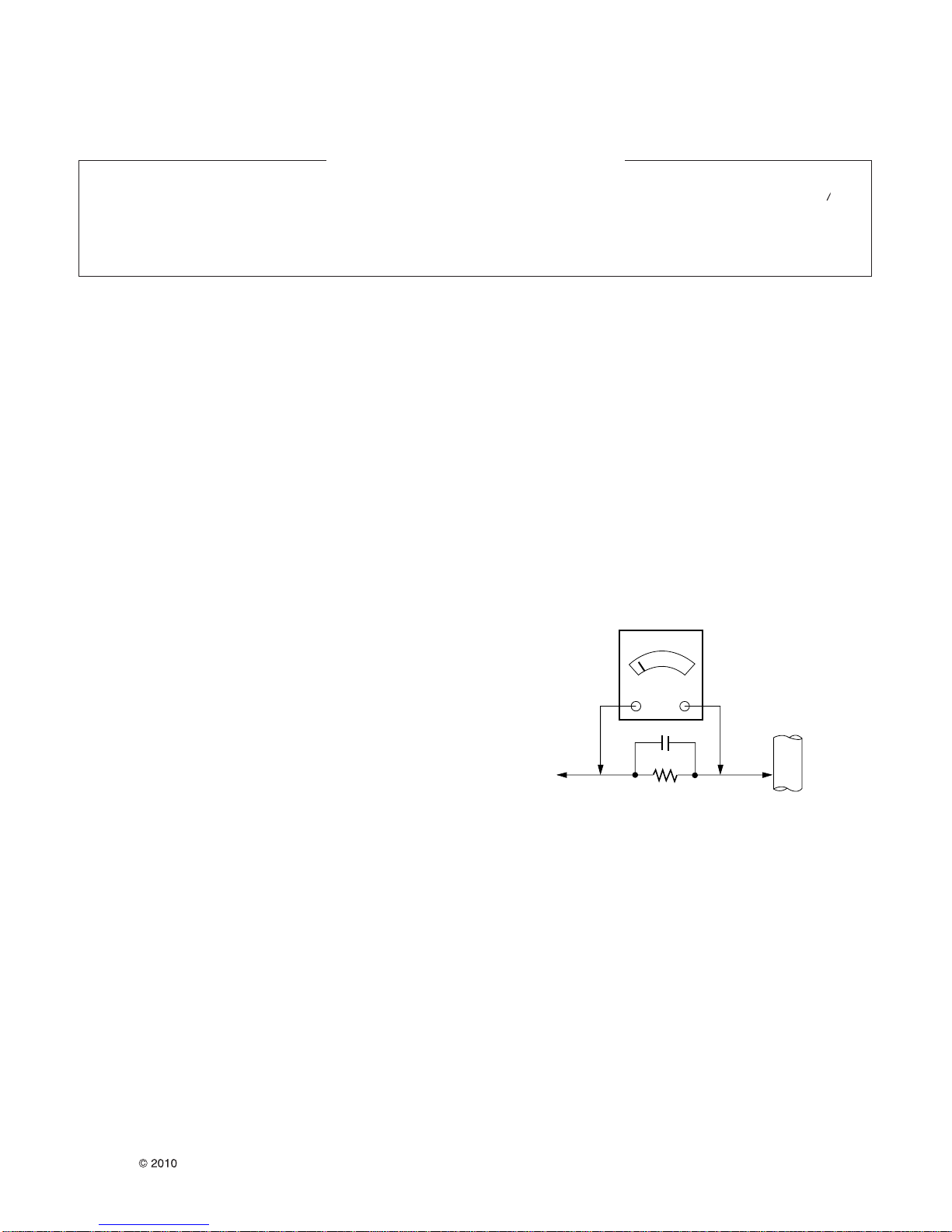
4.4. EDID D/L method
Recommend that don’t connect HDMI and RGB(D-SUB) cable
when downloading the EDID. If not possible, recommend that
connect the MSPG equipment.
There are two methods of downloading the edid data
4.4.1. 1st Method
EDID datas are automatically downloaded when adjusting the
Tool Options. Automatically downloaded when pushing the
enter key after adjusting the tool option5. It takes about
2seconds.
4.4.2. 2nd Method
Caution : Must be checked that the tool option is right or not.
If tool option is wrong, hdmi edid data could not be
downloaded well.
1) Press the ADJ key
2) Move to the 10. EDID D/L and Press the right direction
key(G)
3) Press the right direction key(G) at Start.
4) After about a few seconds, appear “Waiting..” => “OK”, then
compele.
4.4.3. RS-232C command Method
1) Command : AE 00 10
Caution : Don’t connect HDMI and RGB(D-SUB) cable when
downloading the EDID.
If the cables are connected, Downloading of edid
could be failed.
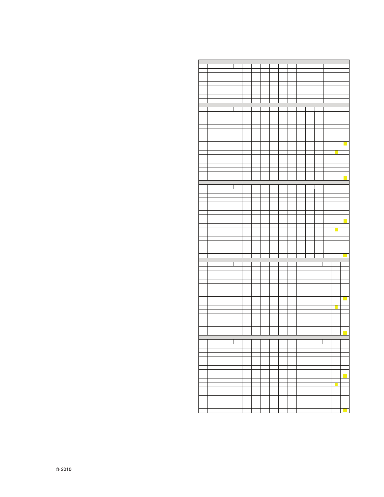
4.4.4. EDID data
4.4.4.1. LT03R M0DEL
** Analog(RGB): 128bytes
0 1 2 3 4 5 6 7 8 9 A B C D E F
0 00 FF FF FF FF FF FF 00 1E 6D 01 00 01 01 01 01
10 01 14 01 03 68 10 09 78 0A EE 91 A3 54 4C 99 26
20 0F 50 54 A1 08 00 81 80 61 40 45 40 31 40 01 01
30 01 01 01 01 01 01 02 3A 80 18 71 38 2D 40 58 2C
40 45 00 A0 5A 00 00 00 1E 01 1D 00 72 51 D0 1E 20
50 6E 28 55 00 A0 5A 00 00 00 1E 00 00 00 FD 00 3A
60 3E 1E 53 10 00 0A 20 20 20 20 20 20 00 00 00 FC
70 00 4C 47 20 54 56 0A 20 20 20 20 20 20 20 00 1D
**
HDMI 1 : 256Bytes
0 1 2 3 4 5 6 7 8 9 A B C D E F
0 00 FF FF FF FF FF FF 00 1E 6D 01 00 01 01 01 01
10 01 14 01 03 80 10 09 78 0A EE 91 A3 54 4C 99 26
20 0F 50 54 A1 08 00 71 4F 81 80 01 01 01 01 01 01
30 01 01 01 01 01 01 02 3A 80 18 71 38 2D 40 58 2C
40 45 00 A0 5A 00 00 00 1E 01 1D 00 72 51 D0 1E 20
50 6E 28 55 00 A0 5A 00 00 00 1E 00 00 00 FD 00 3A
60 3E 1E 53 10 00 0A 20 20 20 20 20 20 00 00 00 FC
70 00 4C 47 20 54 56 0A 20 20 20 20 20 20 20 01 D7
80 02 03 37 F1 4E 10 1F 84 13 05 14 03 02 12 20 21
90 22 15 01 26 15 07 50 09 57 07 78 03 0C 00 10 00
A0 B8 2D 20 C0 0E 01 40 0A 3C 08 10 18 10 98 10 58
B0 10 38 10 E3 05 03 01 01 1D 80 18 71 1C 16 20 58
C0 2C 25 00 A0 5A 00 00 00 9E 01 1D 00 80 51 D0 1A
D0 20 6E 88 55 00 A0 5A 00 00 00 1A 02 3A 80 18 71
E0 38 2D 40 58 2C 45 00 A0 5A 00 00 00 1E 00 00 00
F0 00 00 00 00 00 00 00 00 00 00 00 00 00 00 00 9B
** HDMI 2 : 256Bytes
0 1 2 3 4 5 6 7 8 9 A B C D E F
0 00 FF FF FF FF FF FF 00 1E 6D 01 00 01 01 01 01
10 01 14 01 03 80 10 09 78 0A EE 91 A3 54 4C 99 26
20 0F 50 54 A1 08 00 71 4F 81 80 01 01 01 01 01 01
30 01 01 01 01 01 01 02 3A 80 18 71 38 2D 40 58 2C
40 45 00 A0 5A 00 00 00 1E 01 1D 00 72 51 D0 1E 20
50 6E 28 55 00 A0 5A 00 00 00 1E 00 00 00 FD 00 3A
60 3E 1E 53 10 00 0A 20 20 20 20 20 20 00 00 00 FC
70 00 4C 47 20 54 56 0A 20 20 20 20 20 20 20 01 D7
80 02 03 37 F1 4E 10 1F 84 13 05 14 03 02 12 20 21
90 22 15 01 26 15 07 50 09 57 07 78 03 0C 00 20 00
A0 B8 2D 20 C0 0E 01 40 0A 3C 08 10 18 10 98 10 58
B0 10 38 10 E3 05 03 01 01 1D 80 18 71 1C 16 20 58
C0 2C 25 00 A0 5A 00 00 00 9E 01 1D 00 80 51 D0 1A
D0 20 6E 88 55 00 A0 5A 00 00 00 1A 02 3A 80 18 71
E0 38 2D 40 58 2C 45 00 A0 5A 00 00 00 1E 00 00 00
F0 00 00 00 00 00 00 00 00 00 00 00 00 00 00 00
AB
** HDMI 3 : 256Bytes
0 1 2 3 4 5 6 7 8 9 A B C D E F
0 00 FF FF FF FF FF FF 00 1E 6D 01 00 01 01 01 01
10 01 14 01 03 80 10 09 78 0A EE 91 A3 54 4C 99 26
20 0F 50 54 A1 08 00 71 4F 81 80 01 01 01 01 01 01
30 01 01 01 01 01 01 02 3A 80 18 71 38 2D 40 58 2C
40 45 00 A0 5A 00 00 00 1E 01 1D 00 72 51 D0 1E 20
50 6E 28 55 00 A0 5A 00 00 00 1E 00 00 00 FD 00 3A
60 3E 1E 53 10 00 0A 20 20 20 20 20 20 00 00 00 FC
70 00 4C 47 20 54 56 0A 20 20 20 20 20 20 20 01 D7
80 02 03 37 F1 4E 10 1F 84 13 05 14 03 02 12 20 21
90 22 15 01 26 15 07 50 09 57 07 78 03 0C 00 30 00
A0 B8 2D 20 C0 0E 01 40 0A 3C 08 10 18 10 98 10 58
B0 10 38 10 E3 05 03 01 01 1D 80 18 71 1C 16 20 58
C0 2C 25 00 A0 5A 00 00 00 9E 01 1D 00 80 51 D0 1A
D0 20 6E 88 55 00 A0 5A 00 00 00 1A 02 3A 80 18 71
E0 38 2D 40 58 2C 45 00 A0 5A 00 00 00 1E 00 00 00
F0 00 00 00 00 00 00 00 00 00 00 00 00 00 00 00 BB
** HDMI 4 : 256Bytes
0 1 2 3 4 5 6 7 8 9 A B C D E F
0 00 FF FF FF FF FF FF 00 1E 6D 01 00 01 01 01 01
10 01 14 01 03 80 10 09 78 0A EE 91 A3 54 4C 99 26
20 0F 50 54 A1 08 00 71 4F 81 80 01 01 01 01 01 01
30 01 01 01 01 01 01 02 3A 80 18 71 38 2D 40 58 2C
40 45 00 A0 5A 00 00 00 1E 01 1D 00 72 51 D0 1E 20
50 6E 28 55 00 A0 5A 00 00 00 1E 00 00 00 FD 00 3A
60 3E 1E 53 10 00 0A 20 20 20 20 20 20 00 00 00 FC
70 00 4C 47 20 54 56 0A 20 20 20 20 20 20 20 01 D7
80 02 03 37 F1 4E 10 1F 84 13 05 14 03 02 12 20 21
90 22 15 01 26 15 07 50 09 57 07 78 03 0C 00 40 00
A0 B8 2D 20 C0 0E 01 40 0A 3C 08 10 18 10 98 10 58
B0 10 38 10 E3 05 03 01 01 1D 80 18 71 1C 16 20 58
C0 2C 25 00 A0 5A 00 00 00 9E 01 1D 00 80 51 D0 1A
D0 20 6E 88 55 00 A0 5A 00 00 00 1A 02 3A 80 18 71
E0 38 2D 40 58 2C 45 00 A0 5A 00 00 00 1E 00 00 00
F0 00 00 00 00 00 00 00 00 00 00 00 00 00 00 00
CB