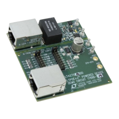
QUICK START GUIDE FOR DEMONSTRATION CIRCUIT 859
MULTIPLE OUTPUT PD
2
QUICK START PROCEDURE
Demonstration circuit 859 is easy to set up to evaluate
the performance of the LTC4267. For proper equipment
setup, refer to figure 1 and follow the procedure below:
1.
With the power source to the PSE turned off, con-
nect the input power supply to the board through the
J1 filtered Ethernet connector.
2.
In addition to a PSE, the DC859 board can be pow-
ered by an alternate input power supply through the
V+ (TP5) and VPORTN (TP14) terminals. Do not
connect more than one power source.
3.
Set the SIGNATURE jumper (JP1) to the ENABLE
position.
4.
Turn on the PSE or alternate input power supply and
increase the voltage until the power converter turns
on. Be careful not to exceed 57VDC. NOTE: Make
sure that the input voltage does not exceed 57VDC.
If a higher voltage is required, power components
with higher voltage ratings should be used.
5.
Verify proper classification and signature detection.
6.
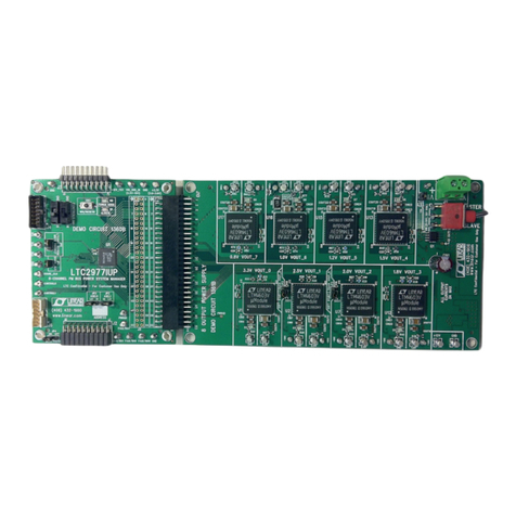
Check the output voltages. They should be as listed
in table 1. If there is no output, temporarily discon-
nect the load to make sure that the load is not set
too high.
7.
Once the proper output voltage is established, adjust
the load current within the appropriate range and
observe the output regulation, ripple voltage, effi-
ciency and other parameters.
OPERATION
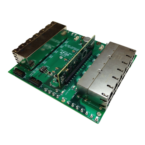
Demonstration circuit 859 interfaces with a customer’s
Power-Over-Ethernet test setup per Figure 1. The front
end of the demo circuit implements the required
Ethernet input interface transformer coupling and
common-mode termination through the integrated
connector J1. The demonstration circuit is set up to
allow data to pass in and back out of the demo circuit
while the DC859 performs IEEE 802.3af interface func-
tions. The Power Sourcing Equipment (PSE) is con-
nected to J1 and the PHY is optionally connected to
J2.
The PD is required to have 0.1uF of capacitance during
detection; this is provided by C2. It is also required to
have at least 5uF of capacitance after the in-rush cir-
cuit, provided by capacitors C1 and C9.
This demo circuit allows detection and power classifi-
cation of the PD per the IEEE 802.3af specification.
During the detection process of a PD, the LTC4267
displays the proper 25k
Ω
signature resistor. Signa-
ture detection may be disabled, if so desired, by set-
ting the SIGNATURE jumper (JP1) to the DISABLE po-
sition. If signature classification is disabled, all inter-
face functions of the LTC4267 are disabled. Signature
detection, classification and the internal power
MOSFET switch are all disabled.
Classification is programmed by the selection of a sin-
gle external resistor, RClass, connected to the RCLASS
pin on the LTC4267.
After detection and classification, the PD is powered
up when the input voltage exceeds the LTC4267 turn-
on under-voltage lock out (UVLO) through a dual-level
current-limited power switch. While the voltage be-
tween POUT and VPORTN is above the Power Good
trip point, the amperage through the power switch is
held below the low-level current limit. When the volt-
age between POUT and VPORTN falls below the Power
