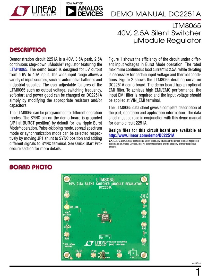
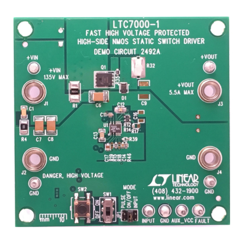
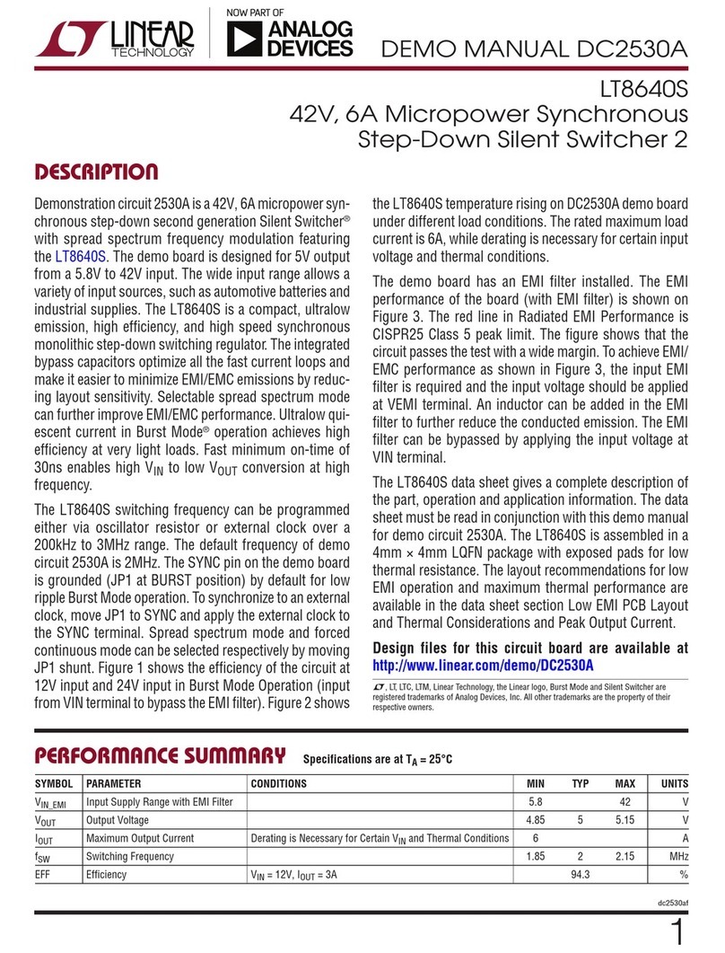
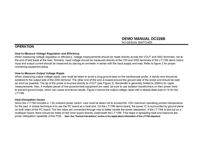
Linear Technology DC252 Quick setup guide

1
DEMO MANUAL DC252
DESIGN-READY SWITCHER
LTC1736 5-Bit VID Constant
Frequency Synchronous DC/DC Converter
, LTC and LT are registered trademarks of Linear Technology Corporation.
DESCRIPTIO
U
PERFOR A CE SU ARY
UW
WW
Burst Mode and OPTI-LOOP are trademarks of Linear Technology Corporation.
Demonstration Circuit DC252 is designed for mobile 5-bit
VID-programmed notebook CPU applications using the
LTC
®
1736 switching regulator controller. A high perfor-
mance, constant frequency current mode architecture
generates a precise low voltage CPU core supply. Protec-
tion features include an externally defeatable overcurrent
latchoff and internal current foldback for overload condi-
tions. A soft-latched crowbar monitors the output voltage
for overvoltage protection. OPTI-LOOP
TM
compensation
allows the transient response to be optimized over a wide
range of output capacitance and ESR values. The circuit
wasdesignedfora5Vto24Vinputrangebutallowsa4.5V
to 28V range (limited by the external MOSFETs). Strong
output drivers easily handle large power MOSFETs effi-
ciently. Output voltages can be configured according to
Intel mobile VID standards of 0.9V to 2.0V. An internal
power-goodcircuitmonitorstheoutputvoltageforout-of-
regulationconditions.Externalfrequencysynchronization
isprovided,asarethreemodesofoperation:BurstMode
TM
operation to reduce switching losses and maintain high
operating efficiencies, burst inhibit/forced continuous
mode and a low noise pulse-skipping mode that provides
constant frequency operation down to 1% maximum load
currents with low quiescent current. This results in a
power supply that has very high efficiency, low ripple and
fast transient response. Gerber files for this circuit board
are available. Call the LTC factory.
PARAMETER CONDITIONS VALUE
Input Voltage Range (Maximum Input Voltage Limited By External MOSFET and Input Capacitor) 5V to 24V
Output Output Voltage (Programmed with a 5-Bit Mobile VID Code) 0.9V to 2.0V
Max Output Current (Continuous) 11.0A
Max Output Current (Peak) 12A
Typical Output Ripple Measured with 10MHz Bandwidth (Burst Mode Operation) I
O
= 100mA 45mV
P-P
Typical Output Ripple Measured with 10MHz Bandwidth (Continuous) I
O
= 5A 20mV
P-P
V
IN
Line Regulation 5V to 24V 0.002%/V
LOAD CURRENT (A)
10mA 100mA 1A 10A
EFFICIENCY (%)
252 TA01
100
90
80
70
60
50
40
VIN = 5V
EXTVCC = 5V
VIN = 24V VIN = 15V
Efficiency
TYPICAL PERFOR A CE CHARACTERISTICS A D BOARD PHOTOS
UUW
Solder SideComponent Side

2
DEMO MANUAL DC252
DESIGN-READY SWITCHER
PERFOR A CE SU ARY
UW
WW
PARAMETER CONDITIONS VALUE
I
OUT
Load Regulation: No Load to Full Rated Output –0.3%
I
Q
Supply Current (Typical), No Load, V
IN
= 15V, FCB = INTV
CC
950µA
Supply Current in Shutdown (Typical), V
IN
= 15V 15µA
I
EXTVCC
EXTV
CC
Pin Current, V
EXTVCC
= 5V, V
IN
= 10V, FCB = INTV
CC,
No Load, V
OUT
= 1.6V 850µA
V
RUN
Run Pin Threshold (Typical) 1.3V
Frequency Operating Frequency (Typical), C
OSC
= 47pF 270kHz
1
2
3
4
5
6
7
8
9
10
11
12
TOP VIEW
G PACKAGE
24-LEAD PLASTIC SSOP
24
23
22
21
20
19
18
17
16
15
14
13
C
OSC
RUN/SS
I
TH
FCB
SGND
PGOOD
SENSE
–
SENSE
+
V
FB
V
OSENSE
VID0
VID1
TG
BOOST
SW
V
IN
INTV
CC
BG
PGND
EXTV
CC
VIDV
CC
VID4
VID3
VID2
LTC1736CG24
PACKAGE A D SCHE ATIC DIAGRA
WUW
1
2
3
4
5
6
7
8
9
10
11
12
24
23
22
21
20
19
18
17
16
15
14
13
COSC
RUN/SS
ITH
FCB
SGND
PGOOD
SENSE–
SENSE+
VFB
VOSENSE
VID0
VID1
TG
BOOST
SW
VIN
INTVCC
BG
PGND
EXTVCC
VIDVCC
VID4
VID3
VID2
LTC1736
U1
C1
47pF
RCS1
0.004ΩVOUT
0.9V TO 2V/11A
E7
VOSNS
E11
GND
E8
+CO1, CO2, C04, C06
180µF
4V
X4
247 F01
RS1
10Ω
L1
1.2µH
CB1
0.22µF
+
C2
4.7µF
M2
FDS6680A
M1, M3
FDS6680A
2X
D1
CMDSH-3
D2
MBRS340T3
C4
1µF
CS1
1000pF
R1
100k
EXTVCC
E2
PGOOD
E1
C3
47pF
RF1
4.7Ω
CF1
0.1µF
FCB/SYNC
E4
JP1
BURST MODE
JP2
LATCHOFF
RUN
E3
INTVCC
OFF
ON
+CIN3
22µF
30V
CIN1
22µF
30V
JP4
B0 B4
LSB MSB
JP3
PGOOD
INTVCC
R6
680k
+
CSS1
0.1µF
CC2
330pF RC1
33k
COSC1
47pF
CC1
47pF
R5, 10Ω
R2, 10Ω
R8
0Ω
+VIN
E10
GND
E9
Figure 1. Demo Board Schematic

3
DEMO MANUAL DC252
DESIGN-READY SWITCHER
PARTS LIST
REFERENCE QUANTITY PART NUMBER DESCRIPTION VENDOR TELEPHONE
C1, C3 2 08055A470JAT1A 47pF 50V 5% NPO Capacitor AVX (843) 946-0362
C2 1 TACR475M010R 4.7µF 10V 20% Tantalum Capacitor AVX (207) 282-5111
C4 1 0805ZC105MAT1A 1µF 10V 20% X7R Capacitor AVX (843) 946-0362
CC1 1 08055A470JAT1A 47pF 50V 5% NPO Capacitor AVX (843) 946-0362
CC2 1 08055A331MAT1A 330pF 50V 5% NPO Capacitor AVX (843) 946-0362
CB1 1 08055A224KAT1A 0.22µF 50V 20% X7R Capacitor AVX (843) 946-0362
CF1, CSS1 2 08055A104MAT1A 0.1µF 50V 20% X7R Capacitor AVX (843) 946-0362
CIN1, CIN3 2 30SC22M 22µF 30V OS-CON Capacitor SANYO (619) 661-6835
CIN1, CIN3 OPT THCR70E1H2262T 22µF 50V 20% Y5U Capacitor MARCON (847) 696-2000
CO1, CO2, CO4, CO6 4 EEFUE0G181R 180µF 4V SP Capacitor PANASONIC (201) 348-7522
CO1, CO2, CO4 OPT T510X447MOO6AS 470µF 6.3V Low ESR Tantalum Capacitor KEMET (408) 986-0424
CO3, CO5 OPT 4SP820M 820µF 4V OS-CON Capacitor SANYO (619) 661-6835
C
OSC1
1 08055A470JAT1A 47pF 50V 5% NPO Capacitor AVX (843) 946-0362
CS1 1 08055A102MAT1A 1000pF 50V 5% NPO Capacitor AVX (843) 946-0362
D1 1 CMDSH-3 BVR = 30V, 0.1A Schottky Diode CENTRAL (516) 435-1110
D2 1 MBRS340T3 BVR = 40V, 3A Schottky Diode ON SEMICONDUCTOR (800) 282-9855
E1, GND, +V
IN
, V
OSNS
, V
OUT1
5 1593-2 Turret Terminal (Small) KEYSTONE (718) 956-8900
E2, E3, E4, E8, E9, GND, 8 1502-2 Turret Terminal KEYSTONE (718) 956-8900
+V
IN
, +V
OUT
JP1 1 2802S-03-G2 2mm 3-Pin Header COMM CON (626) 301-4200
JP2, JP3 2 2802S-02-G2 2mm 2-Pin Header COMM CON (626) 301-4200
JP4 1 2202S-05-G2 2mm Dual 5-Pin Header COMM CON (626) 301-4200
L1 1 ETQP6F1R2HFA 1.2µH Inductor PANASONIC (201) 348-7522
M1, M2, M3 3 FDS6680A 30V 0.013ΩN-Channel MOSFET FAIRCHILD (408) 822-2126
R1 1 CR10-104JM 100k 1/10W 5% Chip Resistor TAD (800) 508-1521
R2, R5, RS1 3 CR10-100FM 10Ω1/10W, 1% Chip Resistor TAD (800) 508-1521
R6 1 CR10-685JM 680k 1/10W 5% Chip Resistor TAD (800) 508-1521
R8 1 CR10-0R0JM 0Ω1/10W Chip Resistor TAD (800) 508-1521
RC1 1 CR10-333JM 33k 1/10W 5% Chip Resistor TAD (800) 508-1521
RCS1 1 LRF2010-01-R004F 0.004Ω1/2W 1% Resistor IRC (361) 992-7900
RF1 1 CR10-470JM 4.7Ω1/10W, 5% Chip Resistor TAD (714) 255-9123
U1 1 LTC1736CG IC, LTC1736CG24 LTC (408) 432-1900
8 CCIJ2mm-138-G JUMPER COMM CON (626) 301-4200

4
DEMO MANUAL DC252
DESIGN-READY SWITCHER
This demonstration board is easy to set up to evaluate
the performance of the LTC1736. Please follow the
procedure outlined below for proper operation. Sol-
dered wire connections are required to properly evalu-
ate the performance of this switching regulator.
• RefertoFigure2forproperconnection ofmonitoring
and measurement equipment.
• Connect the input power supply to the V
IN
and GND
terminals on the right-hand side of the board with
soldered connections. Do not increase V
IN
over 28V
or the MOSFET(s) WILL BE DAMAGED.
• Connect the load between the V
OUT
and GND termi-
nals on the right side of the board with soldered
connections.
• The RUN pin can be left unconnected. To shut down
the LTC1736, tie this pin to ground.
• Set jumper JP4 for the desired output voltage. (See
Table 1.)
• If an external 5V supply is used, connect it to EXTV
CC
.
• Set the jumper JP1 so that FCB selects the desired
mode:
JP1 MODE
On Burst Mode Operation, Connect PGood to FCB/Sync
Off Forced Continuous
Open Apply External Clock to FCB/Sync
• Jumper JP2 determines if the overcurrent latchoff is
enabled. With JP2 installed this function is disabled.
Remove JP2 to enable.
JP2 OVERCURRENT LATCHOFF
Installed Disabled
Removed Enabled
• Active loads can cause confusing results. Refer to the
active load discussion in the Operation section.
QUICK START GUIDE
I TRODUCTIO
UU
The circuit in Figure 1 highlights the capabilities of the
LTC1736.
The LTC1736 is a synchronous step-down switching
regulator controller that drives external N-channel power
MOSFETs using a fixed frequency architecture with OPTI-
LOOPcompensation.OPTI-LOOPcompensationeffectively
removestheconstraintsplacedonC
OUT
byothercontrollers
for proper operation (such as restrictions on very low
ESRs). Burst Mode operation provides high efficiency at
low load currents. Operating efficiencies typically exceed
80% over more than two decades of load current range.
Do not use spring clip leads when testing this circuit.
Soldered wire connections are required to properly test
the performance of the PC board.
Thisdemonstrationcircuitis intendedfortheevaluationof
the LTC1736 switching regulator IC and was not designed
for any other purpose.
LTC1736CG
DEMO CIRCUIT DC252A
(408) 432-1900
VID CPU POWER CONVERTER
JP2 LATCHOFF
JP3
PGOOD VO
PROG
JP4
B4B0
JP1 BURST
EXT CLOCK
(REMOVE JP1 IF USED)
FCB/SYNC
EXTVCC
PGOOD
OFF
ON
GND
GND
GND
VOSNS
+VOUT
+VIN IIN
RUN
–
+LOAD
VOUT
IOUT
+
–
+
–
OPTIONAL REMOTE
VOUT SENSE CONNECTION
OPTIONAL EXTERNAL
HIGH FREQUENCY
SOURCE CONNECTION
A
A
252 F02
VIN
Figure 2

5
DEMO MANUAL DC252
DESIGN-READY SWITCHER
The operating frequency is set by an external capacitor,
C
OSC1
, allowing maximum flexibility in optimizing effi-
ciency. In this application, the frequency is set to 270kHz.
A multifunction control pin, FCB, inhibits Burst Mode
operation (reducing noise and RF interference), as well as
allowing synchronization to an external oscillator.
Soft-start is provided by an external capacitor, C
SS1
,
which can be used to properly sequence supplies. The
operating current level is user programmable via an exter-
nal current sense resistor and is set to 11A. Short-circuit
current is limited to approximately 4A by internal current
foldback.
Measuring Voltage Regulation
When trying to measure voltage regulation, remember
that all measurements must be taken at the point of
regulation. This point is where the LTC1736’s control loop
looks for the information to keep the output voltage
constant. In this demonstration board it is located be-
tween Pin 5 (SGND) of the LTC1736 and the sense side of
R
S1
. This point corresponds to the V
OSNS
terminal of the
board. Output voltage test leads should be attached di-
rectly to this terminal. The load should be placed across
the V
OUT
(E7) and GND (E8) terminals. Measurements
shouldnot
betakenattheendoftestleadsattheload;refer
to Figure 2 for the proper monitoring equipment configu-
ration.
This applies to line regulation (input to output voltage
regulation) as well as load regulation tests. In doing line
regulation tests, always look at the input voltage across
the input terminals.
Remote Output Voltage Sensing
Remote output voltage sensing can be accomplished by
connecting the V
OSNS
terminal with another wire directly
to the load. A 10Ωresistor, R
S1
, connects V
OUT
to V
OSNS
to avoid open sense conditions. Never under any circum-
stance connect the load to V
OSNS
!
Output Voltage Programming
Theoutput voltage is digitallysetto levels between 0.925V
and 2.00V using the voltage identification (VID) inputs B0
toB4set by jumper JP4. Theinternal5-bitDACconfigured
OPERATIO
U
as a precision resistor voltage divider sets the output
voltage in 50mV/25mV increments according to Table 1.
Table 1. VID Output Voltage Programming
B4 B3 B2 B1 B0 V
OUT
(V)
0 0 0 0 0 2.000V
0 0 0 0 1 1.950V
0 0 0 1 0 1.900V
0 0 0 1 1 1.850V
0 0 1 0 0 1.800V
0 0 1 0 1 1.750V
0 0 1 1 0 1.700V
0 0 1 1 1 1.650V
0 1 0 0 0 1.600V
0 1 0 0 1 1.550V
0 1 0 1 0 1.500V
0 1 0 1 1 1.450V
0 1 1 0 0 1.400V
0 1 1 0 1 1.350V
0 1 1 1 0 1.300V
01111 *
1 0 0 0 0 1.275V
1 0 0 0 1 1.250V
1 0 0 1 0 1.225V
1 0 0 1 1 1.200V
1 0 1 0 0 1.175V
1 0 1 0 1 1.150V
1 0 1 1 0 1.125V
1 0 1 1 1 1.100V
1 1 0 0 0 1.075V
1 1 0 0 1 1.050V
1 1 0 1 0 1.025V
1 1 0 1 1 1.000V
1 1 1 0 0 0.975V
1 1 1 0 1 0.950V
1 1 1 1 0 0.925V
11111 **
Note: *, ** Represents codes without a defined output voltage as
specified in Intel specifcations. The LTC1736 interprets these codes as a
valid input and produces output voltage as follows: [01111] = 1.250V,
[11111] = 0.900V.

6
DEMO MANUAL DC252
DESIGN-READY SWITCHER
The VID codes (00000-11110) are engineered to be com-
patible with Intel Mobile Pentium
®
II
Processor specifica-
tions for output voltages from 0.925V to 2.00V.
The LSB (B0) represents 50mV increments in the upper
voltage range (2.00V to 1.30V) and 25mV increments in
the lower voltage range (1.275V to 0.925V). The MSB is
B4. When all bits are low or grounded, the output voltage
is 2.00V.
Each VID digital input is internally pulled up by a 40k
resistor in series with a diode from VIDV
CC
. Therefore,
digital inputs must be grounded to get a digital low input,
and digital inputs can be either left unconnected or con-
nected to VIDV
CC
to get a digital high input. The series
diode is used to prevent the digital inputs from being
damagedorclampediftheyaredrivenhigherthanVIDV
CC
.
The digital inputs accept CMOS voltage levels.
Maximum Input Voltage Considerations
The recommended maximum input voltage of this board
is 24V for nominal output voltages. The minimum on-time
for the LTC1736 is generally about 200ns and the operat-
ingfrequencyforthisboard issetto270kHz.Thisimposes
a limit on the maximum input voltage when programming
low output voltages. For output voltages below 1.2V the
maximum input voltage is limited to:
V
IN(MAX)
< 20 (V
OUT
)
If a higher operating input voltage is required with V
OUT
<
1.2V, the operating frequency can be decreased by in-
creasing C
OSC1
. Refer to the LTC1736 data sheet for
details.If thedutycycle fallsbelowwhat canbeaccommo-
dated by the minimum on-time, the LTC1736 will begin to
skip cycles. The output voltage will continue to be regu-
lated, but the ripple current and ripple voltage will in-
crease.
Power-Good Output
A window comparator monitors the output voltage and its
open-drain output (E1) is pulled low when the divided
outputvoltageisnotwithin±7.5%ofthereferencevoltage
of 0.8V. Jumper JP3 connects pull-up resistor R1 from
INTV
CC
to the power-good output, E1. This jumper is
provided to allow other pull-up voltages to be used. Make
OPERATIO
U
sure the maximum voltage on PGOOD is less than 7V.
During shutdown, the PGOOD output is pulled low.
INTV
CC
Regulator
An internal, P-channel, low dropout regulator produces
the 5.2V supply that powers the drivers and internal
circuitry within the LTC1736. The INTV
CC
pin can supply
up to 50mA (this includes the gate-drive currents). Exter-
nal loading of the INTV
CC
pin can be thermally limited
(allow 10mA to 20mA for gate-drive currents). At high
input voltages, the maximum junction temperature rating
for the LTC1736 may be exceeded if too large an external
load is placed on INTV
CC
. See the LTC1736 data sheet for
details.
EXTV
CC
Connection
The LTC1736 contains an internal P-channel MOSFET
switch connected between the EXTV
CC
and INTV
CC
pins.
The switch closes and supplies the INTV
CC
power when-
ever the EXTV
CC
pin is above 4.7V; it remains closed until
EXTV
CC
drops below 4.5V. This allows the MOSFET driver
and control power to be derived from the EXTV
CC
pin
instead of V
IN
. Do not apply greater than 7V to the EXTV
CC
pin and ensure that EXTV
CC
< V
IN
. Additional efficiency
gains can be realized by powering INTV
CC
from other high
efficiency sources, such as a 5V system power supply.
The following list describes the most common possible
connections for EXTV
CC
for low output voltage applica-
tions:
1. EXTV
CC
left open (or grounded); this will cause INTV
CC
to be powered from the internal 5.2V regulator resulting in
an efficiency penalty at low load currents and high input
voltages.
2. EXTV
CC
connected to an external supply ; if an external,
high efficiency supply is available in the 5V to 7V range
(EXTV
CC
<V
IN
),itmaybeusedtopowerEXTV
CC
,providing
an efficiency boost. The typical connection in a notebook
CPU power solution is to connect it to the main 5V system
power supply.
Pentium is registered trademark of Intel Corportion.

7
DEMO MANUAL DC252
DESIGN-READY SWITCHER
OPERATIO
U
Low Current Modes and Synchronization
The FCB input pin, set by jumper JP1 and FCB/Sync
terminal E4, allows the selection of the low current oper-
ating mode and external frequency synchronization of the
switching regulator.
Tying the FCB pin to ground with JP1 forces the controller
into PWM or forced continuous mode. In forced continu-
ousmode,theoutput MOSFETsarealwaysdriven,regard-
less of output loading conditions. Operating in this mode
allows the switching regulator to source or sink current—
butbe careful; when the outputstage sinks current, power
is transferred back into the input supply terminals and the
input voltage rises.
Burst Mode operation is enabled when the voltage applied
tothe FCBpinisgreater than0.8V(i.e., JP1 tiedtoINTV
CC
)
orifthepinisleftopen.Acomparatorwithaprecision0.8V
thresholdallowsthepin tobeusedtoregulateasecondary
winding on the switching regulator’s output. A small
amount of hysteresis is included in the design of the
comparator to facilitate clean secondary operation. When
the resistively divided secondary output voltage falls be-
low the 0.8V threshold, the controller operates in the
forced continuous operating mode for as long as it takes
tobring the secondary voltageabovethe0.8V + hysteresis
level.
The internal LTC1736 oscillator can be synchronized to an
external oscillator by clocking the FCB pin with a signal
above 1.5V
P-P
(Remember to remove jumper JP1). When
the LTC1736 is synchronized to an external frequency,
Burst Mode operation operation is disabled but cycle
skipping is allowed at low load currents, since current
reversal is inhibited. The bottom gate will come on every
10 clock cycles to ensure that the bootstrap capacitor C
B1
is kept charged. The rising edge of an external clock
applied to the FCB pin starts a new cycle.
When the LTC1736 is synchronized to an external clock,
burst inhibit mode allows heavily discontinuous, low
audio noise, constant frequency operation down to ap-
proximately 1% of maximum designed load current. This
mode results in the elimination of switching frequency
subharmonics over 99% of the output load range. Switch-
ing cycles start to be dropped at approximately 1% of
maximum designed load current in order to maintain
proper output voltage.
The range of synchronization is from 240kHz to 350kHz
with C
OSC
= 47pF. Attempting to synchronize to a higher
frequency than 350kHz can result in inadequate slope
compensation and cause loop instability with high duty
cycles. If loop instability is observed while synchronized,
additional slope compensation can be obtained by simply
decreasing C
OSC
.
The following table summarizes the possible states avail-
able on the FCB/Sync pin:
FCB/SYNC PIN CONDITION
DC Voltage: 0V to 0.7V Burst Disabled/Forced Continuous
Current Reversal Enabled
DC Voltage: ≥0.9V Burst Mode Operation,
No Current Reversal
Feedback Resistors Regulating a Secondary Winding
Ext Clock: (0V to V
FCB/SYNC
) Burst Mode Operation Disabled
(V
FCB/SYNC
> 1.5V) No Current Reversal
DC252 Modifications (MOSFETs)
The DC252 demo board has various modification provi-
sions. Additional pad locations are available for adding
extraoutput capacitors together with an extra footprint for
a parallel topside MOSFET.
When operating at high input voltages, the transition
losses of the topside MOSFET (M2) become very signifi-
cant. Be sure to consider power loss due to transition
losses as well as R
DS(ON)
losses. Don’t over specify the
topside MOSFET. (Refer to the LTC1736 data sheet for
details.)
RefertotheLTC1736 data sheet for further information on
the internal operation and functionality descriptions of the
IC.
DC252 Modifications (Output Capacitors)
Four Matsushita SP output capacitors are installed on the
demoboard.Otheroutputcapacitors mayfreelybesubsti-
tuted provided they meet the load transient requirements.
OPTI-LOOP compensation allows the transient response
to be optiumized over a wide range of output capacitance
and ESR values while minimizing output capacitance.

8
DEMO MANUAL DC252
DESIGN-READY SWITCHER
The output capacitors are generally determined by ESR
(effective series resistance) and voltage rating rather than
capacitance. The ESR must be small enough that output
ripple voltage and any voltage droop due to high load
current transients stay within the specifications of the
CPU.Theoutputcapacitancemustbelargeenoughtohold
uptheoutputvoltageuntiltheinductorcurrenthasramped
up or down to its new value. With proper OPTI-LOOP
compensation components, the response time is opti-
mized and the output capacitance is minimized. The com-
pensation components installed on the demo board are
appropriatefor the output capacitors specified in theparts
list.
AdditionalmountinglocationsexistforthroughholeSanyo
OS-CON output capacitors, should they be desired. Com-
binations of different types of capacitors have proved to
yield cost effective solutions. ESL (equivalent series in-
ductance), typically not specified, can reduce the effec-
tiveness of the ESR at high load current slew rates, so be
careful in specifying the output capacitor.
Overcurrent Protection
TheRUN/SScapacitor, C
SS1
,
isusedinitially toturnonand
limit the inrush current of the controller. After the control-
ler has been started and given adequate time to charge the
outputcapacitorandprovidefullloadcurrent,C
SS1
isused
asashort-circuittime-outcircuit.Iftheoutputvoltagefalls
to less than 70% of its nominal value, C
SS1
begins dis-
charging on the assumption that the output is in an
overcurrentand/orshort-circuit condition.Ifthecondition
lasts for a long enough period, as determined by the size
of C
SS1
, the controller will be shut down until the RUN/SS
pin voltage is recycled. This built-in latchoff can be over-
ridden by providing >5µA pull-up at a compliance of 4V to
the RUN/SS pin by installing jumper JP2. This current
shortens the soft-start period but also prevents net dis-
charge of the RUN/SS capacitor during an overcurrent
and/or short-circuit condition.
Foldback current limiting is activated when the output
voltagefallsbelow70%ofitsnominallevel,whetherornot
the short-circuit latchoff circuit is enabled.
With the overcurrent latchoff enabled, a slow ramp on the
input voltage may cause the circuit to latch off. Simply re-
cycle the run pin to start. Refer to the LTC1736 data sheet
for details.
Overvoltage Protection
Theoutput isprotectedfrom overvoltage bya“soft-latch.”
When the output voltage exceeds the regulation value by
more than 7.5%, the synchronous MOSFET turns on, and
remains on for as long as the overvoltage condition is
present.Iftheoutputvoltagereturnstoasafelevel,normal
operation resumes. This self-resetting action prevents
"nuisance trips" due to momentary transients and elimi-
nates the need for the Schottky diode that is necessary
with conventional OVP to prevent V
OUT
reversal.
Because of the inherent self-resetting action of the soft-
latch, dynamic changing of the VID control bits does not
latchofftheLTC1736.Whenanewoutputvoltageissetvia
the VID bits, the control loop simply adjusts the output
voltage and the overvoltage protection threshold to this
new level without causing a fault.
The overvoltage threshold tracks the new output voltage,
protecting the load at all times. Figure 3a and Figure 3b
both show an example of a dynamic VID code change
resulting in a programmed output voltage change from
1.5V to 1.3V at a constant 5 ampere load current. At the
instantthe VID code is changed, the control loop beginsto
respond to the new output voltage, and the power-good
output is asserted low since the new programmed output
voltage is outside the 7.5% window. When the new output
voltage is within 7.5% of its new programmed value, the
power-good signal goes high. Figure 3a shows a VID code
change with the FCB pin low (Burst Mode operation
disabled). Figure 3b shows a dynamic VID code change
with Burst Mode operation active. If dynamic VID changes
arerequiredandBurstModeoperationisdesired,connect
the PGOOD output (E1) to the FCB/Sync input (E4) and
remove jumper JP1. This connection automatically forces
continuous operation whenever the power-good output is
low, providing fast response to VID changes regardless of
load current.
Active Loads— Beware
Beware of active loads! They are convenient but problem-
atic. Some active loads do not turn on until the applied
OPERATIO
U
9
DEMO MANUAL DC252
DESIGN-READY SWITCHER
voltage rises above 0.1V to 0.8V. The turn-on may be
delayed as well. A switching regulator with soft-start may
appear to start up, then shut down and, eventually, reach
the correct output voltage. What happens is as follows: at
switching regulator turn-on, the output voltage is below
the active load’s turn-on requirements. The switching
regulator’s output rises to the correct output voltage level
due to the inherent delay in the active load. The active load
turns on after its internal delay and then pulls down the
switching regulator’s output because the switcher is in its
soft-start interval. The switching regulator’s output may
comeupatsome latertimewhenthesoft-startintervalhas
passed.
A switching regulator with foldback current limit will also
have difficulty with the unrealistic I-V characteristic of the
active load. Foldback current limiting will reduce the
outputcurrent available as the output voltage drops below
a threshold level (this level is 70% of nominal V
OUT
for the
LTC1736). This reduction in available output current will
result in the active load immediately pulling down the
output because the active load’s current demand remains
constant as the output voltage decreases. Most actual
loadsdonot behave liketheactiveload I-V characteristics.
Actual loads normally have a V
IN
• C • f dependency, where
C is internal chip capacitance and f is the frequency of
operation. To alleviate the active-load problem during
testing, the active load should be initially programmed to
a much lower current value until the switching regulator’s
soft-start interval has passed and then increased to the
higher level. The switching regulator will supply the in-
creased current required according to the transient re-
sponse of the switching regulator. Output capacitance
needs to be sufficient to accommodate the current step
during the transient period, keeping the output voltage at
or above the foldback threshold of 70%.
Checking Transient Response
OPTI-LOOP compensation effectively removes the con-
straints placed on C
OUT
by other controllers (such as
restrictions on very low ESRs). The output capacitors
used in this demo board have very low ESRs; other types
maybesubstitutedbutbecarefulltomeasuretheloadstep
transient response and verify the specfications on output
voltage continue to be met during transients.
A partial list of low ESR capacitors that are suitable for this
application is included in the parts list. Each has its own
cost, size, ESL and other performance trade offs. Combi-
nations of capacitors have been shown to work well, too,
so feel free to experiment. An example of a combination
that works well is an OS-CON, 820µF/4V capacitor in
parallel with a 180µF/4V Matsushita SP series capacitor.
The SP capacitor tames the ESL-induced characteristic of
OPERATIO
U
Figure 3a. Dynamic VID Change, Burst Mode Operation Defeated Figure 3b. Dynamic VID Change, Burst Mode Operation Enabled
252 F03a
PGOOD
5V/DIV
V
OUT
100mV/
DIV
I
L
5A/DIV
252 F03b
PGOOD
5V/DIV
VOUT
100mV/
DIV
IL
5A/DIV

10
DEMO MANUAL DC252
DESIGN-READY SWITCHER
the otherwise low ESR OS-CON. The I
TH
OPTI-LOOP
compensationcomponentsshown inFigure1’scircuitwill
provide an adequate starting point for most applications.
Theload-stepresponsewiththe output voltage set to 1.6V
is shown in Figures 4a and 4b using four 180µF/4V
Matsushita SP series for the output capacitors. Figure␣ 4a
is a 0A to 12A load step with Burst Mode operation
inhibited (FCB = 0V). Figure 4b shows the load step
response for a 10mA to 12A load current transition with
Burst Mode operation enabled (FCB = 5V).
The regulator loop response can be checked by looking at
the load current transient response. Switching regulators
take several cycles to respond to a step in DC (resistive)
load current. When a load step occurs, V
OUT
shifts by an
amount equal to ∆I
LOAD
(ESR), where ESR is the effective
series resistance of C
OUT
. ∆I
LOAD
also begins to charge or
discharge C
OUT
, generating the feedback error signal that
forces the regulator to adapt to the current change and
return V
OUT
to its steady-state value. During this recovery
time, V
OUT
can be monitored for excessive overshoot or
ringing, which would indicate a stability problem. OPTI-
OPERATIO
U
LOOP compensation allows the transient response to be
optimized over a wide range of output capacitances and
ESR values. The availability of the I
TH
pin not only allows
optimization of control loop behavior but also provides a
DC coupled and AC filtered closed-loop-response test
point. The DC step, rise time and settling at this test point
truly reflect the closed-loop response. Assuming a pre-
dominantlyfirstordersystem,phasemarginand/ordamp-
ing factor can be estimated using the percentage of
overshoot seen at this pin. The bandwidth can also be
estimated by examining the rise time at the pin.
The I
TH
series R
C1
–C
C2,
C
C1
filter sets the dominant pole-
zero loop compensation. The values can be modified
slightly (from 0.5 to 2 times their suggested values) to
optimize transient response once the final PC layout is
done and the particular output capacitor type and value
have been determined. The output capacitors need to be
decided upon because the various types and values deter-
mine the loop feedback factor gain and phase. An output
current pulse of 20% to 100% of full load current having
a rise time of 1µs to 10µs will produce output voltage and
Figure 4b. Load Step Response with
Burst Mode Operation Enabled
Figure 4a. Load Step Response with
Burst Mode Operation Disabled
V
OUT
50mV/DIV
I
L
5A/DIV
252 F04a
252 F04b
V
OUT
50mV/DIV
I
L
5A/DIV

11
DEMO MANUAL DC252
DESIGN-READY SWITCHER
PCB LAYOUT A D FIL
UW
Component Side Silkscreen Component Side Copper (Layer 1)
Internal Copper (Layer 2) Internal Copper (Layer 3)
OPERATIO
U
I
TH
pin waveforms that will give a sense of the overall loop
stability without breaking the feedback loop. The AC gain
of the loop will be increased by increasing R
C1
and the
bandwidthoftheloopwillbeincreasedbydecreasingC
C2
.
If R
C1
is increased by the same factor that C
C2
is de-
creased, the zero frequency will be kept the same, thereby
keeping the phase the same in the most critical frequency
range of the feedback loop. The output voltage settling
behavior is related to the stability of the closed-loop
system and will demonstrate the actual overall supply
performance.CapacitorC
C2
providessomehighfrequency
decouplingagainsttransients.Becarefullnottooverspecify
its value, as the response time to a load step will be
degraded.Again,monitoringtheI
TH
pinwillshowanyslew
rate limitations due to C
C1
. For further explanation of
optimizing loop response, refer to Application Note 76.
Information furnished by Linear Technology Corporation is believed to be accurate and reliable.
However, no responsibility is assumed for its use. Linear Technology Corporation makes no represen-
tationthat theinterconnectionofitscircuitsasdescribed hereinwillnotinfringeon existingpatent rights.

12
DEMO MANUAL DC252
DESIGN-READY SWITCHER
LinearTechnology Corporation
1630 McCarthy Blvd., Milpitas, CA 95035-7417
(408)432-1900
●
FAX:(408)434-0507
●
www.linear-tech.com
LINEAR TECHNOLOGY CORPORATION 1999
dc252f LT/TP 1199 500 • PRINTED IN USA
PCB LAYOUT A D FIL
UW
Bottom Side Paste Mask Component Paste Mask
PC FAB DRAWI G
U
Bottom Side SilkscreenBottom Side Copper (Layer 4)
NUMBER
SYMBOL DIAMETER OF HOLES PLATED
A 0.100 8 YES
B 0.070 2 NO
C 0.065 5 YES
D 0.045 18 YES
E 0.035 25 YES
F 0.025 2 YES
G 0.020 15 YES
A
A
A
A
B
B
C
C
C
D
D
D
D
D
D
E
E
G
G
GGG
G
GG
GG
GG
G
GG
E
E
E
E
E
E
E
E
EE
10 PLCS
EEE
E
E
E
E
EDDDDD
DDD
F
F
D
DDD
C
C
A
A
A
A
2.75"
2.10"
NOTES: UNLESS OTHERWISE SPECIFIED
1. ALL DIMENSIONS ARE IN INCHES, ±0.003. FINISHED HOLE SIZES ARE +0.003/–0.
2. FINISHED MATERIAL IS FR4, 0.062 THICK, 1 OZ Cu, 4 LAYERS.
PLATED HOLE WALL THICKNESS 0.001 MIN. INTERNAL LAYERS 1 OZ Cu.
3. PROCESS AND PLATING: SMOBC
4. SOLDERMASK BOTH SIDES USING GLOSSY GREEN LPI.
5. SILKSCREEN WHITE NONCONDUCTIVE INK BOTH SIDES.
252 PC Fab Dwg
Table of contents
Other Linear Technology Switch manuals

Linear Technology
Linear Technology LTC7000-1 Quick setup guide

Linear Technology
Linear Technology DC239 Quick setup guide

Linear Technology
Linear Technology LT8614 Quick setup guide

Linear Technology
Linear Technology DC2251A Quick setup guide

Linear Technology
Linear Technology DC2019A Quick setup guide

Linear Technology
Linear Technology DC2530A Quick setup guide

Linear Technology
Linear Technology DC326B Quick setup guide

Linear Technology
Linear Technology LTC4160EPDC User manual