1
dc1986af
DEMO MANUAL DC1986A
DESCRIPTION
LTM2892-I
I2C µModule Isolator
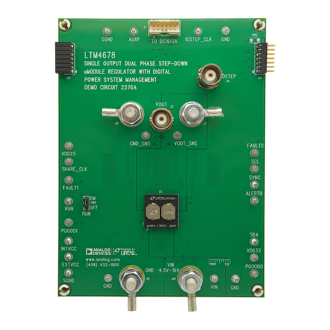
Demonstration circuit 1986A is an I2C µModule
®
Isolator
featuring the LTM2892-I. The demo circuit operates from
external supply voltages on VCC1, VL1, VCC2, and VL2. It
communicates all necessary signaling across the isolation
barrier through LTC’s Isolator™ µModule Technology.
L, LT, LTC, LTM, Linear Technology, the Linear logo and µModule are registered trademarks
and Isolator is a trademark of Linear Technology Corporation. All other trademarks are the
property of their respective owners.
PERFORMANCE SUMMARY
OPERATING PRINCIPLES
Design files for this circuit board are available at
http://www.linear.com/demo
Specifications are at TA= 25°C
SYMBOL PARAMETER CONDITIONS MIN TYP MAX UNITS
VCC1, VCC2 Input Supply Range 3.0 5.5 V
VL1, VL2 Logic Supply Range 3.0 5.5 V
fMAX Maximum Data Rate INx →OUTx, CL= 15pF 20 MHz
I2C Communication 400 kHz
VIORM Maximum Working Insulation Voltage GND1 to GND2 850 VDC
600 VRMS
Common Mode Transient Immunity 50 kV/µs
The LTM2892-I requires two to four external power sup-
plies for operation, one for power and one for the signal
interface, on each side of the isolation barrier. The logic
supplies may be tied to the input supplies. Isolation is
maintained by the separation of GND1 and GND2 where
significant operating voltages and transients can exist
without affecting the operation of the LTM2892-I. The ON1
and/or ON2 pins enable or shut down the LTM2892-I, both
must be driven to their respective logic supply voltage for
proper operation. All I2C or digital signals are referenced
to the logic supply pins VL1 or VL2.
I2C signaling does not require any additional components.
The demo board includes pull-up resistors on SDA1 and
SCLIN. SCLOUT and SDA2 donot require external pull-ups,
SCLOUT is a push-pull output and SDA2 is pulled high
through an integral current source within the LTM2892-I.
Do not use external pull-up resistors or current sources
on SCLOUT or SDA2.
I2C signaling is configured by defining the LTM2892-I
pins as follows:
Logic Side: SCLIN = SCL(IN), and SDA1 = SDA(IN).
IsolatedSide: SCLOUT= SCL(OUT),SDA2 =SDA(OUT).
Reference Figure 1 for schematic representation.
No special precautions are required for low RF emissions.
EMI performance is shown in Figure 2, measured using
a gigahertz transverse electromagnetic (GTEM) cell and
method detailed in IEC 61000-4-20, Testing and Measure-
ment Techniques – Emission and Immunity Testing in
Transverse Electromagnetic Waveguides.
