QUICK START GUIDE FOR DEMONSTRATION CIRCUIT 768
15A POLYPHASE MONOLITHIC SYNCHRONOUS BUCK REGULATOR
1
LTC3415
DESCRIPTION
D
emonstration Circuit
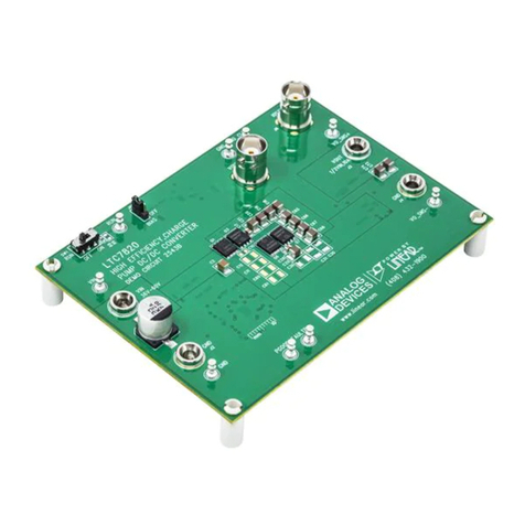
768 is a 15A high efficiency,
phase lockable constant frequency buck converter, in-
corporating two LTC3415 polyphase monolithic syn-
chronous regulators. The DC768 has an input voltage
range of 2.5V to 5.5V and an output voltage range from
0.6V to 5V. The reference voltage of 0.6V is +/-1% accu-
rate, producing a more precise output voltage. The op-
erating frequency range of the DC768 is either set by the
LTC3415 internal oscillator to 1.5 MHz, set to 1 MHz or 2
MHz by forcing the PLLPF pin to ground or Vin, respec-
tively, or synchronized to an external clock, with a range
between 750 kHz and 2.25 MHz. The DC768 can deliver
high power for monolithic parts – up to 15A of output
current – due to the high current power switches (28
m
Ω
of on-state resistance) of the LTC3415. The
LTC3415 also incorporates OPTI-LOOP compensation,
so that the DC768 can be optimized with external com-
ponents to provide fast transient response over a wide
range of line and load conditions. However, the
LTC3415 has internal compensation for those requiring a
simple high power supply only. The DC768 has two
LTC3415s operating in polyphase operation. Due to the
LTC3415 polyphase capability, multiple DC768s can be
paralleled for higher current power supplies. Since the
parallel LTC3415s operate out-of-phase, the amount of
input and output capacitance required will be minimal.
The DC768 offers the three standard modes of opera-
tion: force continuous, pulse-skipping, and Burst-
Mode
TM
, for those circuits that operate during intervals of
low output power. Extra features include tracking, for
easy power supply sequencing, output margining, power
good, and spread spectrum operation, which signifi-
cantly reduces the peak switching noise emitted from
the DC768. All these features make the DC768 perfectly
suited for high current, high power applications, such as
notebook or desktop computers.
Design files for this circuit board are available. Call
the LTC factory.
TM
- Burst Mode is a trademark of Linear Technology Corporation
Table 1.
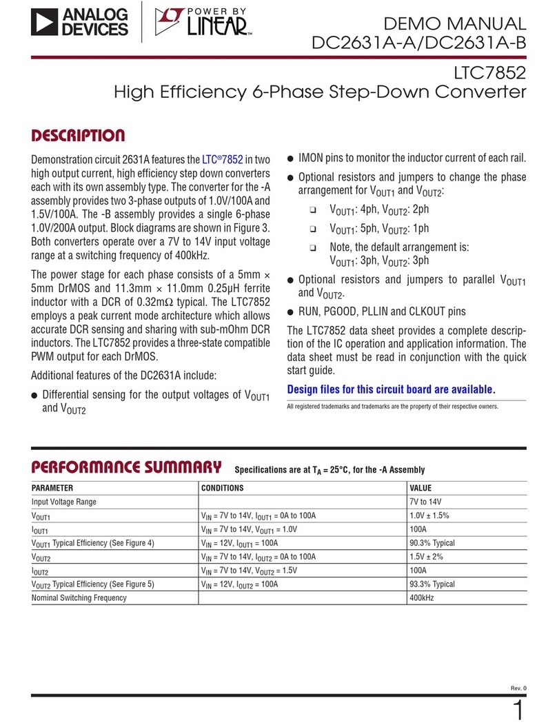
Performance Summary (TA= 25°C)
PARAMETER CONDITIONS VALUE
Minimum Input Voltage 2.5V
Maximum Input Voltage 5.5V
Output Voltage VOUT Regulation VIN = 2.5V to 5.5V, IOUT = 0A to 15A
1.2V ±3% (1.164V to 1.236V)
1.5V ±3% (1.455V to 1.545V)
1.8V ±3% (1.746V to 1.854V)
Typical Output Ripple VOUT VIN = 5V, IOUT = 15A (20 MHz BW) <20mVP–P
Burst Mode - VIN = 3.3V, VOUT = 1.8V <1.5A ±0.1A
Pulse-Skipping - VIN = 3.3V, VOUT = 1.8V < 5A ±0.1A
Operation Modes
Forced Continuous Any Output Current
Nominal Switching Frequency 1.5 MHz
