Lithium Grim PhotoFet Instruction Manual

PhotoFet
True Bypass Relay
Building Instructions
v1.0.1

PhotoFet True Bypass Relay v1.0.1
2
Table of contents
PCB layout ............................................................................................................................................... 3
Top-side............................................................................................................................................... 3
Bottom-side........................................................................................................................................ 3
Components ............................................................................................................................................ 4
The technique behind the switch............................................................................................................ 4
Build sequence ........................................................................................................................................ 5
Connecting the switch......................................................................................................................... 7
Optional SW2....................................................................................................................................... 7
Lining up the LED................................................................................................................................. 8
The finished switch............................................................................................................................ 10
Residual noise (LED popping) ............................................................................................................ 10
Off board wiring .................................................................................................................................... 11
Modes: Using the switch....................................................................................................................... 12
Troubleshooting .................................................................................................................................... 12
Schematic .............................................................................................................................................. 13
Read this entire manual thoroughly before you start building the effect! There are some available
options and you should choose which one you want to incorporate before starting your build.
Last update: 26-02-2021

PhotoFet True Bypass Relay v1.0.1
3
PCB layout
Top-side
Bottom-side
Dimensions: 24,6 mm x 34,7 mm
0.97 inch x 1.37 inch

PhotoFet True Bypass Relay v1.0.1
4
Components
All parts must be rated 25V+ if used in conjunction with a charge pump
Name
Value
Comment
C1
100u
Electrolytic
C2
100n
MKT, Wima or SMF
C3
100n
Ceramic
D1
1n5817
D2
1N4148
D3
LED
Color and type of personal choice
IC1
PIC12F675
OC1
TLP222A
R1
4k7
Led resistor
R2
1k5
REL1
NA5W-K
DPDT relay 5V alternative Omron G6S-2-5VDC
SW1
SPDT
Effect on - off (Momentary)
SW2
SPST
Momentary/Latching mode selection
VR1
LM78L05
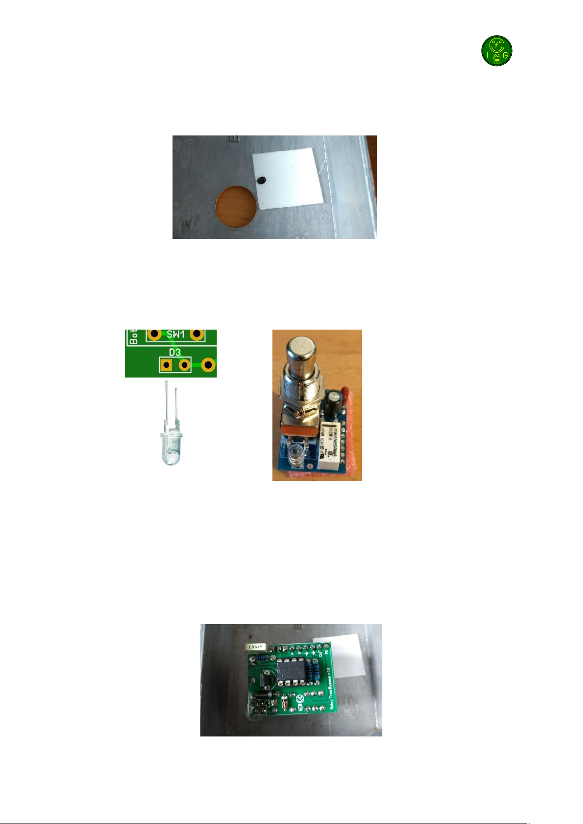
Make sure you also get some not to thick double sided tape
The technique behind the switch
Let’s start by emphasizing that the switch is guaranteed 100% true bypass and does not affect your
signal. The digital part is only used to switch the relay and light up the LED. The signal of your guitar
only goes through the DPDT part of the relay, which is electrically completely separate from the rest
of the switch.
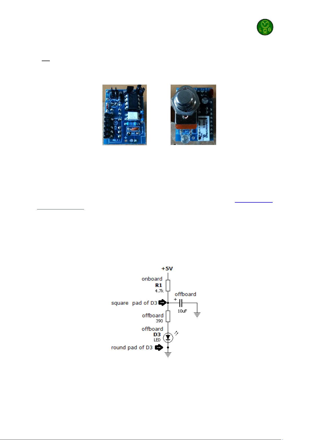
It works as follows. When you press the momentary switch (SW1) you are sending a signal to the
microcontroller which is picked up by the internal program. Depending on the state, it will in turn
either put +5V on the relay or remove the +5V from the relay. This way the switch will turn on and off
switching the DPDT relay. The state of the switch is saved to memory so when you disconnect it and
then reconnect it again, it will return in its last known state.
To prevent the switch from loud “popping”, the photocoupler comes in to play. It is turned on just
before the relay switches and grounds the output of the effect, making it totally silent. The relay
switches, the LED is turned on and then the photocoupler is released, thus removing ground from the
output and letting your signal flow through freely again. And all this in less than 60ms. The
photocoupler is not in the signal chain when you play and so does not affect your signal chain!
SW2 enables you to make the switch, which is by default latching (like all common effect switches),
act as a momentary switch. Depending on the state the switch was in before shorting SW2, it will
make the switch act as a “make”or “break”version. This way you can shortly activate an effect or
deactivate an effect while you stand on the switch. If you do not want this option, then the only thing
you have to do is not connect SW2. Simple! This feature is especially fun to make an effect act like a
kill switch. Lastly, the switch supports Longpress momentary mode. Read the “Using the switch”
chapter for all features.

PhotoFet True Bypass Relay v1.0.1
5
Build sequence
Soldering this board can be complicated for some people since the solder pads are very close
together and components must be placed on both sides of the board. Use a magnifying glass to make
the job easier. The trick to soldering a PCB is to work from small to big components. My building
sequence suggestions in this section are based on the parts I used myself. Sometimes some
components are smaller (or bigger) so always use your own common sense and change the order
accordingly. Usually capacitors differ a lot in size depending on their rating.
Note: Do not blow on your solder in an attempt to cool it down. That will possibly result in a bad join
that might corrode! Watch this video from EEVblog (no that’s not me) to learn more.
This PCB is made to fit the relay on both the top-side as well as the bottom side. If you want to make
the build as compact as possible then you should place the relay at the bottom side, this is the
default layout. This way the build PCB will even fit a 1590A enclosure mounted with double sided
tape on top of the SPST momentary switch (SW1). In this case you will need to solder jumpers on the
bottom side like this:
You can also mount the relay on the top-side. For example when you want to place the PCB further
away from the SPST momentary switch. In this case, the polarity is switched and you will need to
solder the jumpers in a different way. As the jumpers need to cross, you will need to solder jumpers
on both the top- and bottom-side like this to prevent a short circuit.
Top-side:
Bottom-side:
If you are using isolated wire, you could just solder it top-side and let the wires cross as indicated on
the PCB.

PhotoFet True Bypass Relay v1.0.1
6
Now, start by soldering the resistors and D1 and D2 on the top-side. You can experiment with the
value of R1. If the LED is to dim, lower the value up to 1k5 to make it brighter, but do remember that
the brighter you set the LED, the shorter it’s lifespan and the more power it consumes.
Next, solder IC1 (pin 1 is marked by the square pad), OC1 (pin 1 is marked by a dot) and VR1, all on
the top-side. Make sure you cut the leads as short as possible on the bottom side without breaking
any solder points. This is important as we will be sticking the switch to the bottom of the PCB later
and we want to save as much space as possible. Solder C1 and C2 and REL1 to the bottom side.
Now, something about the photocoupler. R2 determines the reaction time in relation to the
brightness of the LED inside the photocoupler. I tested a lot of batches of TLP222A and they all seem
to work fine with a 1k5 resistor at R2. However, if you are using a different photocoupler for example
a TLP222G, the value can be different. If the photocoupler is configured incorrect, you will hear the
loud “pop” again when switching the effect on and off.
Having experimented with several different types and batches, you could try a value for R2 between
1k5 and 2k2. When it does not pop anymore, you got the that value!
On a side note. The capacitance of a TLP222A (Coff) is about 130pF where as a TLP222G is only 30pF.
This capacitance is in the off position of the photocoupler OC1. I could not really hear a difference,
but if you do, I would advise to use a TLP222G.
PS. I would stick to a TLP222A as it is cheap and works great!

PhotoFet True Bypass Relay v1.0.1
7
Connecting the switch
Now you’ve come to a point to make some more decisions. This build is designed to save as much
space as possible. To do this you could stick the momentary switch to the bottom of the PCB. If you
do not want to do this then you can skip this part and connect the switch in another way as you
desire.
1. First off, I advise you to cut a piece of double sided tape to fit the bottom of the momentary
switch and stick one side to the switch. The board has been designed to fit the standard type
of momentary switch with a short shaft:
2. Now stick the switch to the bottom side of the PCB with the contacts facing the text SW1. Be
sure that the tape does not cover the pads of SW1.
3. Then use a 100nF capacitor (this is actually C3) with long enough leads to solder the contacts
to the SW1 pads. If the leads of the capacitor are not long enough (or you do not want to
solder the switch directly to the PCB) then solder some spare leads directly to the switch
using the SW1 pads and solder the 100n using the pads of C3.
Optional SW2
If you install SW2, you can make the switch act as a latching switch (default) or as a momentary
switch (when SW2 is shorted). You can use a simple SPST or SPDT switch and connect it as mentioned
in the off board wiring section further on in this document. If you do not want to use SW2 then you
can just simply leave it out and the switch will only act like a normal effects on-off switch (latching).

PhotoFet True Bypass Relay v1.0.1
8
Lining up the LED
We are almost ready. Now it is time to decide how to connect the LED (D3) and where to drill a hole
in your enclosure. I used and old enclosure I had lying around (BYOC, how fitting) so it does not really
represent how tight you can build this! I will describe the procedure of fitting the led directly on the
PCB, but you can always decide to do it differently eg. by using a Led flange.
1. Start by drilling the hole for your switch (approx. 15 mm from the bottom, but measure and
decide before you start drilling!!).
2. Stick some double sided tape to the right of the hole and remove the sticker revealing the
sticky side.
3. Insert the LED in the board (bottom side!) , but do not solder it! Orientation of the LED is not
yet important as we are only going to use it as a placeholder for measurement.
4. Insert the PCB in the enclosure while holding the LED so it does not fall out. Place it the way
you fit right and press the led so it sticks to the double sided tape.
5. Now gently pull the board with switch out, making sure the LED sticks to the tape.

PhotoFet True Bypass Relay v1.0.1
9
6. Press down on the led making sure not to damage it, but still hard enough to leave a mark in
the tape. Remove the LED and mark that dent with a sharpie.
7. Now drill the hole. Be extra careful as you will be drilling from the inside out instead of the
other way around.
8. Finish by reinserting the PCB and LED D3 (still not yet soldered to the PCB). Make sure this
time that you have oriented the LED correctly.
9. Make sure you screw the switch tightly to the enclosure and if all fits well, you can solder the
LED to the PCB. I advise you to uninstall the PCB/switch for the off board wiring.
PS. If you want to save some extra space, you could turn everything 90 degrees. All steps still remain
the same, but only 90 degreed different. Note that I was too lazy to remove the tape before making
the picture.
Cathode (short leg)
Anode (long leg)

PhotoFet True Bypass Relay v1.0.1
10
The finished switch
When you are ready, the switch should look something like this. Note that I used male headers. This
is not a good idea when you use it in your build as it will take up a lot of space. I chose to use headers
as I use the switch to test all my new boards and made it modular this way. Saves me a lot of time
when testing.
Residual noise (LED popping)
Although the photofet prevents the effect from loud popping, there can still be some light pop due to
the LED turning on and off. One idea is to extend the time that the effect is turned off, but that could
lead to a feeling that the switch is acting sluggish. Another way to solve this is to use the AMZ trick to
prevent led popping.
In stead of directly adding D3 to the PCB, you connect a wire to the square pad of D3 on the PCB and
solder the other side of the wire to the + pin of a 10uF cap and a 390R resistor. The –of the 10uF cap
goes to ground and the other side of the resistor goes to the long leg of the LED. The short leg of the
LED can be connected to another wire and that wire can be connected to the round pad of D3 on the
PCB. Schematic:

PhotoFet True Bypass Relay v1.0.1
11
Off board wiring
S
Ring
Sleeve
Tip
Tip
Sleeve
To Effect
To Effect IN
To Effect OUT
Ground
Vin
As you might have noticed in the diagram: Green means input and Blue means output.
Note: This board works on either +9V or +18V input. Do not use any adapter rated over 18V!

PhotoFet True Bypass Relay v1.0.1
12
Modes: Using the switch
The switch can work either as a (default) latching ON-OFF switch (like all ordinary effects switches) or
as a momentary switch (either “make”or “break”depending on your order).
When you keep the switch pressed for 2 seconds or longer, it will temporarily switch to momentary
mode.
When you short SW2 the switch will go in to default momentary mode using the last know position
as default. If the switch was in on mode when you shorted SW2, the switch is default on and pressing
the switch will turn it off until you release the switch (break mode). If the effect was off before the
shorted SW2, the switch will turn on when you press it and turn off when you release it (make
mode).
Effect is On
Effect is Off
After release
SW1 Pressed < 2 sec
Latching Off
Latching On
SW1 Pressed > 2 sec
Momentary Off
Momentary On
back to latching
SW2 is shorted
Momentary Off
Momentary On
stays momentary
So when SW2 is left out or off, you are using a standard latching switch, but with the option of using
it temporarily as momentary switch when pressing SW1 longer than 2 seconds. If SW2 is on you are
using a standard momentary switch and pressing SW1 will have no effect.
Troubleshooting
All PCB’s have been 100% factory e-tested and out of every batch I receive I build an effect to double
check, so there should not be a connection problem on the PCB itself.
The board is not working (at all), what now?
•Check if your 9V is plugged in correctly (and/or soldered correctly on the board). Pay special
attention to the polarity.
•Check that you oriented the capacitors, IC’s and diodes the right way. SMF, MKT and ceramic
capacitors as well as resistors do not need to be oriented. A likely sign of incorrect capacitors
and/or orientation is when an effect is sputtering, rumbling or “motorboating”.
•Check if you’ve used the correct values of the components. For resistors you can look here:
http://www.diyaudioandvideo.com/Electronics/Color/
•Double and triple check your soldering! A loose or cold solder joint can be really bad for your
board.
•Replace the IC and/or transistors, one might be defective. Before doing that first unplug the
9V and wait for 5 seconds.
•Check that you have good/high grade components. A lot of Chinese sourced parts are fakes
(especially high end opamps, audio capacitors, vintage diodes and transistors) so be careful
that you source your parts from reliable suppliers.

PhotoFet True Bypass Relay v1.0.1
13
Schematic
Table of contents
Other Lithium Grim Music Equipment manuals
Popular Music Equipment manuals by other brands

Yamaha
Yamaha EAD10 owner's manual

Bose
Bose Auditioner Playback System III user guide

Behringer
Behringer Denoiser SNR2000 user manual

Zero88
Zero88 Frog operating manual

Leader Electronics Corp.
Leader Electronics Corp. LAG-120A instruction manual

Cross Technologies
Cross Technologies 3116-T71-184 instruction manual

Eventide
Eventide H9 user guide

TC Electronic
TC Electronic FLASHBACK 2 X4 DELAY quick start guide

Yamaha
Yamaha LS9 Editor Short cuts &tips

Industrial Music Electronics
Industrial Music Electronics PISTON HONDA MARK III Operation manuals

Suzuki
Suzuki Xylophone owner's manual

Powerwerks
Powerwerks PW4P owner's manual