LTO DI1 User manual

ServiceManual
www.altoproaudio.com
Version: 1.1
Model: DI1
DIRECT INJECT BOX

CONTENTS
1. Specification
2. Block Diagram
3. Schematic Diagram
4. Printed Circuit Board
5. Wiring Diagram
6. Test Procedure
7. Electrical Parts List
8. Exploded Views & Mechanical Parts List
9. Notes

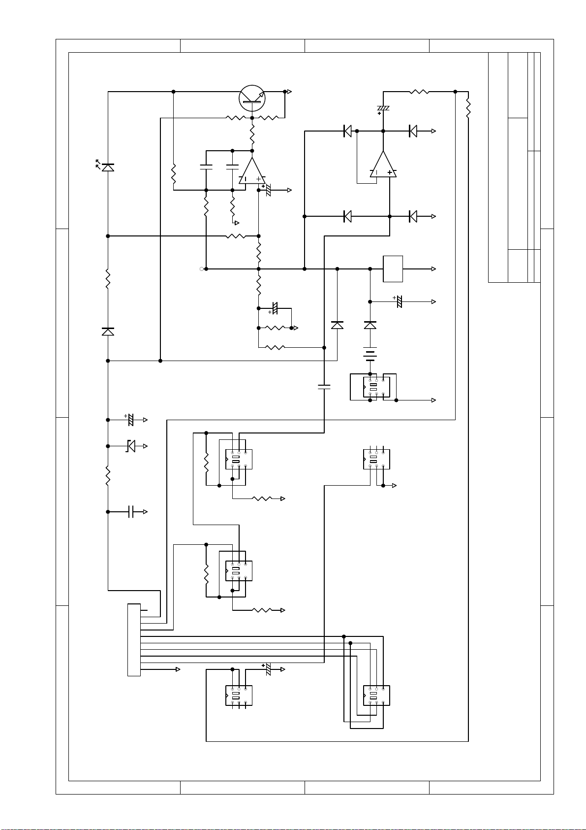
1. SPECIFICATIONS (DI1)
Inputs 1/4” jack unbal. In/ Link Out
XLR unbalanced In
Input Impedance max 220 kOhm
Maximum Input level +2/+22/+42 dBm
Output XLR balanced Out
Load Impedance >600 Ohm
Maximum Output Level +6 dBm
System specifications
Bandwidth(100kOhm) 10Hz to 200Khz(±3dbm)
Bandwidth(600Ohm) 10Hz to 45Khz(±3dbm)
Bandwidth(High Cut) 10Hz to 8Khz(±3dbm)
Noise Level -105 dBm
THD+N @ 1 kHz / 1dBm< 0.01 %
Power supply
Phantom power 18 V DC to 48 V DC
Battery 9 V blockcell 6LR91
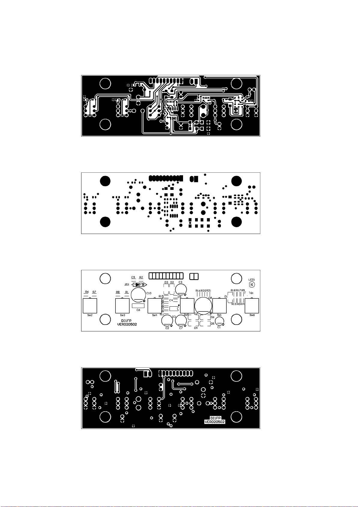
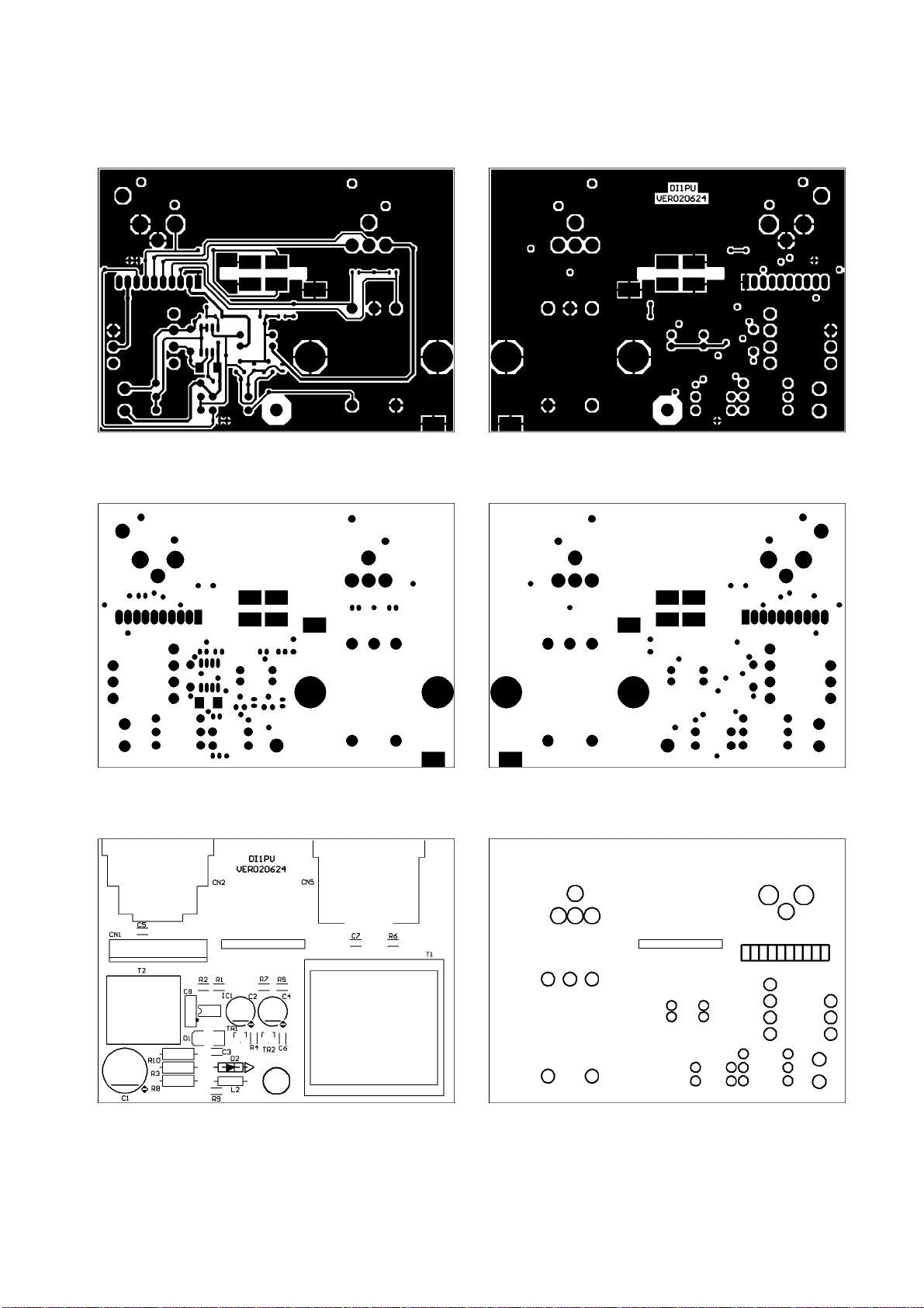
Dimensions 128 mm x 123.5 mm x 44.2 mm
Weight ca. 0.8Kg

1234
A
B
C
D
4321
D
C
B
A
DI1 DIGRAM.Sch
Titel
Size
File:
Date: Drawn By:
Sheet
RevisionModel No:
15-Jun-2002 TASY J.S.
DI1 BLOCK DIGRAM
11 of
DI1 V1.0
A4
INPUT
INPUT
LINK
2
1
3
4
CN2
XLMN-3PH 3c
5e
1a
4d
2b
CN3
CN-JY6351G-02
3c
5e
1a
4d
2b
CN4
CN-JY6351G-02
SW2
-20dB ATTENUATION SW3
-20dB ATTENUATION
LED1
LED CONTROL
SW1
8KHz HIGH CUT 2
1
3
OUTPUTT1 SW4
PHASE
SW5
GND LIFT
SW6
BATTERY POWER
BATTERY +9V
PHANTOM POWER
STEP-DOWN CONVERTER
IC1
2.Block Diagram

1234
A
B
C
D
4321
D
C
B
A
1
2
3
4
5
6
7
8
9
10
CN1
10P-2.0
SW2
PS-22E85L SW3
PS-22E85L
R7
470K
R6
51K
R1
470K
R8
51K
( -20dB ) ( -20dB )
SW4
PS-22E85L
(PHASE)
SW5
PS-22E85L
( GND LIFT )
1
3
4
5
6
2
SW1
PS-22E85L
C1
0.47/50V
(8KHZ HIGH CUT)
LED1
GR
D3
FM103
SW6
DC-POWER
CN2
DC +9V D2
FM103
C7
100u/25v
R5
24K
R18
47K
R19
16K
Q1
BR
R3
47R R17
47K
R4
4K7
R14
16K
D1
4148
R13
100K
R12
100K C2
100u/25v
R16
120K
R15
47K
3
21
IC1A
2068
C5
100n
C4
100n
C3
100u/25v
R11
1M
C6
153 (M)
5
67
IC1B
2068
R21
33R
84
IC1C
2068
D4
4148
D5
4148
C8
470/16V
D6
4148
D7
4148
+VCC
GND2 GND2 GND2
GND2
GND2 GND2
GND2
GND2
GND2 GND2 GND2 GND2 GND2
R20
47R
R2
47R
C9
100n C10
470uF
ZD1
11V
GND2
GND2 GND2 GND2
DI1FP.Sch
Titel
Size
File:
Date: Drawn By:
Sheet
RevisionModel No:
15-Jun-2002 TASY J.S.
DI1FP
11 of
DI1 V1.0
A4
3. Schematic Diagram

1 2 3 4
A
B
C
D
4321
D
C
B
A
R8
1R R3
1R
R1
1K18
C1
470uF
C2
100uF
D1
SFS1B-T
R2
3K32
TR1
BR
TR2
BR
C6
100n
D2
15V
R4
51K
C4
100u/25v
R6
4K7
R7
820R
R5
820R
C7
1n
OUTPUT
1
2
3
4
5
6
7
8
9
10
CN1
10P2.0
R9
22K(omit)
INPUT
INPUT
LINK
L2
220H
2
1
3
4CN5
XLR-3MALE
1
4
2
3
5
T1
OTS-1030
C3
470P
2
1
3
4
CN2
XLMN-3PH 3c
5e
1a
4d
2b
CN3
CN-JY6351G-02
3c
5e
1a
4d
2b
CN4
CN-JY6351G-02
LINK
C5
100P
GND1
GND1GND1
GND1 GND1 GND1
GND1
GND2 GND2
GND2
GND2 GND2 GND2
T2
GND2
C8
104P
R10
27R
IC1
MC34063A/E
1
DI1PU.Sch
Titel
Size
File:
Date: Drawn By:
Sheet
RevisionModel No:
2-Jul-2002 TASY J.S.
DI1PU
11 of
DI1 V1.0
A4

4.Printed Circuit Diagram
DI1FP PCB LAYOUT
PCB : DI1FP Top Layer
PCB : DI1FP Top Solder Mask
PCB : DI1FP Top Overlay
PCB : DI1FP Bottom Layer

PCB : DI1FP Bottom Solder Mask
PCB : DI1FP Bottom Overlay
PCB : DI1FP Drill Drawing Plots
Hole Size Hole Count
24mil (0.6mm) 46
31mil (0.8mm) 54
35mil (0.9mm) 10
39mil (1.0mm) 2
138mil (3.5mm) 4
Totals 116

DI1PU PCB LAYOUT
PCB : DI1PU Top Layer PCB : DI1PU Bottom Layer
PCB : DI1PU Top Solder Mask PCB : DI1PU Bottom Solder Mask
PCB : DI1PU Top Overlay PCB : DI1PU Bottom Overlay

PCB : DI1PU Drill Drawing Plots
Hole Size Hole Count
24mil (0.6mm) 28
31mil (0.8mm) 25
35mil (0.9mm) 10
39mil (1.0mm) 5
47mil (1.2mm) 4
63mil (1.6mm) 8
126mil (3.2mm) 2
150mil (3.8mm) 1
197mil (5.mm) 2
Totals 85

DI4IN PCB LAYOUT
PCB : DI4IN Top Layer PCB : DI4IN Top Solder Mask
PCB : DI4IN Top Overlay PCB : DI4IN Bottom Layer
PCB : DI4IN Bottom Solder Mask PCB : DI4IN Drill Drawing Plots
Hole Size Hole Count
24mil (0.6mm) 2
87mil (2.2mm) 10
Totals 12


1234
A
B
C
D
4321
D
C
B
A
DI1 Wiring DIAGRAM
CN1
CN1
DI1PU
DI1FP
DI1(全).Sch
Titel
Size
File:
Date: Drawn By:
Sheet
RevisionModel No:
26-Oct-2002 TASY J.S
DI1 Wiring DIAGRAM
11 of
DI1 V1.0
A4
CN2
PT-DI1
BATTERY +9V
5. Wiring Diagram

6. Test Procedure
Adjustments (Please follow the instructions to test.)
1. Setting 1
Settings:
1.AP: set same as left features。
Test:
1.LEVEL: Keep it at the range
of +5dBm±1dBm
2.Distortion: 0.01%(+0.005%)。

2. Setting 2.
Setting:
1. Set AP OUTPUT in OFF mode.
Test :
1. Noise Level -105 Bm(±3dBm)

3. Test 3
Settings:
1. AP: Set as the left features.
2. RED Curve shows when all
functions are at “OFF”mode, and
the setting for AP output
impedance is 100K
3. CYAN Curve shows when all
functions are at “OFF”mode, and
the setting for AP output
impedance is 600Ω
4. GREEN curve means only HIGH
CUT(8KHZ) is ON, and AP
output impedance is 600Ω
5. Testing curve should be same as
the curve in the pictures next
page, ±2dBm

Other hints :
1. All function switches (-20dBm,GND LIFT, PHASE) should be tested as well-functions
(1) When -20dBm is pushed down, LEVEL will be reduced to -20 dBm±2dBm
(2) When both -20dBm buttons are pushed down, LEVEL will be reduced to -40
dBm±4dBm
(3) GND (Ground) LIFT button is to separate output and input ground.
2. Phantom power test
(1) aMICTUBE (PHANTOM +48V) can be used to test that if the wire assemblies of DI1,
PIN 9, pass through voltage on 8.5V±0.5V or not.
(2) When you use phantom power, the LED indicator for power is illuminated. However,
if you use battery, then the indicator will flash.
Original settings for products:
1. All functions are in “OFF”mode.
2. Products should pass final test.
Audio Precision
06/28/02 17:55:59
last.at2c
Color Line Style Thick Data Axis
Cyan Solid 2Anlr.Level A Left
Green Solid 2Anlr.Level A Left
Red Solid 2Anlr.Level A Left
-50
+10
-40
-30
-20
-10
+0
d
B
m
20k 200k40k 60k 80k 100k 120k 140k 160k 180k
Hz

DI1-ALTO
Structure Needing Material Detail List
Midprod NO
NO.
Quanity
Unit
建檔日: 2002/07/06 2002/08/09修正日:
Page 1 of 1
2002/10/26
A-DI1-ALTO1 1.000 PCS
A-DI1-底板組合2 1.000 PCS
A-DI1-前板組合3 1.000 PCS
P-DI1FP-SMD4 1.000 PCS
P-DI1FP-DIP5 1.000 PCS
P-DI1PU-SMD6 1.000 PCS
P-DI1PU-DIP7 1.000 PCS
P-DI4IN(DI1)8 1.000 PCS
7. Electrical Parts List

Page 1 of 1
2002/10/26
DI1-ALTO
Mid No: A-DI1-ALTO standard quantity: 1.000
DI1 AMPItem No: specify:
Item Name SpecificNO Material No UnitQuanity Ps
panel
1
MA03379
MARK:
PCS
1.000
DI1 ALTO
top cover
2
MC00424
MARK:
PCS
1.000
DI1
rear board
3
MB02312
MARK:
PCS
1.000
DI1
battery cover
4
MI01412
MARK:
PCS
1.000
DI1
header wiring AF:W141
5
HLSF141
MARK:
PCS
1.000
2P plus 9V battery clip 220m/m
6
NPL287
MARK:
PCS
6.000
φ3*W6*18.3 black ABS
black plated screw
7
MSCB28
MARK:
PCS
5.000
flat self 3*4
DI1FP, DI1PU
black plated screw
8
MSCB38
MARK:
PCS
4.000
3*7
面板
black-plated screw
9
MSCB13
MARK:
PCS
10.000
cross-head pan head 3*6
上蓋,後板,前板
black plated screw
10
MSCB58
MARK:
PCS
4.000
iron-board pill 3*10
平衡座
self-paste foot pad(SF-004)
11
NLXM39
MARK:
PCS
4.000
12.7*9.0*3.0t
PE bag
12
NWCP01WW0200*0220
MARK:
PCS
1.000
20*22cm
lockable bag
13
NWCP04
MARK:
PCS
1.000
5*7
desiccant
14
HEM-002
MARK:
PCS
1.000
10g
MIC stand nut
15
ME00060
MARK:
PCS
2.000
JY-6351G-02-250
mic stand washer
16
MF00061
MARK:
PCS
2.000
JY-6351G-02-250
box
17
NB01832
MARK:
PCS
1.000
DI1 ALTO
instruction
18
NF00968
MARK:
PCS
1.000
DI1 ALTO
assurance book
19
NMCQ-073
MARK:
1.000
ALTO
black plated screw
20
MSCB39
MARK:
PCS
1.000
φ12*14
paper outter case 8hole
21
POA002
MARK:
PCS
0.125
aVERB
EV bubble sponge
22
ND00209
MARK:
PCS
1.000
40*15*5
label
23
NE04366
MARK:
2.000
DI1 ALTO
label
24
NE05004
MARK:
4.000
ALTO
label
25
NE07650
MARK:
PCS
4.000
DI1 機種條碼
Table of contents
Other LTO Music Mixer manuals