Marantz SR5010/U1B User manual

AV SURROUND RECEIVER
SR5010 /U1B/N1B/N1SG
/K1B
SR5010
S0074V02DM/DG1710
Copyright 2017-2015 D&M Holdings Inc. All rights reserved.
WARNING: Violators will be prosecuted to the maximum extent possible.
Ver. 2
•Some illustrations using in this service manual are slightly different from the actual set.
•Please use this service manual with referring to the operating instructions without fail.
•For purposes of improvement, specications and design are subject to change without notice.
Please refer to the
MODIFICATION NOTICE.
Service
Manual

Contents
ABOUT THIS MANUAL................................................................3
What you can do with this manual ...........................................3
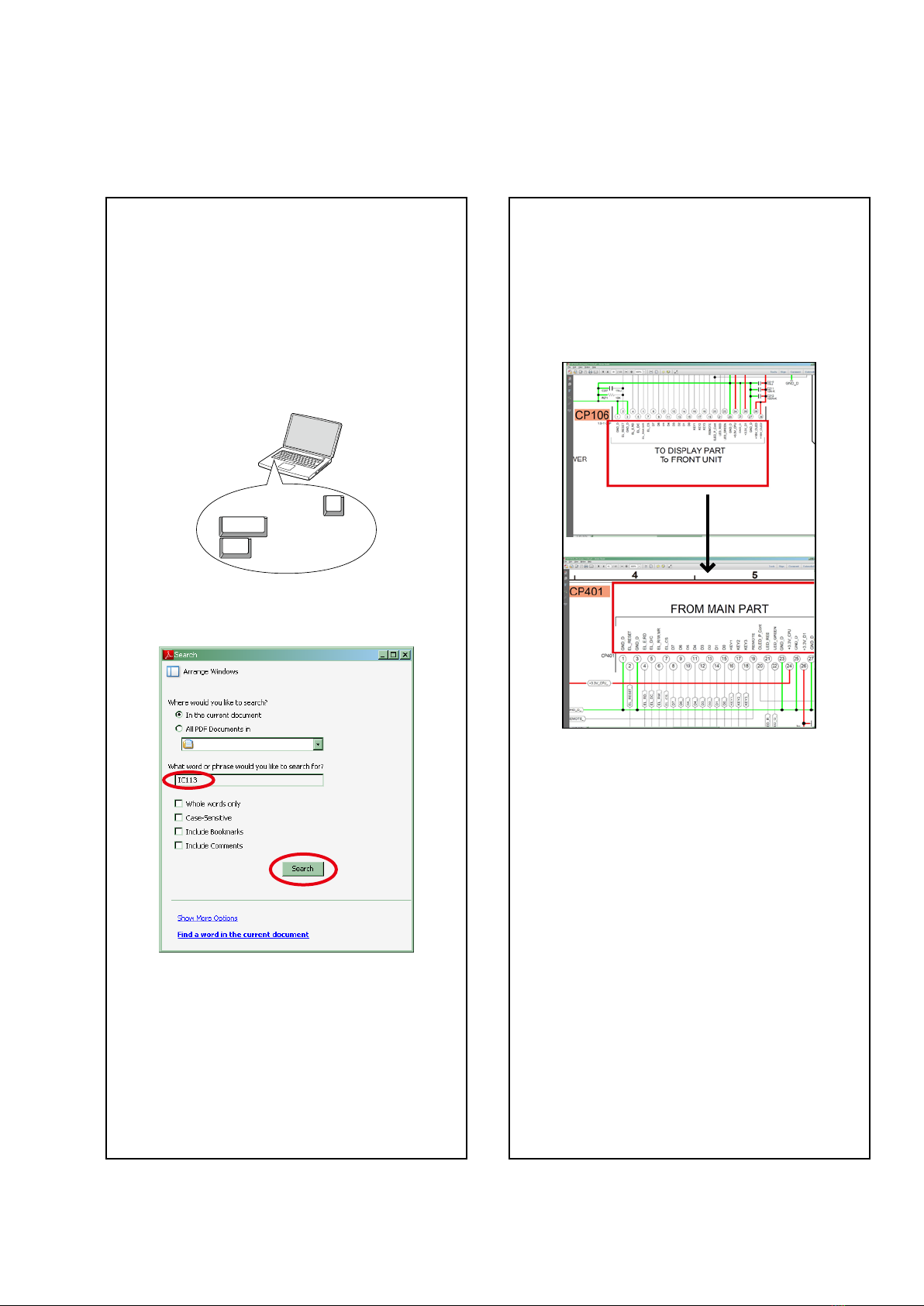
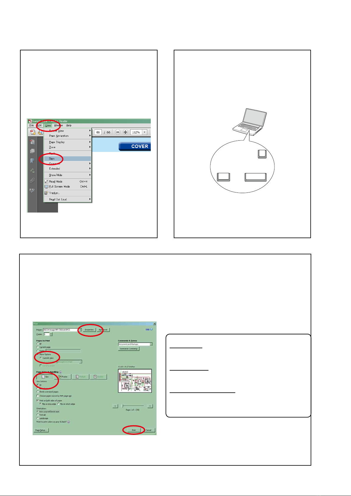
Using Adobe Reader (Windows version)...................................4
SAFETY PRECAUTIONS...............................................................6
NOTE FOR SCHEMATIC DIAGRAM..............................................7
NOTE FOR PARTS LIST................................................................7
TECHNICAL SPECIFICATIONS ....................................................9
DIMENSION ..............................................................................10
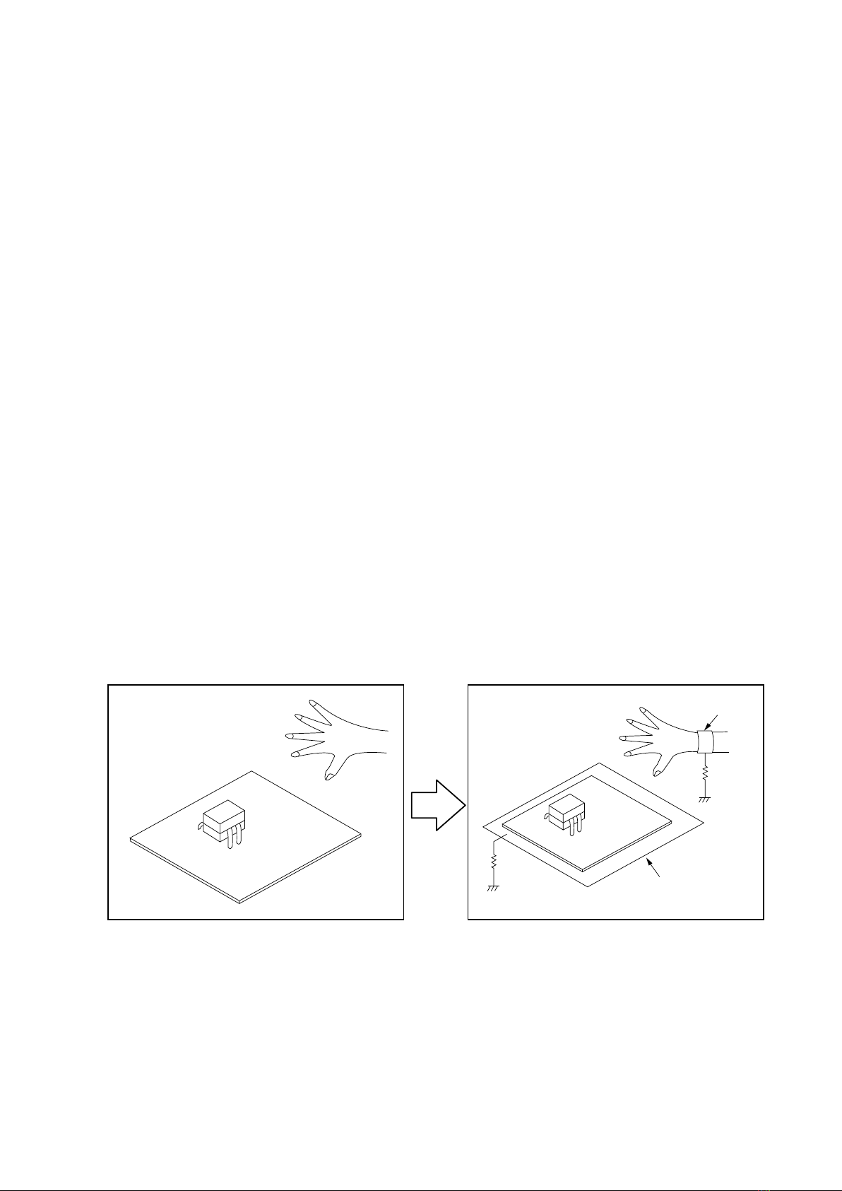
CAUTION IN SERVICING ...........................................................11
Initializing This Unit.................................................................11
JIG FOR SERVICING ..................................................................11
DISASSEMBLY ..........................................................................12
1. FRONT PANEL ASSY............................................................14
2. RADIATOR ASSY .................................................................14
3. HDMI PCB...........................................................................15
4. VIDEO PCB..........................................................................16
5. PREOUT PCB.......................................................................16
6. MAIN PCB...........................................................................17
7. SMPS PCB...........................................................................17
8. TRANS ................................................................................17
SPECIAL MODE.........................................................................18
Special mode setting button ..................................................18
1. Version Display Mode ........................................................19
2. PANEL / REMOTE LOCK Selection Mode ............................22
3. Selecting the Mode for Service-related Operations...........23
DIAGNOSTIC PATH DIAGRAM ............................................26
4. Protection Pass Mode ........................................................48
5. CY920 Reboot Mode ..........................................................48
6. CY920 Initialization Mode ..................................................49
JIG FOR SERVICING ..................................................................50
PROCEDURE AFTER REPLACING THE MICROPROCESSOR, ETC.52
FIRMWARE UPDATE PROCEDURE............................................53
1. Updating via USB ...............................................................53
2. Updating via DPMS ............................................................62
ADJUSTMENT...........................................................................69
SURROUND MODES AND PARAMETERS..................................70
TROUBLE SHOOTING................................................................73
1. POWER ...............................................................................73
2. Analog video......................................................................74
3. HDMI/DVI ...........................................................................78
4. AUDIO ................................................................................80
5. Network / Bluetooth / USB.................................................83
6. SMPS ..................................................................................88
CLOCK FLOW & WAVE FORM IN DIGITAL BLOCK.....................90
LEVEL DIAGRAM.......................................................................91
BLOCK DIAGRAM .....................................................................97
POWER DIAGRAM ..................................................................100
WIRING DIAGRAM..................................................................101
PRINTED WIRING BOARDS.....................................................102
SCHEMATIC DIAGRAMS (01/29).............................................110
SCH01_HDMI SW1 ................................................................110
SCH02_HDMI SW2 ................................................................ 111
SCH03_NET_PHY...................................................................112
SCH04_CPU_LEVEL_CHG......................................................113
SCH05_DIGITAL_CNT............................................................114
SCH06_CPU...........................................................................115
SCH07_FRONT HDMI.............................................................116
SCH08_DSP ...........................................................................117
SCH09_ADV8003...................................................................118
SCH10_ADV8003 DDR...........................................................119
SCH11_D SUPPLY..................................................................120
SCH12_HDMI TX....................................................................121
SCH13_DIR_A PLD ................................................................122
SCH14_MAIN DAC.................................................................123
SCH15_ADV7850...................................................................124
SCH16_INPUT........................................................................125
SCH17_VIDEO .......................................................................126
SCH18_VIDEO_FRONT_CNT..................................................127
SCH19_VIDEO_RC5 ...............................................................128
SCH20_AMP1 ........................................................................129
SCH21_AMP2 ........................................................................130
SCH22_MAIN_SPK.................................................................131
SCH23_MAIN_TUNER_REG ...................................................132
SCH24_MAIN_RS CNT_AUDIO IN..........................................133
SCH25_FRONT.......................................................................134
SCH26_FRONT_RS232...........................................................135
SCH27_SMPS.........................................................................136
SCH28_HDAM.......................................................................137
SCH29_PREOUT.....................................................................138
EXPLODED VIEW ....................................................................139
PACKING VIEW .......................................................................140
SEMICONDUCTORS ................................................................141
1. IC's....................................................................................141
2. FL DISPLAY.......................................................................156
2

Jump to the target of a schematic
diagram connector
Click the Ref. No. of the target connector in the red
box around a schematic diagram connector.
•The screen jumps to the target connector.
•Pagemagnicationstaysthesameasbeforethe
jump.
CP401
CP106
v
ABOUT THIS MANUAL
Read the following information before using the service manual.
What you can do with this manual
Search for a Ref. No. (phrase)
(Ctrl+Shift+F)
You can use the search function in Acrobat Reader to
search for a Ref. No. in schematic diagrams, printed
wiring circuit diagrams, block diagrams, and parts
lists.
1.Press Ctrl+Shift+Fonthekeyboard.
• The Search window appears.
2.EntertheRef.No.youwanttosearchforinthe
Search window, and then click the Search button.
•A list of search results appears.
3.Click an item on the list.
• The screen jumps to the page for that item, and the
searchphraseisdisplayed.
Ctrl
Shift
F
3

Using Adobe Reader (Windows version)
• Properties
Click this button and check that the printer is set to a
suitable paper size.
• Page to print
Select the following checkbox.
"More Options" : "Current View"
• Page Sizing & Handling
Select the following checkbox.
"Size" / "Size Options" : "Fit"
Add notes to this data (Sign)
TheSignfunctionletsyouaddnotestothedatain
this manual.
Savetheleonceyouhavenishedaddingnotes.
[Example using Adobe Reader X]
On the "View" menu, click "Sign".
• The Sign pane appears.
[Example using Adobe Reader 9]
On the "Document" menu, click "Sign".
Magnify schematic / printed circuit
board diagrams - 1
(Ctrl+Space, mouse operation)
Press Ctrl+Spaceonthekeyboardanddragthe
mousetoselecttheareayouwanttoview.
• Theselectedareaismagnied.
• Whenyouwanttomovetheareashown,hold
down Space and drag the mouse.
• Whenyouwanttoshowafullpageview,press
Ctrl+0onthekeyboard.
Ctrl Space
0
Print a magnied part of the manual
ThePropertiesdialogboxandfunctionswillvarydependingonyourprinter.
1. Dragthemousetomagnifythepartyouwanttoprint.
2. On the "File" menu, click "Print".
3. CongurethefollowingsettingsinthePrintdialogbox.
4. Click the Print button to start printing.
4

Magnify schematic / printed circuit
board diagrams - 2
(Pan & Zoom function)
ThePan&Zoomfunctionletsyouseewhichpartof
amagnieddiagramisbeingshowninaseparate
window.
[Example using Adobe Reader X]
On the "View" menu, point to "Zoom", and then click
"Pan & Zoom".
• The Pan & Zoom window appears on the screen.
[Example using Adobe Reader 9]
On the "Tools" menu, point to "Select & Zoom", and
then click "Pan & Zoom Window".
Magnify schematic / printed circuit
board diagrams - 3
(Loupe Tool function)
TheLoupeToolfunctionletsyoumagnifyaspecic
part of a diagram in a separate window.
[Example using Adobe Reader X]
On the "View" menu, point to "Zoom", and then click
"Loupe Tool".
• The Loupe Tool window appears on the screen.
[Example using Adobe Reader 9]
On the "Tools" menu, point to "Select & Zoom", and
then click "Loupe Tool Window".
5

SAFETY PRECAUTIONS
The following items should be checked for continued protection of the customer and the service technician.
leakage current check
Beforereturningthesettothecustomer,besuretocarryouteither(1)aleakagecurrentcheckor(2)alinetochassis
resistance check. If the leakage current exceeds 0.5 milliamps, or if the resistance from chassis to either side of the
power cord is less than 460 kohms, the set is defective.
Be sure to test for leakage current with the AC plug in both polarities, in addition, when the set's power is in each state
(on,offandstandbymode),ifapplicable.
CAUTION Please heed the following cautions and instructions during servicing and
inspection.
◎Heed the cautions!
Cautions which are delicate in particular for servicing
are labeled on the cabinets, the parts and the chassis,
etc. Be sure to heed these cautions and the cautions
described in the handling instructions.
◎Cautions concerning electric shock!
(1) AnACvoltageisimpressedonthisset,soifyou
touch internal metal parts when the set is energized,
youmaygetanelectricshock.Avoidgettingan
electricshock,byusinganisolatingtransformer
and wearing gloves when servicing while the set is
energized,orbyunpluggingthepowercordwhen
replacing parts, for example.
(2) Therearehighvoltagepartsinside.Handlewith
extra care when the set is energized.
◎Caution concerning disassembly and
assembly!
Through great care is taken when parts were
manufacturedfromsheetmetal,theremaybeburrson
theedgesofparts.Theburrscouldcauseinjuryifngers
are moved across them in some rare cases. Wear gloves
toprotectyourhands.
◎Use only designated parts!
Theset'spartshavespecicsafetyproperties(re
resistance,voltageresistance,etc.).Besuretouseparts
which have the same properties for replacement. The
burrs have the same properties. In particular, for the
importantsafetypartsthatareindicatedbythezmark
on schematic diagrams and parts lists, be sure to use
the designated parts.
◎Be sure to mount parts and arrange the wires
as they were originally placed!
Forsafetyseasons,somepartsusetapes,tubesorother
insulatingmaterials,andsomepartsaremountedaway
from the surface of printed circuit boards. Care is also
takenwiththepositionsofthewiresbyarrangingthem
andusingclampstokeepthemawayfromheatingand
highvoltageparts,sobesuretoseteverythingbackas
itwasoriginallyplaced.
◎Make a safety check after servicing!
Check that all screws, parts and wires removed or
disconnected when servicing have been put back in their
original positions, check that no serviced parts have
deteriorate the area around. Then make an insulation
check on the external metal connectors and between
the blades of the power plug, and otherwise check that
safetyisensured.
(Insulationcheckprocedure)
Unplug the power cord from the power outlet, disconnect
the antenna, plugs, etc., and on the power. Using a 500V
insulation resistance tester, check that the insulation
resistancevaluebetweentheinplugandtheexternally
exposedmetalparts(antennaterminal,headphones
terminal,inputterminal,etc.)is1MΩorgreater.Ifitis
less, the set must be inspected and repaired.
Manyoftheelectricandthestructuralpartsusedinthe
sethavespecialsafetyproperties.Inmostcasesthese
propertiesaredifculttodistinguishbysight,andtheuse
ofreplacementpartswithhigherratings(ratedpower
andwithstandvoltage)doesnotnecessarilyguarantee
thatsafetyperformancewillbepreserved.Partswith
safetypropertiesareindicatedasshownbelowonthe
wiring diagrams and the parts list in this service manual.
Be sure to replace them with the parts which have the
designated part number.
(1) Schematicdiagrams.......Indicatedbythez mark.
(2) Partslists.......Indicatedbythezmark.
The use of parts other than the
designated parts could cause electric
shocks,resorotherdangerous
situations.
CAUTION Concerning important
safety parts
6

NOTE FOR SCHEMATIC DIAGRAM
WARNING:
Partsindicatedbythezmarkhavecriticalcharacteristics.UseONLYreplacementpartsrecommendedbythemanufacturer.
CAUTION:
Beforereturningthesettothecustomer,besuretocarryouteither(1)aleakagecurrentcheckor(2)alinetochassisresistancecheck.
If the leakage current exceeds 0.5 milliamps, or if the resistance from chassis to either side of the power cord is less than 460 kohms, the
set is defective.
WARNING:
DONOTreturnthesettothecustomerunlesstheproblemisidentiedandremedied.
NOTICE:
ALLRESISTANCEVALUESINOHM.k=1,000OHM/M=1,000,000OHM
ALLCAPACITANCEVALUESAREEXPRESSEDINMICROFARAD,UNLESSOTHERWISEINDICATED.PINDICATESMICRO-MICRO
FARAD.EACHVOLTAGEANDCURRENTAREMEASUREDATNOSIGNALINPUTCONDITION.CIRCUITANDPARTSARESUBJECT
TOCHANGEWITHOUTPRIORNOTICE.
NOTE FOR PARTS LIST
1.Partsindicatedby"nsp" on this table cannot be supplied.
2.Whenorderingapart,makeacleardistinctionbetween"1"and"I"(i)toavoidmis-supplying.
3.Apartorderedwithoutspecifyingitspartnumbercannotbesupplied.
4.Partindicatedby" ★" mark is not illustrated in the exploded view.
WARNING:Partsindicatedbythezmarkhavecriticalcharacteristics.UseONLYreplacementpartsrecommendedbythemanufacturer.
INSTRUCTIONS FOR HANDLING SEMI-CONDUCTORS AND OPTICAL UNIT
Electrostaticbreakdownofthesemi-conductorsoropticalpickupmayoccurduetoapotentialdifferencecausedby
electrostatic charge during unpacking or repair work.
1. GroundforHumanBody
Besuretowearagroundingband(1MΩ)thatisproperlygroundedtoremoveanystaticelectricitythatmaybe
chargedonthebody.
2. GroundforWorkbench
Besuretoplaceaconductivesheetorcopperplatewithpropergrounding(1MΩ)ontheworkbenchorothersurface,
wherethesemi-conductorsaretobeplaced.Becausethestaticelectricitychargeonclothingwillnotescapethrough
thebodygroundingband,becarefultoavoidcontactingsemi-conductorswithyourclothing
<Incorrect>
CBA
Grounding Band
Conductive Sheet or
Copper Plate
1MΩ
1MΩ
<Correct>
CBA
7

Personal notes:
8

TECHNICAL SPECIFICATIONS
nAudio section
• Power amplier
Rated output :
Front :
100 W + 100 W ( 8 Ω, 20 Hz - 20 kHz with 0.08 % T.H.D.)
140 W + 140 W ( 6 Ω, 1 kHz with 0.7 % T.H.D.)
Center :
100 W ( 8 Ω, 20 Hz - 20 kHz with 0.08 % T.H.D.)
140 W ( 6 Ω, 1 kHz with 0.7 % T.H.D.)
Surround :
100 W + 100 W ( 8 Ω, 20 Hz - 20 kHz with 0.08 % T.H.D.)
140 W + 140 W ( 6 Ω, 1 kHz with 0.7 % T.H.D.)
Surround back :
100 W + 100 W ( 8 Ω, 20 Hz - 20 kHz with 0.08 % T.H.D.)
140 W + 140 W ( 6 Ω, 1 kHz with 0.7 % T.H.D.)
Output connectors : 4 - 16 Ω
nAnalog section
Input sensitivity/Input impedance : 200 mV / 47 kΩ
Frequency response : 10 Hz - 100 kHz — +1, -3 dB (Direct mode)
S/N ratio : 100 dB (IHF-A, Direct mode)
nVideo section
• Standard video connectors
Input/output level and impedance : 1 Vp-p, 75 Ω
Frequency response : 5 Hz - 10 MHz — 0, –3 dB
• Color component video connector
Input/output level and impedance : Y signal — 1 Vp-p, 75 Ω
PB / CB signal — 0.7 Vp-p, 75 Ω
PR / CR signal — 0.7 Vp-p, 75 Ω
Frequency response : 5 Hz - 60 MHz — 0, –3 dB
nTuner section
(Note : μV at 75 Ω, 0 dBf = 1 x 10 –15 W)
Reception frequency range : FM 87.5 MHz - 107.9 MHz (for U)
FM 87.5 MHz - 108.0 MHz (for N, K)
AM 520 kHz - 1710 kHz (for U)
AM 522 kHz - 1611 kHz (for N, K)
Effective sensitivity : FM 1.2 μV (12.8 dBf)
AM 18 μV
50 dB sensitivity : MONO―2.8μV(20.2dBf)
S/N ratio (IHF-A) : MONO ― 70 dB (for U)
MONO ― 78 dB (for N, K)
STEREO ― 67 dB (for U)
STEREO ― 67 dB (for N, K)
Distortion : MONO ― 0.7 % (for U)
MONO ― 0.7 % (1 kHz) (for N, K)
SRETEO ― 1.0 % (for U)
SRETEO ― 1.0 % (1 kHz) (N, K)
nWireless LAN section
Network type (wireless LAN standard) : Conforming to IEEE 802.11b
Conforming to IEEE 802.11g
Conforming to IEEE 802.11n
(Wi-Fi® compliant)z1
Security : WEP 64 bit, WEP 128 bit
WPA/WPA2-PSK (AES)
WPA/WPA2-PSK (TKIP)
Radio frequency : 2.4 GHz
No. of channels : 1 - 11 ch (for U)
1 - 13 ch (for N, K)
z1 The Wi-Fi® CERTIFIED Logo and the Wi-Fi CERTIFIED On-Product Logo
are registered trademarks of the Wi-Fi Alliance.
nBluetooth section
Communications system : Bluetooth Version 2.1 + EDR
(Enhanced Data Rate)
Transmission power : Maximum 2.5 mW (Class 2)
Maximum communication range : Approx. 32.8 ft/10 m in line of sight *2
Frequency band : 2.4 GHz band
Modulation scheme : FHSS (Frequency-Hopping Spread Spectrum)
Supported proles : A2DP (Advanced Audio Distribution Prole)1.2
AVRCP (Audio Video Remote Control Prole)1.4
Corresponding codec : SBC, AAC
Transmission range (A2DP) : 20Hz-20,000Hz
z2 The actual communication range varies depending on the inuence of
such factors as obstructions between devices, electromagnetic waves
from microwave ovens, static electricity, cordless phones, reception
sensitivity, antenna performance, operating system, application
software etc.
nGeneral
Power supply : (for U) : AC 120 V, 60 Hz
(for N) : AC 230 V, 50 Hz / 60 Hz
(for K) : AC 220 V, 50 Hz
Power consumption : 650 W
Power consumption in standby mode : 0.2 W
Power consumption in CEC standby mode : 0.5 W
Power consumption in network standby mode : 2.7 W
For purposes of improvement, specications and design are subject to
change without notice.
9

6 1/2 (165)
2 1/2
(64)
2 11/16
(69)
17 5/16 (440)
1/2
(13)
5 13/16 (148)
6 5/16 (161)
9 1/16 (230)
11 3/4 (298)
13 5/8 (346)
5/8
(16)
1 1/4
(32)
13 3/8 (340) )05(61/511)05(61/511
2 3/16
(55)
DIMENSION
Unit : in. (mm)
Weight : 22 lb 1 oz (10 kg)
10

CAUTION IN SERVICING
Initializing This Unit
Make sure to initialize this unit after replacing the microcomputer or any peripheral equipment, or the digital PCB.
1. Press the power button to turn off the power.
2. While holding down buttons "TUNER PRESET CH -" and "TUNER PRESET CH +" simultaneously, press the power
button to turn on the power.
3. Release the buttons after conrming that the display ashes at 1-second intervals.
* The unit is initialized.
NOTE:• If the unit fails to enter the service mode in step 3, repeat the procedure from step 1.
• Initializing the device restores the customized settings to the factory settings. Write down your settings in advance and
recongure the settings after initialization.
JIG FOR SERVICING
Use the following jigs (extension cable kit) when repairing the PCBs.
Order with your dealer for the jigs your dealer if necessary.
8U-110084S : EXTENSION UNIT KIT : 1 Sets
8U-110136S : EXTENSION UNIT KIT : 1 Sets
(See page 50)
TUNER
PRESET CH +
TUNER
PRESET CH -
X
11

FRONT PANEL ASSY
See "DISASSEMBLY"
1. FRONT PANEL ASSY
and "EXPLODED VIEW"
H/P PCB
Ref. No. of EXPLODED VIEW : P 1
FRONT HDMI PCB
Ref. No. of EXPLODED VIEW : P 2
USB PCB
Ref. No. of EXPLODED VIEW : P 3
FRONT PCB
Ref. No. of EXPLODED VIEW : P 4
F/H_GUIDE PCB
Ref. No. of EXPLODED VIEW : P 11
TOP COVER
TRANS
See "DISASSEMBLY"
8. TRANS
and "EXPLODED VIEW"
POWER TRANS
Ref. No. of EXPLODED VIEW : P 31
RADIATOR ASSY
See "DISASSEMBLY"
2. RADIATOR ASSY
and "EXPLODED VIEW"
AMP PCB
Ref. No. of EXPLODED VIEW : P 8
GUIDE L PCB
Ref. No. of EXPLODED VIEW : P 10
TOP_GUIDE PCB
Ref. No. of EXPLODED VIEW : P 9
HDMI PCB
See "DISASSEMBLY"
3. HDMI PCB
and "EXPLODED VIEW"
HDMI PCB
Ref. No. of EXPLODED VIEW : P 16
VIDEO PCB
See "DISASSEMBLY"
4. VIDEO PCB
and "EXPLODED VIEW"
VIDEO PCB
Ref. No. of EXPLODED VIEW : P 19
PREOUT PCB
See "DISASSEMBLY"
5. PREOUT PCB
and "EXPLODED VIEW"
PREOUT PCB
Ref. No. of EXPLODED VIEW : P 20
MAIN PCB
See "DISASSEMBLY"
6. MAIN PCB
and "EXPLODED VIEW"
MAIN PCB
Ref. No. of EXPLODED VIEW : P 12
INPUT PCB
Ref. No. of EXPLODED VIEW : P 13
HDAM PCB
Ref. No. of EXPLODED VIEW : P 7
HDAM CNT PCB
Ref. No. of EXPLODED VIEW : P 6
SMPS PCB
See "DISASSEMBLY"
7. SMPS PCB
and "EXPLODED VIEW"
SMPS PCB
Ref. No. of EXPLODED VIEW : P 18
DISASSEMBLY
• Remove each part following the ow below.
• Reassemble the removed parts in the reverse order.
• Read "Precautions During Work"before reassembling the removed parts.
• If wire bundles are removed or moved during adjustment or part replacement, reshape the wires after completing
the work. Failure to shape the wires correctly may cause problems such as noise.
12

Explanatory Photos for DISASSEMBLY
• For the shooting direction of each photos used in this manual, see the photo below.
• A, B, C and D in the photo below indicate the shooting directions of photos.
• The photographs with no shooting direction indicated were taken from the top of the unit.
• Photos of SR5010 N1SG are used in this manual.
The viewpoint of each photograph
(Shooting direction : X) [View from the top]
Front side
Shooting
direction: D
Shooting
direction: C
↑Shooting direction: A↑
↓Shooting direction: B↓
13

1. FRONT PANEL ASSY
Proceeding : TOP COVER →FRONT PANEL ASSY
(1) Remove the screws.
(2) Remove the screws. Remove the CORD HOLDERs and the connector wires. Remove the FFC.
2. RADIATOR ASSY
Proceeding : TOP COVER →FRONT PANEL ASSY →RADIATOR ASSY
(1) Remove the screws.
(2) Remove the CORD HOLDERs and connector wires.
View from the bottom
x8
FFC FFC
N1008
CP4400
CORD HOLDER
View from the bottomShooting direction: C Shooting direction: D
x7
CP405CP403CP402
CP401
CORD HOLDER
14

3. HDMI PCB
Proceeding : TOP COVER →BACK CHASSIS →HDMI PCB
(1) Remove the screws.
(2) Cut the wire clamps, and then remove the CORD HOLDERs and the connector wires. Remove the FFC.
(3) Cut the wire clamp and remove the connector.
Shooting direction: A x12
x32
x2 x2
FFC FFC
N1008
N1033
CORD HOLDER x 5
CUT
N1039N1019
N1014
N1016
N1020
CUT
15

4. VIDEO PCB
Proceeding : TOP COVER →BACK CHASSIS →HDMI PCB →VIDEO PCB
(1) Remove the connector.
5. PREOUT PCB
Proceeding : TOP COVER →BACK CHASSIS →HDMI PCB →VIDEO PCB →PREOUT PCB
(1) Remove the connectors.
CN5000
CN5000
CN5601
CN5602
CN4704
TO CP401
16

6. MAIN PCB
Proceeding : TOP COVER →BACK CHASSIS →HDMI PCB →VIDEO PCB →PREOUT PCB →MAIN PCB
(1) Remove the screws.
(2) Remove the screws.
7. SMPS PCB
Proceeding : TOP COVER →SMPS PCB
See "EXPLODED VIEW" for instructions on removing the SMPS PCB.
8. TRANS
Proceeding : TOP COVER →HDMI PCB →TRANS
See "EXPLODED VIEW" for instructions on removing the transformer (TRANS).
View from the bottom
x3
x8
x2
from CP405
from CP403CP402
CP401
CP5003
17

SPECIAL MODE
Special mode setting button
b No. 1 - 6, 9 : While holding down buttons "A", "B" and "C" simultaneously, press the power button to turn on the power.
b No. 7, 8 : While the power is on, hold down buttons "A" and "B" for at least 3 seconds .
b No. 10 : While holding down buttons "A" and "B" simultaneously, insert the AC plug into the wall outlet to turn on the power.
No. Mode Button A Button B Button C Descriptions
1Version Display
(u-COM / DSP Error Display) DIMMER STATUS -
Displays the version of rmware such as the main rmware or DSP.
Errors that have occurred are displayed.
(See page 19)
2Selecting the Mode for Service-related ZONE2
SOURCE STATUS - This is a display for turning on each service-related mode.
Service-related modes: No. 2-1 - No. 2-5
2-1 Protection history display mode
TUNER
PRESET CH
+
- - Displays the protection occurrence history.
(See page 44)
2-2 Check the Video/Audio path Mode ↑ - -
This is a special mode for service conrmation used during repair
work to simplify the conrmation work for the Audio channel /
video channel.
(See page 24)
2-3 TUNER STEP Mode
(U and N model only) ↑ - - Enables reception STEP of the ANALOG TUNER to be changed.
(See page 47)
2-4 Operation Info Mode ↑ - -
Displays the accumulated operating time of the unit, the number
of times the power was switched on, and the number of occur-
rences of each protection.
(See page 46)
3User Initialization Mode M-DAX ZONE2
SOURCE -Initializes backup data.
(Settings for the Installer Setup are not initialized.)
4Factory Initialization Mode
TUNER
PRESET CH
-
TUNER
PRESET CH
+
-Initializes backup data.
(The settings for the Installer Setup is also initialized.)
5PANEL / REMOTE LOCK Selection Mode M-DAX DIMMER -
Start this unit in the PANEL/REMOTE LOCK selection mode so that
PANEL LOCK and Remote Lock can be switched between ON and
OFF.
(See page 22)
6Protection Pass Mode DIMMER STATUS SOUND
MODE
Enables the power to be turned on when protection detection is
disabled.
(See page 48)
7CY920 Reboot Mode
TUNER
PRESET CH
+
STATUS - The CY920 is restarted after CY920 hang up.
8CY920 Initialization Mode
TUNER
PRESET CH
-
DIMMER - Enter this mode only after replacing Flash for CY920 and rewriting
the rmware.
9USB Update Mode
TUNER
PRESET CH
+
STATUS - Switches this unit to USB Update mode.
10 Forced USB All Device Write Mode
TUNER
PRESET CH
+
STATUS -
Mode used when this unit cannot be recovered.
Forcibly switches this unit to USB update mode.
(See page 55)
TUNER
PRESET CH +
DIMMER
STATUS
SOUND
MODE
TUNER
PRESET CH -
ZONE2
SOURCEM-DAXX
18

1. Version Display Mode
1.1. Actions
Version information is displayed when the device is started in this mode.
1.2. Starting up
While holding down buttons "DIMMER" and "STATUS" simultaneously, press the power button to turn on the power.
then press the "STATUS" button to display the information in section 1.3 on the display.
b The version list is also displayed on GUI while the version is displayed on the display.
1.3. Display Order
Error information("See 1.4. Error display") → q Model destination information → w Firmware Package Version
→ e Main µ-com → r Main 1st Boot Loader → t DSP ROM → y Audio PLD → u GUI SFLASH
→ i Ethernet 1st Boot Loader, Hardware ID → o Ethernet 2nd Boot Loader, Rhapsody Flag → Q0 Ethernet IMAGE
→ Q1 Ethernet MAC ADDRESS information → Q2 BT MAC Address information
q Model destination information :
FLD
L1 S R 5 0 1 0 U
L2 SN-****
L3 ******
FLD L1 SR5010 N
FLD L1 SR5010 K
w Firmware Package Version:
FLD
L1 PACKAGE
L2
L3 ****
e Main µ-com Version information :
FLD
L1 MAIN *
L2 ****
L3 BL-**.**
r Main 1st Boot Loader :
FLD
L1 MAIN *
L2 ********
L3 BL-**.**
t DSP ROM :
FLD
L1 DSP
L2
L3 **.**
y Audio PLD :
FLD
L1 A.PLD
L2
L3 **.**
u GUI SFLASH :
FLD
L1 G U I
L2 XXYZ****
L3
X
:
Model code, Y
:
Model, Z
:
Region
o Ethernet 1st Boot Loader, Hardware ID :
FLD
L1 N E T F B L
L2 ******
L3 - * *
o Ethernet 2nd Boot Loader, Rhapsody Flag :
FLD
L1 N E T S B L
L2 ********
L3 *****-**
Q0 Ethernet IMAGE :
FLD
L1 N E T I M G
L2 ********
L3 *****
Q1 Ethernet MAC ADDRESS information:
FLD
L1 N E T M A C
L2 ******
L3 -******
Q2 BT MAC ADDRESS information:
FLD
L1 BT MAC
L2 ******
L3 -******
19

1.4. Error display
See the table below for descriptions of the displayed errors and countermeasures for these.
If multiple errors occur, only one item is displayed.
The priority order is w, e, r, t, y, q.
Condition States Display TROUBLE SHOOTING
q
Firm Check
NG
The model name, brand name and region infor-
mation written in the rmware are compared
to the region settings in the PCB. This error is
displayed if the information does not match.
" ▲ " or " ▼ " is displayed as the rst character if
the rmware is not correct (see the illustrations
on the right).
FLD
L1 F I R M
L2 ERROR
L3
FLD
L1 M A I N
–
L2 ********
L3 BL-**.**
FLD
L1 S U B
–
L2 XXYZ****
L3 BL-**.**
FLD
L1 D S P
–
L2
L3 * * . * *
FLD
L1 A . P L D
–
L2
L3 * * . * *
FLD
L1 G U I
–
L2
L3 * * . * *
• Check the resistor for
setting the region(R1524 /
1525 HDMI PCB).
• Write the rmware for the
correct region.
w
IP SCALER NG
An error occurs in Loopback Test of the DDR
memory which is performed during the initial
setting of i/p Scaler (ADV8003).
FLD
L1 I P
L2 SCALER
L3 E R R 0 1
• Check the circuits around
the IP SCALER (U1026,
HDMI PCB) and DDR2
(U1028/1029).
If there appear to be
no problems, U1026 or
U1028/1029 is faulty.
During the initial setting of i/p Scaler ( ADV8003
) , there is not the reply of the Loopback Test
result of the DDR memory .
FLD L3 E R R 0 2
e
GUI Serial
Flash NG
If the Main CPU version is not supported by the
GUI Serial Flash (ADV8003), FLD
L1 G U I V E R .
L2 ERROR
L3
• Check the rmware version.
r
DIR NG
This error is displayed if there is no response
from the DIR. FLD
L1 D I R
L2 ERROR
L3 0 1
• Check the DIR (U1040,
HDMI PCB) and surrounding
circuits.
t
DSP NG
The DSP FLAG0 port does not enter "Hi" status
while booting a DSP code even after resetting
DSP.
FLD
L1 D S P
L2 ERROR
L3 0 1
• Check the DSP (U1073,
HDMI PCB) and surrounding
circuits.
The DSP FLAG0 port does not enter "Hi" status
before issuing a DSP command. FLD L3 0 2
Setting WRITE to "Lo" does not set ACK to "Hi"
during DSP data reading. FLD L3 0 3
Setting REQ to "Lo" does not set ACK to "Lo"
during DSP data reading. FLD L3 0 4
Setting WRITE to "Hi" does not set ACK to "Hi"
during DSP data writing. FLD L3 0 5
Setting REQ to "Lo" does not set ACK to "Lo"
during DSP data writing. FLD L3 0 6
y
EEPROM NG
An error occurred in a checksum of the EE-
PROM(*** is a block address number). FLD
L1 E 2 P R O M
L2 ERROR
L3 * * *
20
This manual suits for next models
3
Table of contents
Other Marantz Stereo Receiver manuals

Marantz
Marantz SR9600U User manual

Marantz
Marantz NR1200 User manual

Marantz
Marantz SR5008 User manual

Marantz
Marantz SR7011 User manual

Marantz
Marantz NR1504 User manual

Marantz
Marantz SR7400 User manual

Marantz
Marantz 2270 User manual

Marantz
Marantz SR5013 User manual

Marantz
Marantz SR5600 User manual

Marantz
Marantz SR5015 DAB User manual

Marantz
Marantz NR1711 User manual

Marantz
Marantz SR5011 User manual

Marantz
Marantz 2238B User manual

Marantz
Marantz SR5012 User manual

Marantz
Marantz SR5007 User manual

Marantz
Marantz SR7013 User manual

Marantz
Marantz SR5003 User manual

Marantz
Marantz SR5500 User manual

Marantz
Marantz 2225L User manual

Marantz
Marantz SR7300 User manual