Maxim MAX3296 User manual

General Description
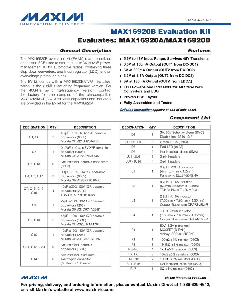
The MAX3296 longwave (LW) evaluation kit (EV kit) is
an assembled, surface-mount demonstration board that
provides easy optical and electrical evaluation of the
MAX3286 1.25Gbps laser driver or the MAX3296
2.5Gbps laser driver in the common-anode configura-
tion. This kit allows evaluation of the MAX3286/MAX3296
with long-wavelength laser diodes. Long-wavelength
(1310nm and greater) laser diodes are typically pack-
aged with their anode connected to a photodetector’s
cathode.
Refer to the MAX3296EVKIT-SW for evaluation of the
MAX3286/MAX3296 with short-wavelength laser diodes
and VCSELs.
Features
♦Drives Common-Anode Lasers
♦Includes Socket for Laser Insertion
♦LED Fault Indicator
♦Evaluates Either MAX3286 or MAX3296 (installed)
♦Adjustable Laser Bias Current
♦Adjustable Laser Modulation Current
♦Adjustable Laser Modulation Current Tempco
♦Configured for Electrical Operation, No Laser
Necessary
Evaluates: MAX3286/MAX3296
MAX3296 Longwave (Common Anode)
Evaluation Kit
________________________________________________________________ Maxim Integrated Products 1
19-1643; Rev 1; 6/00
Component List
PART
MAX3296CGIL 0°C to +70°C
TEMP. RANGE IC PACKAGE
28 QFN
Open, user-supplied (laser diode and
photodiode assembly, see Figure 1)
0D2
10µF ±10%, 16V tantalum capacitor
AVX TAJC106K016
1C24
Open, user-supplied (0402)*0C18
DESIGNATION
0.1µF ±10%, 10V min, X7R ceramic
capacitor (0603)
1C17
0.01µF ±10%, 10V min, X7R ceramic
capacitors (0402)
11
C6–C10, C15,
C16, C21, C27,
C28, C29
DESCRIPTIONQTY
Ferrite bead
Murata BLM11HA601SG
1L7
Ferrite bead (included but not installed)
Murata BLM11HA102SG
1L5
Ferrite beads
Murata BLM11HA102SG
2L3, L6
Red LED1D4
0Ω±5% resistor (0402)1R1
Test points
Digi-Key 5000K-ND
10
TP5–TP8, TP11,
TP12, TP13,
TP16, TP17,
TP18
Test points
Digi-Key 5000K-ND
2J9, J10
2-pin headers (0.1in centers)
Digi-Key S1012-36-ND
5JU6–JU10
SMA connectors (edge mount)
EFJohnson 142-0701-801 or
Digi-Key J502-ND
3J3, J4, J6
1kΩ±5% resistor (0402)1R28
6.8Ω±5% resistor (0402)1R27
511Ω±1% resistor (0402)1R26
MAX4322EUK (5-pin SOT23)1U4
MAX3286CHJ (32-pin TQFP, included
but not installed)
1U3**
MAX3296CHJ (32-pin TQFP)1U3**
Zetex FMMT491A1Q6
Zetex FMMT591A1Q5
49.9Ω±1% resistor (0402)1R19
24.9Ω±1% (0402)*1R17
36Ω±5% resistor (0603)1R15
DESIGNATION
50kΩvariable resistor
Bourns or Digi-Key 3296W-503-ND
1R8
DESCRIPTIONQTY
100kΩvariable resistors
Bourns or Digi-Key 3296W-104-ND
2R7, R14
Ordering Information
18Ω±5% resistor (0402)1R16
36Ω±5% resistor (0402)1R29
115Ω±1% resistor (0402)1R6
MAX3296EVKIT-LW 0°C to +70°C 32 TQFP
MAX3296CGI (28-pin QFN)1U1**
MAX3286CGI (28-pin QFN, included
but not installed)
1U1**
For pricing, delivery, and ordering information, please contact Maxim/Dallas Direct! at
1-888-629-4642, or visit Maxim’s website at www.maxim-ic.com.

Evaluates: MAX3286/MAX3296
MAX3296 Longwave (Common Anode)
Evaluation Kit
2 _______________________________________________________________________________________
Component List (continued)
*These components are part of the compensation network, which
reduces overshoot and ringing. Parasitic series inductance intro-
duces a zero into the laser’s frequency response.
R17 and C18 add a pole to cancel this zero. The optimal values
depend upon the laser used. Maxim recommends R17 = 24.9Ω
and C18 = 2pF as a starting point.
**The MAX3296/MAX3286CHJ parts are included with the
MAX3296EV-KIT-LW. The MAX3296/MAX3286CGI parts are
included with the MAX3296CGIL.
Electrical Quick Start
Electrical Quick Start with
Simulated Photodiode Feedback
1) Short shunts SP1 and SP2 to use the photodiode
emulator circuitry (see Emulating a Photodiode
During Electrical Evaluation).
2) Make sure nothing is installed in the laser socket
(Figure 1).
3) Confirm that R27 is installed.
4) Make sure L5 is not installed.
5) Confirm that C18 is open. Since the laser is not
installed, no compensation network is required.
6) Set potentiometer R14 (RSET) to midscale by turn-
ing the screw clockwise until a faint click is felt,
then counterclockwise for 15 full revolutions (30 full
revolutions in the 0Ωto 100kΩrange of the multi-
turn potentiometer). This sets the regulation point
for the simulated photodiode current to 1.7V / 50kΩ
= 34µA. The photodiode emulator circuit regulates
the DC bias current into Q6 to 28 ·34µA ≅1mA.
7) Set potentiometer R8 (RMOD) to maximum resis-
tance by turning the screw counterclockwise until a
faint click is felt (30 full revolutions in the 0Ωto
50kΩrange of the multiturn potentiometer). This
minimizes the modulation current.
8) Set potentiometer R7 (RTC) to maximum resistance
by turning the screw counterclockwise until a faint
click is felt (30 full revolutions in the 0Ωto 100kΩ
range of the multiturn potentiometer). This mini-
mizes the temperature coefficient (tempco) of the
modulation current.
9) Place jumpers across JU7 (EN), JU8 (EN), and JU9
(PORDLY).
10) If you intend to power the board from a +5V supply,
place a jumper across JU6 (LV). Do not apply
power yet.
11) Make sure there is no jumper on JU10 (FLTDLY).
This enables the safety circuitry.
12) Attach a cable with 50Ωcharacteristic impedance
between the J6 SMA output connector and the
input of the oscilloscope. Make sure the oscillo-
scope input is 50Ωterminated.
13) Attach differential sources to SMA connectors J3
and J4. Each source should have a peak-to-peak
amplitude between 100mV and 830mV.
14) Apply either +3.3V or +5V power to the board at the
J9 (VCC) and J10 (GND) test points. Set the current
limit to 300mA.
15) While monitoring the voltage between TP17 and
TP18, adjust R14 (RSET) until the desired DC bias
current is obtained. Turning the R14 potentiometer
screw counterclockwise increases the DC bias cur-
rent.
16) While monitoring the J6 SMA connector output on
the oscilloscope, adjust R8 (RMOD) until the desired
modulation current is obtained. Turning the R8
potentiometer screw clockwise increases the modu-
lation current.
Emulating a Photodiode During
Electrical Evaluation
When evaluating the MAX3286/MAX3296 without a laser,
the MAX3286/MAX3296 DC bias circuitry operates using
a photodiode emulator circuit. When shunts SP1 and
SP2 are shorted, U4 (MAX4322), Q5 (FMMT591A), and
R28 form a current-controlled current source that emu-
lates the behavior of the photodiode in the laser assem-
bly. R29 takes the place of the laser diode, and the pho-
todiode emulator circuitry sources a current from the col-
lector of Q5 that is a fraction of the current through R29.
This simulates the behavior of a laser diode and photodi-
ode assembly where a fraction of the laser light reflects
onto the photodiode, which then outputs a small current
proportional to the light emitted.
Optical Quick Start
Optical Quick Start with
Photodiode Feedback
1) Make sure SP1 and SP2 are open. This confirms
that the photodiode emulator circuitry is not con-
nected.
2) Remove R27.
3) Install L5.
4) Connect a laser to the board (Figure 1).
5) Set potentiometer R14 (RSET) to midscale by turn-
ing the screw clockwise until a faint click is felt,
then counterclockwise for 15 full revolutions (30 full
revolutions in the 0Ωto 100kΩrange of the multi-


Evaluates: MAX3286/MAX3296
MAX3296 Longwave (Common Anode)
Evaluation Kit
_______________________________________________________________________________________ 3
turn potentiometer). This sets the regulation point
for the photodiode current to 1.7V / 50kΩ= 34µA.
The resulting laser bias current depends upon the
relationship between laser power and photodiode
output current. WARNING: Consult your laser data
sheet to ensure that 34µA of photodiode monitor
current does not correspond to excessive laser
power.
6) Set potentiometer R8 (RMOD) to maximum resis-
tance by turning the screw counterclockwise until a
faint click is felt (30 full revolutions in the 0Ωto
50kΩrange of the multiturn potentiometer). This
minimizes the modulation current (AC drive applied
to laser).
7) Set potentiometer R7 (RTC) to maximum resistance
by turning the screw counterclockwise until a faint
click is felt (30 full revolutions in the 0Ωto 100kΩ
range of the multiturn potentiometer). This mini-

mizes the tempco of the modulation current.
8) Attach a 50ΩSMA terminator to J6 to match the
laser loading.
9) Place jumpers across JU7 (EN), JU8 (EN), and JU9
(PORDLY).
10) If you intend to power the board from a +5V supply,
place a jumper across JU6 (LV). Do not apply
power yet.
11) Make sure there is no jumper on JU10 (FLTDLY).
This enables the safety circuitry.
12) Attach differential sources to SMA connectors J3
and J4. Each source should have a peak-to-peak
amplitude between 100mV and 830mV.
13) Apply either +3.3V or +5V power to the board at the
J9 (VCC) and J10 (GND) test points.
14) While monitoring the laser output, adjust R14 (RSET)
until the desired laser bias current is obtained.
Turning the R14 potentiometer screw counterclock-
wise increases the laser bias current.
15) While monitoring the laser output, adjust R8 (RMOD)
until the desired laser modulation current is
obtained. Turning the R8 potentiometer screw
clockwise increases the laser modulation current.
COMPONENT NAME FUNCTION
D4 Fault The LED shines red when a fault has occurred. The fault condition can be cleared by
removing, then reinstalling, jumpers at JU7 or JU8.
JU6 LV Placing a jumper on JU6 connects the LV pin to ground and programs the power-on
reset circuit for +4.5V to +5.5V operation.
JU7 EN Placing a jumper on JU7 ties the EN pin to VCC. When JU7 is not installed, the EN pin
is pulled low by its internal pull-down.
JU8 EN Placing a jumper on JU8 ties the EN pin to ground. When JU8 is not installed, the EN
pin is pulled high by its internal pull-up.
JU9 PORDLY Placing a jumper on JU9 connects the PORDLY pin to a 0.01µF capacitor (C6). Leaving
JU9 open floats the PORDLY pin and minimizes the power-on reset time.
JU10 FLTDLY Placing a jumper on JU10 disables the laser-driver safety features.
R7 RTC
Potentiometer R7, in conjunction with potentiometer R8 (RMOD), sets the tempco of
the laser modulation current. Turn the potentiometer screw counterclockwise to
increase the resistance. The tempco decreases when the potentiometer screw turns
counterclockwise.
R8 RMOD
Potentiometer R8, in conjunction with potentiometer R7 (RTC), sets the peak-to-peak
amplitude of the laser modulation current. Turn the potentiometer screw counterclock-
wise to increase the resistance. The laser modulation current amplitude decreases
when the potentiometer screw turns counterclockwise.
R14 RSET
Potentiometer R14 adjusts the desired laser DC-current bias point. Potentiometer R14
sets the resistance from MD to ground. MD regulates to 1.7V. Turn the potentiometer
screw clockwise to increase the resistance. The total range is 0 to 100kΩ. The laser’s
average power increases when the potentiometer screw turns counterclockwise.
SP1, SP2 —Short across these shunts with a bridge of solder when performing electrical
evaluation.
Table 1. Adjustment and Control Descriptions

Evaluates: MAX3286/MAX3296
MAX3296 Longwave (Common Anode)
Evaluation Kit
4 _______________________________________________________________________________________
16) Look at the “eye” output on the oscilloscope. Laser
overshoot and ringing can be improved by appro-
priate selection of R17 and C18, as described in the
Designing the Laser-Compensation Filter Network
section of the MAX3286–MAX3289/MAX3296–
MAX3299 data sheet.
Evaluating the MAX3286
TQFP Package
The MAX3296EVKIT-LW board can easily be modified to
accommodate the MAX3286. Desolder and remove the
MAX3296 (the EV board ships with the MAX3296CHJ
installed), and replace it with the MAX3286CHJ (includ-
ed with the EV kit). No other circuit modifications are
necessary.
QFN Package
The MAX3296CGIL board can be modified to accom-
modate the MAX3286. Using a hot plate and a small
heating block to localize the heat underneath the part,
desolder and remove the MAX3296 (the EV board ships
with the MAX3296CGI installed), and replace it with the
MAX3286CGI (included with the EV kit). No other circuit
modifications are necessary.
Figure 1. Optical Connection Diagram
3 = LASER-DIODE CATHODE
1 = PHOTODIODE ANODE
2, 4 = VCC (LASER-DIODE ANODE/PHOTODIODE CATHODE)
S
M
A
MAX3286
MAX3296
2
13
4

Evaluates: MAX3286/MAX3296
MAX3296 Longwave (Common Anode)
Evaluation Kit
_______________________________________________________________________________________ 5
Figure 2. MAX3296 LW EV Kit Schematic
32 28
293031 25
26
27
10 13 15
14 1611 12
9
17
18
19
20
21
22
23
24
2
3
4
5
6
7
8
1
MAX3286
MAX3296
VCC
C29
0.01µF
C10
0.01µF
C28
0.01µF
C6
0.01µF
C27
0.01µF
C24
10µFC9
0.01µF
C7
0.01µF
C21
0.01µF
R14
100k
RSET
R7
100k
(RTC)
R8
50k
(RMOD)
R26
511Ω
VCC
VCC
VCC
VCC
VCC
VCC
VCC
VCC
VCC
VCC
VCC
GND
VCC
24
13
D2
L5
C
E
AC
Q6
FMMT491A
Q5
FMMT591A
SP2
SP1
3
4
U4
R28
1k
TP18
TP13
TP16
MAX4322
R29
36Ω
R6
115Ω 1%
R15
36Ω
C17
0.1µF
R19
49.9Ω
R27
6.8Ω
R17
24.9Ω
C18
OPEN
C15
0.01µF
C16
0.01µF
C8
0.01µF
R1
0Ω
TP6
TP8
TP11
TC
TP12
MODSET
FAULT + TP7
POR TP5
TP17
JU10
JU6
LV
J6
J4J3
L7
J9
J10
JU9
JU8 EN
EN JU7
D4
L6
L3
POL
POL
N.C.
MD
MON
GND
SHDNDRV
BIASDRV
VCC
VCC
OUT+
OUT-
VCC
GND
MODSET
TC
N.C.
REF
GND
IN-
IN+
VCC
LV
FLTDLY
PO-
RDLY
EN
EN
GND
POR
FAULT
N.C.
FAULT
FAULT
PORDLY
FLTDLY
R16
18Ω

Evaluates: MAX3286/MAX3296
MAX3296 Longwave (Common Anode)
Evaluation Kit
6 _______________________________________________________________________________________
Figure 3. MAX3296 LW EV Kit Component Placement Guide—
Top Silkscreen
Figure 4. MAX3296 LW EV Kit PC Board Layout—Component
Side
Figure 5. MAX3296 LW EV Kit PC Board Layout—Ground
Plane
1.0" 1.0"
1.0"

Evaluates: MAX3286/MAX3296
MAX3296 Longwave (Common Anode)
Evaluation Kit
_______________________________________________________________________________________ 7
Figure 6. MAX3296 LW EV Kit PC Board Layout—Power Plane
1.0" 1.0"
Figure 7. MAX3296 LW EV Kit PC Board Layout—Solder Side

Evaluates: MAX3286/MAX3296
MAX3296 Longwave (Common Anode)
Evaluation Kit
8 _______________________________________________________________________________________
Figure 8. MAX3296CGI LW EV KIT Schematic
28 24
252627 22
23
912 14
13
10 11
8
15
16
20
18
19
20
21
2
3
4
5
6
7
1
MAX3296M
VCC
C29
0.01µF
C10
0.01µF
C28
0.01µF
C6
0.01µF
C27
0.01µF
C24
10µFC9
0.01µF
C7
0.01µF
C21
0.01µF
R14
100k
RSET
R7
100k
(RTC)
R8
50k
(RMOD)
R26
511Ω
VCC
VCC
VCC
VCC
VCC
VCC
VCC
VCC
VCC
VCC
VCC12
VCC12
GND
VCC
D2
L5
OPEN
C
E
B
AC
Q6
FMMT491A
Q5
FMMT591A
SP2
SP1
3
4
U4
R28
1k
TP18
TP13
TP16
MAX4322
R29
36Ω
R6
115
R15
36Ω
C17
0.1µF
R19
49.9Ω
R27
6.8Ω
R17
24.9Ω
C18
OPEN
C15
0.01µF
C16
0.01µF
C8
0.01µF
R1
0Ω
TP6
TP8
TP11
TC
TP12
MODSET
FAULT + TP7
POR TP5
TP17
JU10
JU6
LV
J6
J4J3
L7
BLM11HA601SG
J9
J10
JU9
JU8 EN
EN JU7
D4
L6
BLM11HA102SG
L3
BLM11HA102SG
POL
POL
MD
MON
GND
SHDNDRV
BIASDRV
VCC
VCC
OUT+
OUT-
VCC
MODSET
TC
REF
GND
IN-
IN+
VCC
LV
FLTDLY
EN
EN
GND
POR
FAULT
FAULT
PORDLY
R16
18Ω

Evaluates: MAX3286/MAX3296
MAX3296 Longwave (Common Anode)
Evaluation Kit
_______________________________________________________________________________________ 9
Figure 9. MAX3296CGI LW EV Kit Component Placement
Guide—Top Silkscreen
Figure 10. MAX3296CGI LW EV Kit PC Board Layout—
Component Side
Figure 11. MAX3296CGI LW EV Kit PC Board Layout—Ground
Plane
1.0" 1.0"
1.0"

Evaluates: MAX3286/MAX3296
MAX3296 Longwave (Common Anode)
Evaluation Kit
Maxim makes no warranty, representation or guarantee regarding the suitability of its products for any particular purpose, nor does Maxim assume any lia-
bility arising out of the application or use of any product or circuit and specifically disclaims any and all liability, including without limitation consequential or
incidental damages. “Typical” parameters can and do vary in different applications. All operating parameters, including “typicals” must be validated for
each customer application by customer’s technical experts. Maxim products are not designed, intended or authorized for use as components in systems
intended for surgical implant into the body, or other applications intended to support or sustain life, or for any other application in which the failure of the
Maxim product could create a situation where personal injury or death may occur.
10 ____________________Maxim Integrated Products, 120 San Gabriel Drive, Sunnyvale, CA 94086 408-737-7600
© 2002 Maxim Integrated Products Printed USA is a registered trademark of Maxim Integrated Products.
Figure 12. MAX3296CGI LW EV Kit PC Board Layout—Power
Plane
Figure 13. MAX3296CGI LW EV Kit PC Board Layout—Solder
Side
1.0" 1.0"
Other Maxim Motherboard manuals

Maxim
Maxim MAX16839 User manual

Maxim
Maxim MAX5022EVKIT Operating and maintenance instructions

Maxim
Maxim MAX1402 User manual

Maxim
Maxim MAX3866 User manual

Maxim
Maxim MAX2745 User manual

Maxim
Maxim MAX2654 User manual

Maxim
Maxim MAX9995 User manual

Maxim
Maxim MAX9982 User manual

Maxim
Maxim MAX9264 User manual

Maxim
Maxim MAX2385EVKIT User manual

Maxim
Maxim MAX9993 User manual

Maxim
Maxim MAX2741 Operating and maintenance instructions

Maxim
Maxim MAXQ7665 User manual

Maxim
Maxim MAX5971B User manual

Maxim
Maxim MAX7349 User manual

Maxim
Maxim MAX3287 User manual

Maxim
Maxim MAX11835 User manual

Maxim
Maxim MAX1455 User manual

Maxim
Maxim MAX16831 User manual

Maxim
Maxim MAX2838 User manual