MEN Mikro Elektronik M24 User manual

Looking for more information?
Visit
us
on the
web
at http://www.artisan-scientific.com for more information:
•
Price
Quotations •
Drivers·
Technical
Specifications.
Manuals and Documentation
Artisan
Scientific
is
You~
Source
for:
Quality
New
and
Certified-Used/Pre:-awned ECJuiflment
•
Tens
of
Thousands
of
In-Stock
Items
•
Hundreds
of
Manufacturers
Supported
•
Fast
Shipping and
DelIve1y
•
Leasing
/Monthly
Rentals
•Equipment Demos
•
Consignment
Service Center Repairs
Experienced Engineers and Technicians
on
staff
in
our
State-of-the-art Full-Service In-House Service Center Facility
InstraView Remote Inspection
Remotely inspect equipment before purchasing with
our
Innovative InstraView-website at http://www.instraview.com
We
bUy
used
equipment!
We
also
offer
credit
for
Buy-Backs
and
Trade-Ins
Sell
your
excess.
underutilized. and idle used equipment. Contact one
of
our
Customer
Service
Representatives todayl
Talk to alive person: 88EM38-S0URCE fB88-887-68721 IContact
us
by

Board-Level Computers
for Industrial Applications
®
User Manual
Embedded Solutions
M24 – 8/16 Binary Inputs
20M024-00 E3 - 2004-03-18

M24 – 8/16 Binary Inputs
MEN Mikro Elektronik GmbH 2
20M024-00 E3 - 2004-03-18
M24 – 8/16 Binary Inputs
The M24 is based on the M-Module ANSI mezzanine standard. It can be used as an
I/O extension in any type of bus system, i.e. CPCI, PXI, VME or on any type of
stand-alone SBC. Appropriate M-Module carrier cards in 3U, 6U and other formats
are available from MEN or other manufacturers.
The M24 has voltage-sensitive inputs. Either 16 channels are available using a 25-
pin D-Sub connector, or 8 channels using a screw terminal with LED display. The
nominal switching threshold is half the supply voltage. Suppressor diodes protect all
inputs against overvoltage.
Interrupt generation can be programmed for each individual channel on each
transition.
The M24 is a high-end M-Module for process input. It is designed for use in critical
applications.
Technical Data
Binary Inputs
• 16 binary inputs with 25-pin D-Sub connector
• 8 binary inputs with screw terminal and LED display
• Input load on ground or supply voltage
• Schmitt trigger characteristics with 2V hysteresis
• Input current 5mA @ 24V typ.
• Input voltage range 12..32V
Input Control
• BIOC (Binary Input/Output Controller)
Switching Voltage and Current
• U low = VBB / (2 - 0.5V)
• U high = VBB / (2 + 0.5V)
• I in = ±5mA (VBB = 24V)
Overload Protection
• Intelligent protection
Miscellaneous
• Debouncing circuit
• Interrupt generation for each channel on each signal edge

Technical Data
MEN Mikro Elektronik GmbH 3
20M024-00 E3 - 2004-03-18
Peripheral Connections
• Via front panel on a shielded 25-pin D-Sub connector (16 inputs) or
• Via screw terminal and LED display (8 inputs)
• Via carrier board (rear I/O)
M-Module Characteristics
• A08, D08, INTA, IDENT
Electrical Specifications
• Isolation voltage:
- 500V DC between isolated side and digital side
- Voltage between the connector shield and isolated ground is limited to 180V
using a varistor; AC coupling between connector shield and isolated ground
through 47nF capacitor
• Supply voltage/power consumption:
- +5V (4.85V..5.25V), 120mA typ.
- +24V (10V..32V), 50mA typ.
• MTBF: tbd.
Mechanical Specifications
• Dimensions: conforming to M-Module Standard
• Weight: 84g
Environmental Specifications
• Temperature range (operation):
- 0..+60°C
- Industrial temperature range on request
- Airflow: min. 10m³/h
• Temperature range (storage): -40..+85°C
• Relative humidity range (operation): max. 95% without condensation
• Relative humidity range (storage): max. 95% without condensation
• Altitude: -300m to + 3,000m
• Shock: 15g/0.33ms, 6g/6ms
• Vibration: 1g/5..2,000Hz
Safety
• PCB manufactured with a flammability rating of 94V-0 by UL recognized manu-
facturers
EMC
• Tested according to EN 55022 / 1999-05 (radio disturbance) and EN 55024 /
1999-05 (immunity) with regard to CE conformity
Software Support
• MEN Driver Interface System (MDIS)

Product Safety
MEN Mikro Elektronik GmbH 5
20M024-00 E3 - 2004-03-18
Product Safety
Electrostatic Discharge (ESD)
Computer boards and components contain electrostatic sensitive devices.
Electrostatic discharge (ESD) can damage components. To protect the board and
other components against damage from static electricity, you should follow some
precautions whenever you work on your computer.
• Power down and unplug your computer system when working on the inside.
• Hold components by the edges and try not to touch the IC chips, leads, or cir-
cuitry.
• Use a grounded wrist strap before handling computer components.
• Place components on a grounded antistatic pad or on the bag that came with the
component whenever the components are separated from the system.
• Store the board only in its original ESD-protected packaging. Retain the original
packaging in case you need to return the board to MEN for repair.
!

About this Document
MEN Mikro Elektronik GmbH 6
20M024-00 E3 - 2004-03-18
About this Document
This user manual describes the hardware functions of the board, connection of
peripheral devices and integration into a system. It also provides additional
information for special applications and configurations of the board.
The manual does not include detailed information on individual components (data
sheets etc.). A list of literature is given in the appendix.
History
Conventions
This sign marks important notes or warnings concerning proper functionality of the
product described in this document. You should read them in any case.
Folder and file names are printed in italics.
Bold type is used for emphasis.
Hyperlinks are printed in blue color.
The globe will show you where hyperlinks lead directly to the Internet, so you can
look for the latest information online.
Hexadecimal numbers are preceded by "0x", which is the usual C-language
convention, and are printed in a monospace type, e.g. 0x00FFFF.
Signal names followed by "#" or preceded by a slash ("/") indicate that this signal is
either active low or that it becomes active at a falling edge.
Signal directions in signal mnemonics tables generally refer to the corresponding
board or component, "in" meaning "to the board or component", "out" meaning
"coming from it".
Vertical lines on the outer margin signal technical changes to the previous edition of
the document.
Edition Description Technical Content Date of Issue
E1 First edition M. Schmitz 1992-12-15
E2 Second edition M. Schmitz 1995-12-04
E3 Third edition M. Schmitz 2004-03-18
!
italics
bold
hyperlink
0xFF
IRQ
#
/IRQ
in/out

About this Document
MEN Mikro Elektronik GmbH 7
20M024-00 E3 - 2004-03-18
Copyright Information
MEN reserves the right to make changes without further notice to any products herein. MEN makes no
warranty, representation or guarantee regarding the suitability of its products for any particular
purpose, nor does MEN assume any liability arising out of the application or use of any product or
circuit, and specifically disclaims any and all liability, including without limitation consequential or
incidental damages.
"Typical" parameters can and do vary in different applications. All operating parameters, including
"Typicals" must be validated for each customer application by customer's technical experts.
MEN does not convey any license under its patent rights nor the rights of others.
MEN products are not designed, intended, or authorized for use as components in systems intended for
surgical implant into the body, or other applications intended to support or sustain life, or for any other
application in which the failure of the MEN product could create a situation where personal injury or
death may occur. Should Buyer purchase or use MEN products for any such unintended or
unauthorized application, Buyer shall indemnify and hold MEN and its officers, employees,
subsidiaries, affiliates, and distributors harmless against all claims, costs, damages, and expenses, and
reasonable attorney fees arising out of, directly or indirectly, any claim of personal injury or death
associated with such unintended or unauthorized use, even if such claim alleges that MEN was
negligent regarding the design or manufacture of the part.
All brand or product names are trademarks or registered trademarks of their respective holders.
Information in this document has been carefully checked and is believed to be accurate as of the date of
publication; however, no responsibility is assumed for inaccuracies. MEN will not be liable for any
consequential or incidental damages arising from reliance on the accuracy of this document. The
information contained herein is subject to change without notice.
Copyright © 2004 MEN Mikro Elektronik GmbH. All rights reserved.
Please recycle
Germany
MEN Mikro Elektronik GmbH
Neuwieder Straße 5-7
90411 Nuremberg
Phone +49-911-99 33 5-0
Fax +49-911-99 33 5-901
E-mail info@men.de
www.men.de
France
MEN Mikro Elektronik SA
18, rue René Cassin
ZA de la Châtelaine
74240 Gaillard
Phone +33 (0) 450-955-312
Fax +33 (0) 450-955-211
E-mail info@men-france.fr
www.men-france.fr
UK
MEN Micro Ltd
Whitehall, 75 School Lane
Hartford, Northwich
Cheshire UK, CW8 1PF
Phone +44 (0) 1477-549-185
Fax +44 (0) 1477-549-178
E-mail info@menmicro.co.uk
www.menmicro.co.uk
USA
MEN Micro, Inc.
3740 North Josey Lane, Suite 203
Carrollton, TX 75007
Phone 972-939-2675
Fax 972-939-0055
E-mail sales@menmicro.com
www.menmicro.com

Contents
MEN Mikro Elektronik GmbH 8
20M024-00 E3 - 2004-03-18
Contents
1 Getting Started . . . . . . . . . . . . . . . . . . . . . . . . . . . . . . . . . . . . . . . . . . . . . . . . 11
1.1 Installation Check List. . . . . . . . . . . . . . . . . . . . . . . . . . . . . . . . . . . . . 11
1.2 Installing Driver Software . . . . . . . . . . . . . . . . . . . . . . . . . . . . . . . . . . 11
1.3 Power Supply. . . . . . . . . . . . . . . . . . . . . . . . . . . . . . . . . . . . . . . . . . . . 11
2 Connecting the M-Module . . . . . . . . . . . . . . . . . . . . . . . . . . . . . . . . . . . . . . . 12
2.1 Peripheral Interfaces . . . . . . . . . . . . . . . . . . . . . . . . . . . . . . . . . . . . . . 12
2.1.1 Connection via 25-pin D-Sub Connector . . . . . . . . . . . . . . . 12
2.1.2 Connection via Carrier Board/24-pin Connector . . . . . . . . . 13
2.1.3 Connection via Screw Terminal . . . . . . . . . . . . . . . . . . . . . . 14
2.2 Host Interface . . . . . . . . . . . . . . . . . . . . . . . . . . . . . . . . . . . . . . . . . . . 15
3 Address Organization . . . . . . . . . . . . . . . . . . . . . . . . . . . . . . . . . . . . . . . . . . . 16
4 Functional Description . . . . . . . . . . . . . . . . . . . . . . . . . . . . . . . . . . . . . . . . . . 17
4.1 Binary Input Circuit. . . . . . . . . . . . . . . . . . . . . . . . . . . . . . . . . . . . . . . 17
4.1.1 Inputs. . . . . . . . . . . . . . . . . . . . . . . . . . . . . . . . . . . . . . . . . . . 17
4.1.2 ESD Protection . . . . . . . . . . . . . . . . . . . . . . . . . . . . . . . . . . . 20
4.1.3 Electrical Isolation . . . . . . . . . . . . . . . . . . . . . . . . . . . . . . . . 20
4.2 Binary Input Output Controller . . . . . . . . . . . . . . . . . . . . . . . . . . . . . . 21
4.2.1 Input Registers . . . . . . . . . . . . . . . . . . . . . . . . . . . . . . . . . . . 21
4.2.2 Interrupt Handling. . . . . . . . . . . . . . . . . . . . . . . . . . . . . . . . . 22
4.3 M-Module Identification Register . . . . . . . . . . . . . . . . . . . . . . . . . . . . 23
5 Appendix . . . . . . . . . . . . . . . . . . . . . . . . . . . . . . . . . . . . . . . . . . . . . . . . . . . . . 24
5.1 Literature and Web Resources. . . . . . . . . . . . . . . . . . . . . . . . . . . . . . . 24
5.2 Board Revisions. . . . . . . . . . . . . . . . . . . . . . . . . . . . . . . . . . . . . . . . . . 24
5.3 Component Plan . . . . . . . . . . . . . . . . . . . . . . . . . . . . . . . . . . . . . . . . . 24

MEN Mikro Elektronik GmbH 9
20M024-00 E3 - 2004-03-18
Figures
Figure 1. Screw Terminal Connector. . . . . . . . . . . . . . . . . . . . . . . . . . . . . . . . . . 14
Figure 2. Input Circuit . . . . . . . . . . . . . . . . . . . . . . . . . . . . . . . . . . . . . . . . . . . . . 17
Figure 3. Position of Jumper J6 and Resistor Networks NR2 and NR3 . . . . . . . 17
Figure 4. Input Waveform . . . . . . . . . . . . . . . . . . . . . . . . . . . . . . . . . . . . . . . . . . 18
Figure 5. Position of Capacitor C17. . . . . . . . . . . . . . . . . . . . . . . . . . . . . . . . . . . 19
Figure 6. Debounce Timing . . . . . . . . . . . . . . . . . . . . . . . . . . . . . . . . . . . . . . . . . 19
Figure 7. Component Plan of M24 Hardware Revision 03 . . . . . . . . . . . . . . . . . 24

MEN Mikro Elektronik GmbH 10
20M024-00 E3 - 2004-03-18
Tables
Table 1. Signal Mnemonics of Peripheral Connectors . . . . . . . . . . . . . . . . . . . . 12
Table 2. Pin Assignment of the 25-Pin D-Sub Receptacle Connector . . . . . . . . 12
Table 3. Pin Assignment of the 24-Pin Receptacle Connector. . . . . . . . . . . . . . 13
Table 4. Signal Correspondence between 24-Pin M-Module Connector and 96-pin
Carrier Board Connector . . . . . . . . . . . . . . . . . . . . . . . . . . . . . . . . . . . 13
Table 5. Supported Pins of 60-Pin Plug Connector on Carrier Board . . . . . . . . 15
Table 6. Address Map. . . . . . . . . . . . . . . . . . . . . . . . . . . . . . . . . . . . . . . . . . . . . 16
Table 7. Configuring the Input for Load on GND or VBB . . . . . . . . . . . . . . . . 18
Table 8. Table of Hardware Revisions . . . . . . . . . . . . . . . . . . . . . . . . . . . . . . . . 24

Getting Started
MEN Mikro Elektronik GmbH 11
20M024-00 E3 - 2004-03-18
1 Getting Started
This chapter gives some hints for first installation of the M-Module in a system.
1.1 Installation Check List
You can use the following "check list" to install the M-Module on a carrier board for
the first time and to test proper functioning of the board.
The M-Module is completely trimmed on delivery.
Power-down the system.
Install the M-Module carrier board in your system without the M-Module.
Power-up the system.
Test the carrier board.
If O.K., power-down the system and remove the carrier board.
Install the M-Module in slot 0 of the carrier board.
Initially, do not change any jumpers.
Insert the carrier board into the system again.
Power-up the system.
Load a suitable debugger.
Access the base address as set, reading word by word.
If a bus error is occurring now, the M-Module is not plugged properly or the
carrier board is not set up correctly (e. g. D201 PLD must be loaded). Please
refer to the carrier board’s user manual for details.
Write the word 0x0001 to the base address.
Reading from the base address should yield the value 0xyyy9.
1.2 Installing Driver Software
For a detailed description on how to install driver software please refer to the
respective documentation.
You can find any driver software available for download on MEN’s website.
1.3 Power Supply
Power supply to the logic part is done via the carrier board. The necessary voltage is
+5V. The isolated supply voltages (nominal ±24V) must be taken from an external
source. The M-Module cannot operate unless this voltage is connected.
!

Connecting the M-Module
MEN Mikro Elektronik GmbH 12
20M024-00 E3 - 2004-03-18
2 Connecting the M-Module
2.1 Peripheral Interfaces
There are two possibilities for connecting peripherals:
• Connection via 25-pin D-Sub connector.
• Connection via the carrier board.
Table 1. Signal Mnemonics of Peripheral Connectors
2.1.1 Connection via 25-pin D-Sub Connector
Table 2. Pin Assignment of the 25-Pin D-Sub Receptacle Connector
Connector types:
• 25-pin D-Sub receptacle according to DIN41652/MIL-C-24308, with thread bolt
UNC 4-40
• Mating connector:
25-pin D-Sub plug according to DIN41652/MIL-C-24308, available for ribbon
cable (insulation piercing connection), hand-soldering connection or crimp con-
nection
Signal Direction Function
D0..D15 in Binary inputs 0 to 15
GND - Ground
VBB - Supply voltage
1GND14GND
2 GND 15 D0
3D816D1
4D917D2
5 D10 18 D3
6 D11 19 D4
7 D12 20 D5
8 D13 21 D6
9 D14 22 D7
10 D15 23 VBB
11 VBB 24 VBB
12 VBB 25 VBB
13 VBB
114
13 25

Connecting the M-Module
MEN Mikro Elektronik GmbH 13
20M024-00 E3 - 2004-03-18
2.1.2 Connection via Carrier Board/24-pin Connector
When a carrier board with a 96-pin DIN 41612 PCB connection is used for
peripheral signals (for example a 6U VMEbus board), these are fed to the M-
Module through the 24-pin receptacle connector. You can connect up to four 21-pin
connectors to the 96-pin connector (cf. carrier board manual). When these
connectors are used, for each M-Module three pins of the DIN 41612 PCB
connector cannot be used. The pin numbers for the 96-pin connector shown below
are valid for M-Module slot number 3. If other M-Module slots (2, 1 or 0) are used,
the value 8, 16 or 24 must be added as appropriate.
Table 3. Pin Assignment of the 24-Pin Receptacle Connector
Connector types:
• Two 12-pin receptacles, high-precision, 2.54mm pitch, for square pins
∅0.635mm gold, 6.9mm height
• Mating connector:
Two 12-pin plugs, 2.54mm pitch, square pins ∅0.635mm gold
Table 4. Signal Correspondence between 24-Pin M-Module Connector and 96-pin
Carrier Board Connector
23 - 24 -
21 VBB 22 -
19 VBB 20 VBB
17 D7 18 D15
15 D6 16 D14
13 D5 14 D13
11 D4 12 D12
9D310D11
7D28D10
5D16D9
3D04D8
1GND2GND
ABC
1GND GND D0
2D8D1D9
3D2 D10 D3
4D11 D4 D12
5D5 D13 D6
6D14 D7 D15
7 VBB VBB VBB
8 - VBB VBB
23
12
24
1
ABC

Connecting the M-Module
MEN Mikro Elektronik GmbH 15
20M024-00 E3 - 2004-03-18
2.2 Host Interface
The M-Module supports the following signals of a 60-pin carrier board interface
plug connector:
Note: Only two rows—A and B—of the 60-pin connector are mounted on the M24!
Table 5. Supported Pins of 60-Pin Plug Connector on Carrier Board
Connector types:
• Three 20-pin receptacles, high-precision, 2.54mm pitch, for square pins
∅0.635mm gold, 6.9mm height
• Mating connector:
Three 20-pin plugs, 2.54mm pitch, square pins ∅0.635mm gold
ABC
1/CS GND -
2A01 +5V -
3A02 - -
4A03 - -
5A04 GND -
6- - -
7- - -
8A07 - -
9- D00 -
10 - D01 -
11 - D02 -
12 - D03 -
13 - D04 -
14 - D05 -
15 - - -
16 - - -
17 - /DS0 -
18 /DTACK /WRITE -
19 - /IRQ -
20 /RESET SYSCLK -
1
20
ABC

Address Organization
MEN Mikro Elektronik GmbH 16
20M024-00 E3 - 2004-03-18
3 Address Organization
When using the driver software supplied, you do not need to be familiar with the
hardware of the M-Module in detail. However, familiarity with the address
organization of the board is essential if you wish to write your own software for the
M-Module or do low-level development.
The 256-byte I/O area of the M-Module is hardware-mapped. The address at which
individual functions can be addressed from the carrier board is computed from the
base address of the M-Module plus the address in the following table.
Table 6. Address Map
Address D15..D8 D7..D0
0x00 -Input Register 0 (r/w)
0x02 -Input Register 1 (r/w)
0x04 -Input Register 2 (r/w)
0x06 -Input Register 3 (r/w)
0x08 -Input Register 4 (r/w)
0x0A -Input Register 5 (r/w)
0x0C -Input Register 6 (r/w)
0x0E -Input Register 7 (r/w)
0x10 -Input Register 8 (r/w)
0x12 -Input Register 9 (r/w)
0x14 -Input Register 10 (r/w)
0x16 -Input Register 11 (r/w)
0x18 -Input Register 12 (r/w)
0x1A -Input Register 13 (r/w)
0x1C -Input Register 14 (r/w)
0x1E -Input Register 15 (r/w)
0xFE -Interrupt Register (r)
M-Module Identification Register (r/w)

Functional Description
MEN Mikro Elektronik GmbH 17
20M024-00 E3 - 2004-03-18
4 Functional Description
4.1 Binary Input Circuit
The M24 M-Module can accept 16 binary inputs. The inputs constitute a load
connected to ground or to the supply voltage. This is configurable through a jumper.
Figure 2. Input Circuit
4.1.1 Inputs
Since the input may take the form of a passive switch contact or be fed by open-
collector outputs, the M24 M-Module must constitute a load connected either to the
supply voltage (VBB) or to ground (GND). The selection of VBB or GND applies
to all inputs and is made by means of jumper J6. The load resistances are made up of
two resistor networks (NR2 and NR3). The standard resistance is 4.7kΩ. This means
that with a supply voltage of 24V there is a current of approximately 5mA. If these
resistors are removed completely, the input resistance of the circuit is approx.
100kΩ.
Figure 3. Position of Jumper J6 and Resistor Networks NR2 and NR3
GND
VBB
RL = 4.7 kOhms
100 kOhms22 Ohms
36V
Input

Functional Description
MEN Mikro Elektronik GmbH 18
20M024-00 E3 - 2004-03-18
4.1.1.1 Load on Ground or Supply Voltage
Table 7. Configuring the Input for Load on GND or VBB
4.1.1.2 Signal Switching and Debouncing
Each input has a Schmitt trigger. This ensures proper switching even when the input
signal is noisy. Hysteresis is typically 1V. The nominal switching voltage is always
exactly half the supply voltage of the electrically isolated part of the circuit, that is
12V nominal with a 24V supply.
Figure 4. Input Waveform
For eliminating the "bounce", which typically occurs when switches are opened or
closed, so-called bounce eliminators are included. These digital components
monitor the stable input state of a signal for a certain time before passing this state
to the output.
The debouncing time is 4.5 cycles of a reference frequency determined by capacitor
C17, the frequency being approx.
Jumper Setting Load on
GND
VBB
J6
3
2
1
J6
3
2
1
V
H
VBB/2
VBB
GND
V
IN
V
OUT
V
IN
V
OUT
15.
1000000 C17⋅
---------------------------------------

Functional Description
MEN Mikro Elektronik GmbH 19
20M024-00 E3 - 2004-03-18
The standard value for C17 is 1nF, which yields a frequency of 1500Hz,
corresponding to a debouncing time of 3ms. The debouncing time can be altered by
changing the capacitor. If this capacitor is removed completely, the debouncing time
is approx. 50µs, which means that signals up to 20kHz can be registered.
Figure 5. Position of Capacitor C17
Figure 6. Debounce Timing
Clock
Input
Output
Table of contents
Other MEN Mikro Elektronik Control Unit manuals
Popular Control Unit manuals by other brands

Reece
Reece VADA V-PC quick guide
Posital Fraba
Posital Fraba KIT CONTROL BOX WITH GUI manual

ARI
ARI 1108 Installation, Inspection & Maintenance instructions
Johnson Controls
Johnson Controls M300CJ-R Installation and maintenance instructions
Monacor
Monacor ATT-212/WS instructions
ArduCAM
ArduCAM CMOS MT9D111 user guide

Nice
Nice MINDY A02 Instructions and warnings for the fitter

Conductix-Wampfler
Conductix-Wampfler 0815 Series installation instructions

National Instruments
National Instruments SCXI-1112 user manual
MyGate
MyGate Q60A/R manual
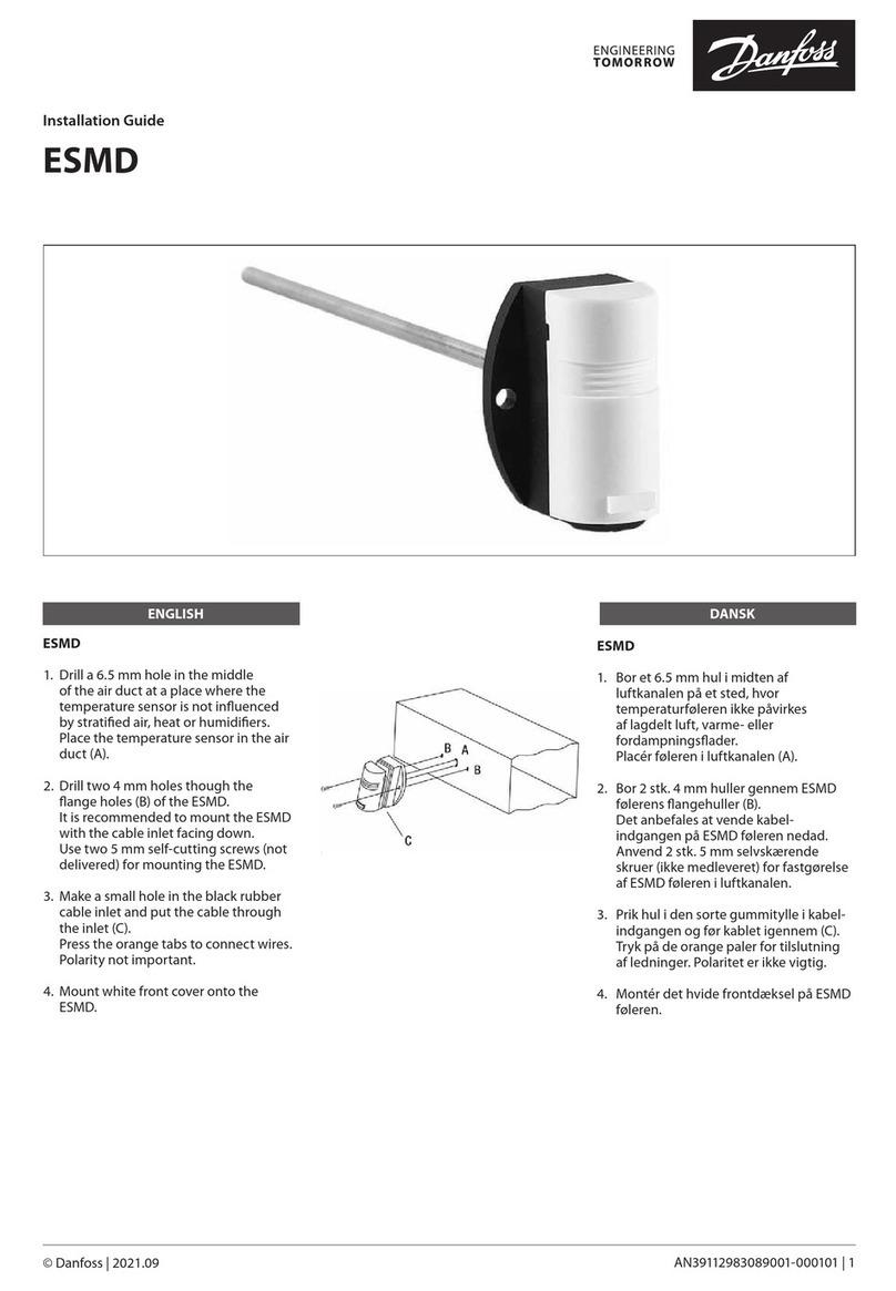
Danfoss
Danfoss ESMD installation guide

Lucent Technologies
Lucent Technologies Stinger OC3-ATM Guide


